 |
RTL to Describe the SRC, Register Transfer using Digital Logic Circuits |
| << Reverse Assembly, SRC in the form of RTL |
| Thinking Process for ISA Design >> |
Advanced Computer
Architecture-CS501
Lecture
Handouts
Computer
Architecture
Appendix
Reading
Material
Handouts
Summary
1.
Introduction
to FALSIM
2.
Preparing
source files for
FALSIM
3.
Using
FALSIM
4.
FALCON-A
assembly language
techniques
FALSIM
1.
Introduction to FALSIM:
FALSIM is
the name of the software
application which consists of
the
FALCON-A
assembler and the FALCON-A
simulator. It runs under
Windows
XP.
FALCON-A
Assembler:
Figure 1
shows a snapshot of the
FALCON-A Assembler. This
tool loads a
FALCON-A
assembly file with a (.asmfa) extension
and parses it. It
shows
the
parse results in an error
log, lets the user
view the assembled
file's
contents
in the file listing and
also provides the features
of printing the
machine
code, an Instruction Table and a
Symbol Table to a FALCON-A
listing
file. It also allows the
user to run the FALCON-A
Simulator.
The
FALCON-A Assembler has two
main modules, the 1st-pass
and the
2nd-pass.
The 1st-pass module takes an
assembly file with a
(.asmfa)
extension
and processes the file
contents. It then creates a Symbol
Table
Page
1
Last
Modified: 01-Nov-06
Advanced Computer
Architecture-CS501
which
corresponds to the storage of
all program variables, labels
and data
values in a
data structure at the implementation
level. If the
1st-pass
completes
successfully a Symbol Table is produced
as an output, which is
used by
the 2nd-pass module. Failures of the
1st-pass are handled by
the
assembler
using its exception handling
mechanism.
The
2nd-pass module sequentially processes
the .asmfa file to interpret
the
instruction
opcodes, register opcodes
and constants using the
symbol table.
It then
produces a list file with a
.lstfa extension independent of
successful
or failed
pass. If the pass is
successful a binary file
with a .binfa extension is
produced
which contains the machine code
for the program in the
assembly
file.
FALCON-A
Simulator:
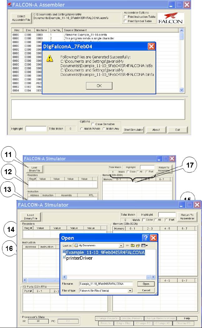
Figure 6
shows a snapshot of the
FALCON-A Simulator. This
tool loads a
FALCON-A
binary file with a (.binfa)
extension and presents its
contents
into
different areas of the
simulator. It allows the
user to execute the
program to a specific
point within a time frame or
just executes it, line
by
line. It
also allows the user to
view the registers, I/O
port values and
memory
contents
as the instructions
execute.
FALSIM
Features:
The
FALCON-A Assembler provides its
user with the following
features:
Select
Assembly File: Labeled
as "1" in
Figure 1, this feature
enables the
user to
choose a FALCON-A assembly
file and open it for
processing by the
assembler.
Assembler
Options: Labeled
as "2" in
Figure 1.
· Print
Symbol Table
This
feature if selected writes
the Symbol Table (produced
after the
execution of
the 1st-pass of the
assembler) to a FALCON-A list
file with an
extension of
(.lstfa). The Symbol Table includes
data members, data
addresses
and labels with their
respective values.
· Print
Instruction Table
This
feature if selected writes the
Instruction Table to a FALCON-A list
file
with an
extension of (.lstfa).
Page
2
Last
Modified: 01-Nov-06
Advanced Computer
Architecture-CS501
List
File: Labeled
as "3", in
Figure 1, the List File
feature gives a detailed
insight
of the FALCON-A listing
file, which is produced as a
result of the
execution of
the 1st and 2nd-pass. It
shows the Program Counter
value in
hexadecimal
and decimal formats along with
the machine code generated
for
every
line of assembly code. These
values are printed when the
2nd-pass is
completed.
Error
Log: The
Error Log is labeled as "4" in
Figure 1. It informs the
user
about the
errors and their respective
details, which occurs in any of
the
passes of
the assembler.
Search:
Search is
labeled as "5" in
Figure 1 and helps the
user to search for
a certain
input with the options of
searching with "match
whole"
and
"match
any" parts
of the string. The search
also has the option of
checking
with/without
considering "case-sensitivity". It
searches the List File
area
and
highlights the search
results using the yellow
color. It also indicates
the
total
number of matches found.
Start
Simulator: This
feature is labeled as "6" in
Figure 1. The
FALCON-A
Simulator
is run using the FALCON-A
Assembler's Start Simulator
option.
The
FALCON-A Simulator is invoked by
the user from the
FALCON-A
Assembler.
Its features are detailed as
follows:
Load
Binary File: The
button labeled as "11" in
Figure 6, allows the user
to
choose
and open a FALCON-A binary
file with a (.binfa) extension. When
a
file is
being loaded into the
simulator all the register,
constants (if any)
and
memory
values are set.
Registers:
The
area labeled as "12" in
Figure 6. enables, the user
to see
values
present in different registers
before during and after
execution.
Instruction:
This
area is labeled as "13" in
Figure 6 and contains the
value of
PC,
address of an instruction, its
representation in Assembly, the
Register
Transfer
Language, the op-code and
the instruction type.
I/O
Ports: I/O
ports are labeled as "14" in
Figure 6. These ports are
available
for
the user to enter input
operation values and visualize output
operation
values whenever an
I/O operation takes place in
the program. The
input
value
for an input operation is given by
the user before an
instruction
executes.
The output values are
visible in the I/O port
area once the
instruction
has successfully
executed.
Page
3
Last
Modified: 01-Nov-06
Advanced Computer
Architecture-CS501
Memory:
The
memory is divided into 2
areas and is labeled as "15"
in
Figure 6,
to facilitate the view of
data stored at different
memory locations
before,
during and after program
execution.
Processor's
State: Labeled
as "16" in
Figure 6, this area shows
the current
values of
the Instruction register and
the Program Counter while
the program
executes.
Search:
The
search option for the
FALCON-A simulator is labeled as
"17"
in Figure
6. This feature is similar to
the way the search
feature of the
FALCON-A
Assembler works. It offers to
highlight the search string
which
goes as
an input, with the "All "
and " Part " option. The
results of the search
are
highlighted in the color
yellow. It also indicates the
total number of
matches.
The
following is a description of the options
available on the button
panel
labeled
as "18" in
Figure 6.
Single
Step: "Single
Step" lets the user
execute the program, one
instruction
at a
time. The next instruction
is not executed unless the
user does a "single
step"
again. By default, the
instruction to be executed will be the
one next in
the
sequence. It changes if the
user specifies a different PC
value using the
Change PC
option (explained
below).
Change
PC: This
option lets the user
change the value of
PC
(Program
Counter). By changing the PC
the user can execute
the
instruction
to which the specified PC
points.
Execute:
By
choosing this button the
user is able to execute
the
instructions
with the options of execution
with/without breakpoint
insertion
(refer to Fig. 5). In case
of breakpoint insertion, the
user has
the
option to choose from a list
of valid breakpoint values. It also
has
the
option to set a limit on the
time for execution. This
"Max
Execution
Time" option restricts the program
execution to a time
frame
specified by the user, and
helps the simulator in
exception
handling.
Change
Register: Using
the Change Register feature,
the user can
change
the value present in a
particular register.
Page
4
Last
Modified: 01-Nov-06
Advanced Computer
Architecture-CS501
Change
Memory Word: This
feature enables the user to
change values
present
at a particular memory
location.
Display
Memory: Display
Memory shows an updated
memory area,
after a
particular memory location other
than the pre-existing ones
is
specified
by the user.
Change
I/O: Allows
the user to give an I/O
port value if the
instruction
to be executed requires an I/O operation.
Giving in the
input in
any one of the I/O
ports areas before
instruction execution,
indicates
that a particular I/O operation will be a
part of the program
and it
will have an input from some
source. The value given by
the
user
indicates the input type and
source.
Display
I/O: Display
I/O works in a manner similar to
Display
Memory.
Here the user specifies the
starting index of an I/O
port. This
features
displays the I/O ports
stating from the index
specified.
2.
Preparing source files for
FALSIM:
In order
to use the FALCON-A
assembler and simulator,
FALSIM,
the
source file containing
assembly language statements
and directives
should be
prepared according to the following
guidelines:
· The
source file should contain
ASCII text only. Each
line should be
terminated by a
carriage return. The extension .asmfa
should be
used
with
each file name. After
assembly, a list file with
the original
filename
and an extension .lstfa,
and a
binary file with an
extension
.binfa
will
be generated by FALSIM.
· Comments
are indicated by a semicolon (;)
and can be placed
anywhere
in the
source file. The FALSIM
assembler ignores any text
after the
semicolon.
· Names in
the source file can be of
one of the following
types:
· Variables:
These are defined using
the .equ
directive.
A value must
also be
assigned to variables when
they are defined.
· Addresses
in the "data and pointer
area" within the memory:
These
can be
defined using the .dw
or
the .sw
directive.
The difference
between
these two directives is that
when .dw
is
used, it is not
possible
to store any value in the
memory. The integer after .dw
identifies
the number of memory words to be reserved
starting at the
current
address. (The directive .db
can be
used to reserve bytes
in
Page
5
Last
Modified: 01-Nov-06
Advanced Computer
Architecture-CS501
memory.)
Using the .sw
directive,
it is possible to store a constant
or
the
value of a name in the
memory. It is also possible to
use pointers
with
this directive to specify addresses
larger than 127. Data
tables
and
jump tables can also be
set up in the memory using
this directive.
· Labels: An
assembly language statement
can have a unique
label
associated
with it. Two assembly
language statements cannot have
the
same
name. Every label should
have a colon (:) after
it.
·
Use
the .org
0 directive
as the first line in the
program. Although the
use
of this
line is optional, its use
will make sure that FALSIM
will start
simulation
by picking up the first
instruction stored at address 0 of
the
memory.
(Address 0 is called the reset
address of the processor). A
jump
[first]
instruction
can be placed at address 0, so
that control is
transferred
to the
first executable statement of
the main program. Thus, the
label
first
serves as
the identifier of the "entry
point" in the source file.
The
.org
directive
can also be used anywhere in
the source file to force
code
at a
particular address in the
memory.
·
Address 2
in the memory is reserved
for the pointer to the
Interrupt
Service
Routine (ISR). The .sw
directive
can be used to store the
address
of the
first instruction in the ISR
at this location.
Address 4
to 125 can be used for
addresses of data and
pointers1.
·
However,
the main program must start at address
126 or less2,
otherwise
FALSIM
will generate an error at the
jump
[first] instruction.
·
The
main program should be followed by any
subprograms or
procedures.
Each procedure should be terminated with
a ret
instruction.
The ISR,
if any, should be placed after
the procedures and should
be
terminated
with the iret
instruction.
·
The last
line in the source file
should be the .end
directive.
·
The
.equ
directive
can be used anywhere in the
source file to assign
values to
variables.
·
It is the
responsibility of the programmer to make
sure that code does
not
overwrite
data when the assembly
process is performed, or vice
versa. As
an example,
this can happen if care is
not exercised during the
use of the
.org
directive
in the source file.
3.
Using FALSIM:
Any
address between 4 and 14 can be used in
place of the displacement field in
load or
1
store
instructions. Recall that
the displacement field is
just 5 bits in the
instruction word.
2
This
restriction is because of the face
that the immediate operand in
the movi
instruction
must fit an 8-bit field in
the instruction word.
Page
6
Last
Modified: 01-Nov-06
Advanced Computer
Architecture-CS501
· To start
FALSIM (the FALCON-A
assembler and simulator),
double
click on
the FALSIM icon. This will
display the assembler
window,
as shown
in the Figure 1.
· Select
one or both assembler options
shown on the top right corner
of
the
assembler window labeled as
"2". If no
option is selected,
the
symbol
table and the instruction table will
not be generated in the
list
(.lstfa)
file.
· Click on
the select assembly file
button labeled as "1". This
will open
the
dialog box as shown in the
Figure 2.
· Select
the path and file containing
the source program that is to
be
assembled.
· Click on
the open button. FALSIM will
assemble the program
and
generate
two files with the
same filename, but with
different
extensions.
A list file will be generated
with an extension .lstfa, and
a
binary
(executable) file will be generated with
an extension .binfa.
FALSIM
will also display the list
file and any error
messages in two
separate
panes, as shown in Figure
3.
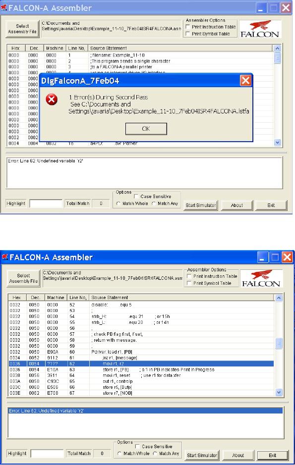
· Double
clicking on any error
message highlights and displays
the
corresponding
erroneous line in the program
listing window pane
for
the
user. This is shown in
Figure 4. The highlight
feature can also be
used to
display any text string,
including statements with
errors in
them. If
the assembler reported any
errors in the source file,
then these
errors
should be corrected and the program
should be assembled again
before
simulation can be done.
Additionally, if the source
file had
been
assembled correctly at an earlier
occasion, and a correct
binary
(.binfa)
file exists, the simulator
can be started directly
without
performing
the assembly process.
· To start
the simulator, click on the
start simulation button labeled
as
"6". This
will open the dialog box
shown in Figure 6.
· Select
the binary file to be simulated,
and click open as shown
in
Figure
7.
· This will
open the simulation window
with the executable
program
loaded in
it as shown in Figure 8. The details of
the different panes
in
Page
7
Last
Modified: 01-Nov-06
Advanced Computer
Architecture-CS501
this
window were given in section 1
earlier. Notice that the
first
instruction
at address 0 is ready for execution. All
registers are
initialized
to 0. The memory contains the
address of the ISR (i.e.,
64h
which is
100 decimal) at location 2
and the address of the
printer
driver at
location 4. These two
addresses are determined at
assembly
time in
our case. In a real
situation, these addresses will
be
determined
at execution time by the operating
system, and thus the
ISR
and the printer driver will
be located in the memory by
the
operating
system (called re-locatable code).
Subsequent memory
locations
contain constants defined in
the program.
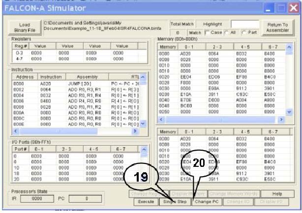
· Click
single step button labeled as
"19". FALSIM
will execute the
jump
[main] instruction
at address 0 and the PC will
change to 20h
(32
decimal), which is the
address of the first
instruction in the
main
program
(i.e., the value of
main).
· Although
in a real situation, there will be
many instructions in
the
main
program, those instructions are
not present in the dummy
calling
program.
The first useful instruction is
shown next. It loads
the
address
of the printer driver in r6
from the pointer area in
the memory.
The
registers r5 and r7 are also
set up for passing the
starting address
of the
print buffer and the number
of bytes to be printed. In
our
dummy
program, we bring these values in to
these registers from
the
data
area in the memory, and then
pass these values to the
printer
driver
using these two registers. Clicking on
the single step button
twice,
executes
these two
instructions.
· The
execution of the call instruction
simulates the event of a
print
request
by the user. This transfers
control to the printer
driver. Thus,
when
the call
r4, r6 instruction
is single stepped, the PC changes
to
32h (50
decimal) for executing the
first instruction in the
printer
driver.
· Double
click on memory location
000A, which is being used
for
holding
the PB (printer busy) flag.
Enter a 1 and click the
change
memory
button. This will store a
0001 in this location,
indicating that
a previous
print job is in progress.
Now click single step and
note that
this
value is brought from memory
location 000E into register
r1.
Clicking
single step again will cause
the jnz
r1, [message] instruction
to
execute, and control will transfer to
the message routine at
address
0046h.
The nop
instruction
is used here as a place
holder.
Page
8
Last
Modified: 01-Nov-06
Advanced Computer
Architecture-CS501
· Click
again on the single step
button. Note that when
the ret
r4
instruction
executes, the value in r4
(i.e., 28h) is brought into
the PC.
The blue
highlight bar is placed on the
next instruction after the
call
r4,
r6 instruction
in the main program. In case of
the dummy calling
program,
this is the halt
instruction.
· Double
click on the value of the PC
labeled as "20". This
will open a
dialog
box shown below. Enter
a
value
of the PC (i.e.,
26h)
corresponding
to the call
r4, r6
instruction,
so that it can
be
executed
again. A "list" of
possible
PC values
can also be pulled
down
using,
and 0026h can be
selected
from
there as well.
· Click
single step again to enter
the printer driver
again.
· Change
memory location 000A to a 0,
and then single step the
first
instruction
in the printer driver. This
will bring a 0 in r1, so that
when
the
next jnz
r1, [message] instruction
is executed, the branch will
not
be taken
and control will transfer to the
next instruction after
this
instruction.
This is mivi
r1, 1 at
address 0036h.
· Continue
single stepping.
· Notice
that a 1 has been stored in
memory location 000A, and
r1
contains 11h,
which is then transferred to the
output port at
address
3Ch (60
decimal) when the out
r1, controlp instruction
executes.
This
can be verified by double
clicking on the top left corner of
the
I/O
port pane, and changing
the address to 3Ch. Another
way to
display
the value of an I/O port is
to scroll the I/O window
pane to
the
desired position.
· Continue
single stepping till the int
instruction
and note the
changes
in
different panes of the
simulation window at each
step.
· When the
int
instruction
executes, the PC changes to 64h,
which is the
address
of the first instruction in
the ISR. Clicking single step
executes
this
instruction, and loads the
address of temp
(i.e.,
0010h) which is a
Page
9
Last
Modified: 01-Nov-06
Advanced Computer
Architecture-CS501
temporary
memory area for storing
the environment. The five
store
instructions
in the ISR save the
CPU environment (working
registers)
before
the ISR change them.
· Single
step through the ISR
while noting the effects on
various registers,
memory
locations, and I/O ports
till the iret
instruction
executes. This will
pass
control back to the printer
driver by changing the PC to
the address of
the
jump
[finish] instruction,
which is the next
instruction after the int
instruction.
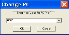
· Double
click on the value of the
PC. Change it to point to
the int
instruction
and click single step to
execute it again. Continue to single
step
till the
in
r1, statusp instruction
is ready for execution.
· Change
the I/O port at address
3Ah (which represents the
status port at
address
58) to 80 and then single step the
in
r1, statusp instruction.
The
value in
r1 should be 0080.
· Single
step twice and notice that
control is transferred to the
movi
r7,
FFFF3 instruction,
which stores an error code
of 1 in r1.
The
instruction was originally movi
r7, -1. Since it was
converted to machine
language
3
by the
assembler, and then reverse assembled by
the simulator, it became movi
r7,
FFFF.
This is
because the machine code
stores the number in 16-bits
after sign-
extension.
The result will be the same
in both cases.
Page
10
Last
Modified: 01-Nov-06
Advanced Computer
Architecture-CS501
Figure
1
Figure
2
Page
11
Last
Modified: 01-Nov-06
Advanced Computer
Architecture-CS501
Figure
3
Figure
4
Page
12
Last
Modified: 01-Nov-06
Advanced Computer
Architecture-CS501
Figure
5
Figur
e6
Page
13
Last
Modified: 01-Nov-06
Advanced Computer
Architecture-CS501
Figure
7
Figure
8
4.
FALCON-A assembly language
programming techniques:
Page
14
Last
Modified: 01-Nov-06
Advanced Computer
Architecture-CS501
· If a
signed value, x, cannot fit in 5
bits (i.e., it is outside
the range -16 to
+15),
FALSIM will report an error with a
load
r1, [x] or a store
r1, [x]
instruction.
To overcome this problem, use
movi
r2, x followed
by load
r1,
[r2].
· If a
signed value, x, cannot fit in 8
bits (i.e., it is outside
the range
-
128 to
+127), even the previous
scheme will not work. FALSIM
will
report an
error with the movi
r2, x instruction.
The following
instruction
sequence
should be used to overcome this
limitation of the
FALCON-A.
First
store the 16-bit address in
the memory using the
.sw
directive.
Then
use
two load instructions as shown
below:
a:
.sw
x
load
r2, [a]
load
r1, [r2]
This is
essentially a "memory-register-indirect" addressing.
It has been
made
possible by the .sw
directive.
The value of a
should be
less than 15.
· A similar
technique can be used with immediate ALU
instructions for
large values of
the immediate data, and with
the transfer of control
(call
and
jump) instructions for large values of
the target address.
· Large values
(16-bit values) can also be
stored in registers using
the mul
instruction
combined with the addi
instruction.
The following
instructions
bring a 201 in register
r1.
movi
r2, 10
movi
r3, 20
mul
r1, r2, r3
; r1
contains 200 after this
instruction
addi
r1, r1, 1
; r1
now contains 201
· Moving
from one register to another
can be done by using the
instruction
addi
r2, r1, 0.
· Bit
setting and clearing can be
done using the logical
(and, or, not,
etc)
instructions.
· Using
shift instructions (shiftl,
asr, etc.) is faster that mul
and
div,
if
the
multiplier
or divisor is a power of 2.
Page
15
Last
Modified: 01-Nov-06
Advanced Computer
Architecture-CS501
Lecture
Handout
Computer
Architecture
Lecture
No. 1
Reading
Material
Vincent
P. Heuring & Harry F. Jordan
Chapter
1
Computer
Systems Design and Architecture
1.1,
1.2, 1.3, 1.4,
1.5
Summary
1)
Distinction
between computer architecture,
organization and design
2)
Levels of
abstraction in digital design
3)
Introduction
to the course topics
4)
Perspectives of
different people about
computers
5)
General
operation of a stored program digital
computer
6)
The
Fetch-Execute process
7)
Concept
of an ISA(Instruction Set
Architecture)
Introduction
This
course is about Computer Architecture. We
start by explaining a few
key terms.
The
General Purpose Digital
Computer
How can
we define a `computer'? There
are several kinds of devices
that can be termed
"computers":
from desktop machines to the
microcontrollers used in appliances such
as a
microwave
oven, from the Abacus to
the cluster of tiny chips
used in parallel
processors,
etc.
For the purpose of this course, we will
use the following definition
of a computer:
"an
electronic device,
operating
under
the control of
instructions
stored
in its own memory unit,
that
can
accept data (input), process
data
arithmetically
and logically, produce
output
from the processing, and
store
the
results for future use."
[1]
Thus,
when we use the term
computer,
we
actually mean a digital
computer.
There
are many digital
computers,
which
have dedicated purposes,
for
example,
a computer used in an
automobile
that controls the
spark
Page
16
Last
Modified: 01-Nov-06

Advanced Computer
Architecture-CS501
Advanced
Computer Architecture
Lecture
No. 6
Reading
Material
Handouts
Slides
Summary
·
Using
Behavioral RTL to Describe the SRC
(continued)
·
Implementing
Register Transfer using
Digital Logic
Circuits
Using
behavioral RTL to Describe the
SRC (continued)
Once
the instruction is fetched and
the PC is incremented, execution of
the instruction
starts. In
the following discussion, we denote
instruction fetch by "iF" and
instruction
execution
by "iE".
iE:=
(
(op<4..0>=
1) : R [ra] ← M
[disp],
(op<4..0>=
2) : R [ra] ← M
[rel],
...
...
(op<4..0>=31)
: Run ← 0,);
iF);
As shown
above, instruction execution can be
described by using a long
list of
conditional
operations, which are
inherently "disjoint". Only one of
these statements is
executed,
depending on the condition
met, and then the
instruction fetch statement
(iF) is
invoked
again at the end of the list of
concurrent statements. Thus, instruction
fetch (iF)
and
instruction execution statements invoke
each other in a loop. This
is the fetch-execute
cycle of
the SRC.
Concurrent
Statements
The
long list of concurrent,
disjoint instructions of the
instruction execution (iE)
is
basically
the complete instruction set
of the processor. A brief overview of
these
instructions
is given below:
Load-Store
Instructions
(op<4..0>=
1) : R [ra] ← M
[disp], load register
(ld)
This
instruction is to load a register
using a displacement address
specified by the
instruction,
i.e., the contents of the
memory at the address `disp'
are placed in the
register
R
[ra].
(op<4..0>=
2) : R [ra] ← M
[rel], load register relative
(ldr)
Page
72
Last
Modified: 01-Nov-06
Advanced Computer
Architecture-CS501
If the
operation field `op' of the
instruction decoded is 2, the
instruction that is
executed
is
loading a register (target
address of this register is
specified by the field ra)
with
memory
contents at a relative address,
`rel'. The relative address
calculation has been
explained
in this section
earlier.
(op<4..0>=
3) : M [disp] ← R
[ra], store register
(st)
If the
op-code is 3, the contents of the
register specified by address
ra, are stored back to
the
memory, at a displacement location
`disp'.
(op<4..0>=
4) : M[rel] ← R[ra],
store register relative
(str)
If the
op-code is 4, the contents of the
register specified by the
target register address
ra,
are
stored back to the memory, at a relative
address location
`rel'.
(op<4..0>=
5) : R [ra] ← disp,
load displacement
address (la)
For
op-code 5, the displacement address disp
is loaded to the register R (specified by
the
target
register address ra).
(op<4..0>=
6) : R [ra] ← rel,
load
relative address
(lar)
For
op-code 6, the relative address
rel is loaded to the register R
(specified by the
target
register
address ra).
Branch
Instructions
(op<4..0>=
8) : (cond : PC ← R
[rb]), conditional branch
(br)
If the
op-code is 8, a conditional branch is
taken, that is, the
program counter is set to
the
target
instruction address specified by
rb, if the condition `cond'
is true.
(op<4..0>=
9) : (R [ra] ← PC,
cond
: (PC ← R
[rb]) ), branch and link
(brl)
If the op
field is 9, branch and link
instruction is executed, i.e.
the contents of the
program
counter are stored in a register
specified by ra field, (so control can be
returned
to it
later), and then the
conditional branch is taken to a
branch target address
specified by
rb.
The branch and link
instruction is useful for
returning control to the
calling program
after a
procedure call
returns.
The
conditions that these
`conditional' branches depend on,
are specified by the field
c3
that
has 3 bits. This simply
means that when
c3<2..0> is equal to one of these
six values,
we
substitute the expression on
the right hand side of
the : in place of cond.
These
conditions are explained here
briefly.
cond
:= (
c3<2..0>=0
: 0,
never
If the c3
field is 0, the branch is
never taken.
c3<2..0>=1
: 1,
always
If the
field is 1, branch is
taken
c3<2..0>=2
: R [rc]=0,
if
register is zero
If c3 = 2, a
branch is taken if the
register rc = 0.
c3<2..0>=3
: R [rc] ≠ 0,
if
register is nonzero
If c3 = 3, a
branch is taken if the
register rc is not equal to
0.
c3<2..0>=4
: R [rc]<31>=0 if positive or
zero
If c3 is 4, a
branch is taken if the
register value in the
register specified
by rc is greater
than or equal to 0.
c3<2..0>=5
: R [rc]<31>=1), if
negative
If c3 = 5, a
branch is taken if the value
stored in the register specified
by
rc is
negative.
Page
73
Last
Modified: 01-Nov-06
Advanced Computer
Architecture-CS501
Arithmetic
and Logical instructions
(op<4..0>=12)
: R [ra] ← R
[rb] + R [rc],
If the
op-code is 12, the contents of
the registers rb and rc are added and
the result is
stored in
the register ra.
(op<4..0>=13)
: R [ra] ← R
[rb] + c2<16..0> {sign
extended},
If the
op-code is 13, the content of
the register rb is added
with the immediate data in
the
field
c2, and the result is stored in
the register ra.
(op<4..0>=14)
: R [ra] ← R
[rb] R [rc],
If the
op-code is 14, the content of
the register rc is subtracted from
that of rb, and the
result is
stored in ra.
(op<4..0>=15)
: R [ra] ← -R
[rc],
If the
op-code is 15, the content of
the register rc is negated, and the
result is stored in ra.
(op<4..0>=20)
: R [ra] ← R
[rb] & R [rc],
If the op
field equals 20, logical AND of
the contents of the registers rb and rc
is obtained
and the
result is stored in register
ra.
(op<4..0>=21)
: R [ra] ← R
[rb] & c2<16..0> {sign
extended},
If the op
field equals 21, logical AND of
the content of the registers rb and
the immediate
data in
the field c2 is obtained and
the result is stored in register
ra.
(op<4..0>=22)
: R [ra] ← R
[rb] ~ R [rc],
If the op
field equals 22, logical OR of
the contents of the registers rb and rc
is obtained
and the
result is stored in register
ra.
(op<4..0>=23)
: R [ra] ← R
[rb] ~ c2<16..0> {sign
extended},
If the op
field equals 23, logical OR of
the content of the registers rb and
the immediate
data in
the field c2 is obtained and
the result is stored in register
ra.
(op<4..0>=24)
: R [ra] ← !R
[rc],
If the
op-code equals 24, the content of
the logical NOT of the
register rc is obtained, and
the
result is stored in ra.
Shift
instructions
(op<4..0>=26):
R [ra]<31..0 > ← (n α 0) R
[rb] <31..n>,
If the
op-code is 26, the contents of
the register rb are shifted
right n bits times. The
bits
that
are shifted out of the
register are discarded. 0s are
added in their place, i.e. n
number
of 0s is
added (or concatenated) with
the register contents. The
result is copied to the
register
ra.
(op<4..0>=27)
: R [ra]<31..0 > ← (n α R
[rb] <31>) R [rb]
<31..n>,
For
op-code 27, shift arithmetic
operation is carried out. In
this operation, the contents
of
the
register rb are shifted
right n times, with the
most significant bit, i.e.,
bit 31, of the
register
rb added in their place. The
result is copied to the register
ra.
(op<4..0>=28)
: R [ra]<31..0 > ← R
[rb] <31-n..0> (n α 0),
For
op-code 28, the contents of
the register rb are shifted
left n bits times, similar
to the
shift
right instruction. The
result is copied to the register
ra.
(op<4..0>=29)
: R [ra]<31..0 > ← R
[rb] <31-n..0> R [rb]<31..32-n
>,
The
instruction corresponding to op-code 29 is
the shift circular
instruction. The
contents
of the
register rb are shifted left
n times, however, the bits
that move out of the
register in
the
shift process are not
discarded; instead, these are shifted in
from the other end (a
circular
shifting). The result is stored in
register ra.
where
n := (
(c3<4..0>=0) : R [rc],
Page
74
Last
Modified: 01-Nov-06
Advanced Computer
Architecture-CS501
(c3<4..0>!=0)
: c3 <4..0> ),
Notation:
α means
replication
means concatenation
Miscellaneous
instructions
(op<4..0>=
0) ,
No
operation (nop)
If the
op-code is 0, no operation is carried out
for that clock period.
This instruction is
used as a
stall in pipelining.
(op<4..0>=
31) : Run ← 0,
Halt the processor
(Stop)
); iF
);
If the
op-code is 31, run is set to 0,
that is, the processor
stops execution.
After one
of these disjoint instructions is
executed, iF, i.e.
instruction Fetch is carried
out
once
again, and so the fetch-execute
cycle continues.
Implementing
Register Transfers using
Digital Logic
Circuits
We have
studied the register
transfers in the previous sections, and
how they help in
implementing
assembly language. In this
section we will review how
the basic digital
logic
circuits are used to
implement instructions register
transfers. The topics we
will
cover in
this section include:
1. A
brief (and necessary) review of
logic circuits
2.
Implementing simple register
transfers
3.
Register file implementation
using a bus
4.
Implementing register transfers
with mathematical
operations
5. The
Barrel Shifter
6.
Implementing shift
operations
Review of
logic circuits
Before we
study the implementation of
register transfers using
logic circuits, a
brief
overview
of some of the important
logic circuits will prove
helpful. The topics we
review
in this
section include
1. The
basic D flip flop
2. The
n-bit register
3. The
n-to-1 multiplexer
4.
Tri-state buffers
The
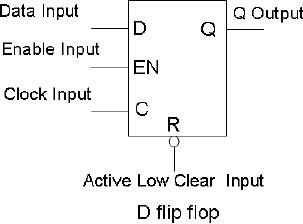
basic D flip flop
A
flip-flop is a bi-stable
device,
capable
of storing one bit of
Information.
Therefore, flip-flops
are
used as the building blocks
of a
computer's
memory as well as CPU
registers.
Page
75
Last
Modified: 01-Nov-06
Advanced Computer
Architecture-CS501
There
are various types of
flip-flops; most common
type, the D flip-flop is
shown in the
figure
given. The given truth
table for this positive-edge
triggered D flip-flop shows
that
the
flip-flop is set (i.e.
stores a 1) when the data
input is high on the leading
(also called
the
positive) edge of the clock;
it is reset (i.e., the
flip-flop stores a 0) when
the data input
is 0 on
the leading edge of the
clock. The clear input will
reset the flip-flop on a
low
input.
The
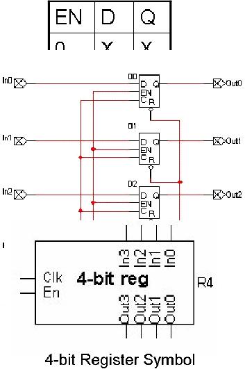
n-bit register
A n-bit
register can be formed by
grouping
n flip-flops together. So a
register
is a device in which a
group of
flip-flops operate
synchronously.
A
register is useful for
storing
binary
data, as each flip-flop
can
store one
bit. The clock input
of
the
flip-flops is
grouped
together,
as is the enable input.
As shown
in the figure, using
the
input lines a binary
number
can be stored in
the register by
applying
the corresponding
logic
level to each of the
flip-
flops
simultaneously at
the
positive
edge of the clock.
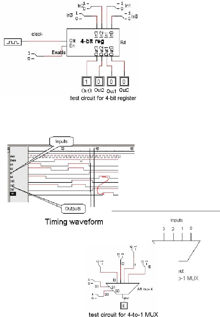
The
next figure shows
the
symbol of
a 4-bit register used
for an
integrated circuit.
In0
through
In3 are the four
input
lines,
Out0 through Out3 are
the
four
output lines, Clk is
the
clock
input, and En is the enable
line.
To
get
a
better
understanding
of this register,
consider
the situation where we
want
to store
the binary number 1000 in
the
register.
We will apply the number
to
the
input lines, as shown in the
figure given.
On the
leading edge of the clock,
the number will be stored in the
register. The enable
input
has to be high if the number
is to be stored into the
register.
.
Page
76
Last
Modified: 01-Nov-06
Advanced Computer
Architecture-CS501
Waveform/Timing
diagram
The
n-to-1 multiplexer
A
multiplexer is a device,
constructed
through
combinational logic,
which
takes n
inputs and transfers one of
them as
the output at a time. The
input
that is
selected as the output
depends
on the
selection lines, also called
the
control
input lines. For an
n-to-1
Page
77
Last
Modified: 01-Nov-06
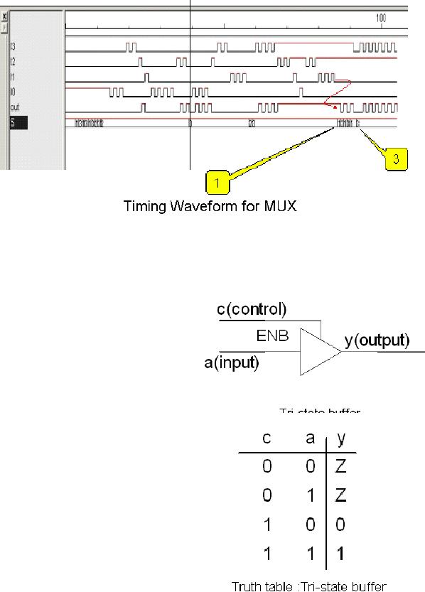
Advanced Computer
Architecture-CS501
multiplexer,
there are n input lines,
log2n control lines,
and 1 output line. The
given
figure
shows a 4-to-1 multiplexer.
There are 4 input lines; we
number these lines as line
0
through
line 3. Subsequently, there
are 2 select lines (as
log24 = 2).
For a
better understanding, let us
consider a case where we
want to transfer the input
of
line 3 to
the output of the
multiplexer. We will need to apply
the binary number 11 on
the
select
lines (as the binary
number 11 represents the
decimal number 3). By doing
so, the
output of
the multiplexer will be the
input on line 3, as shown in
the test circuit
given.
Timing
waveform
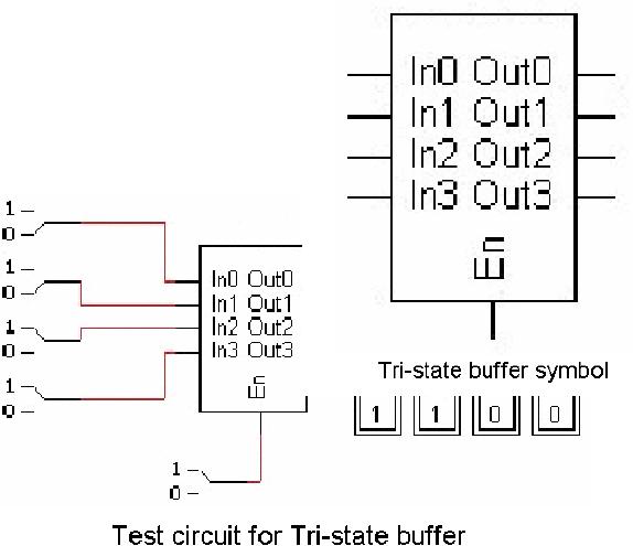
Tri-state
buffers
The
tri-state buffer, also called
the three-
state
buffer, is another
important
component
in the digital logic domain.
It
has a
single input, a single
output, and
an enable
line. The input is
concatenated
to the
output only if it is enabled
through
the
enable line, otherwise it gives a
high
impedance
output, i.e. it is tri-stated,
or
electrically
disconnected from the
input
These
buffers are available both
in the
inverting
and the non-inverting form.
The
inverting
tri-state buffers output
the
`inverted'
input when they are
enabled,
as
opposed to their
non-inverting
counterparts
that simply output the
input
when
enabled. The circuit symbol of
the
tri-state
buffers is shown. The truth
table
Page
78
Last
Modified: 01-Nov-06
Advanced Computer
Architecture-CS501
further
clarifies the working of a
non-inverting tri-state
buffer.
We can
see that when the enable
input (or the control
input) c is low (0), the
output is
high
impedance Z. The symbol of a 4-bit
tri-state buffer unit is
shown in the figure.
There
are
four input lines, an equal
number of
output
lines, and an enable line in
this
unit. If
we apply a high on the input
3
and 2, and a
low on input 1 and 0, we
get the
output 1100, only when
the
enable
input is high, as shown in
the
given
figure.
Implementing
simple register
transfers
We now
build on our knowledge of
the primitive logic circuits
to understand how
register
transfers
are implemented. In this
section we will study the
implementation of the
following
· Simple
conditional transfer
· Concept
of control signals
· Two-way
transfers
· Connecting
multiple registers
· Buses
· Bus
implementations
Simple
conditional transfer
In a
simple conditional transfer, a
condition is checked, and if it is true,
the register
transfer
takes place. Formally, a
conditional transfer is represented
as
Cond: RD
←
RS
This
means that if the condition
`Cond' is true, the contents
of the register named RS
(the
source
register) are copied to the
register RD (the destination
register). The
following
figure
shows how the registers may
be interconnected to achieve a
conditional transfer. In
Page
79
Last
Modified: 01-Nov-06
Advanced Computer
Architecture-CS501
this
circuit, the output of the
source register RS is connected to the
input of the
destination
registers RD. However, notice
that the transfer will not
take place unless the
enable
input of the destination
register is activated. We may say
that the `transfer'
is
being
controlled by the enable line
(or the control signal).
Now, we are able to control
the
transfer
by selectively enabling the
control signal, through the
use of other
combinational
logic
that may be the equivalent
of our condition. The
condition is, in general, a
Boolean
expression,
and in this example, the
condition is equivalent to LRD
=1.
Two-way
transfers
In the
above example, only one-way
transfer was possible, i.e., we could
only copy the
contents
of RS to RD if the condition was met. In
order to be able to achieve
two-way
transfers,
we must also provide a path
from the output of the
register RD to input of
register
RS. This will enable us to
implement
Cond1: RD
←
RS
Cond2: RS
←
RD
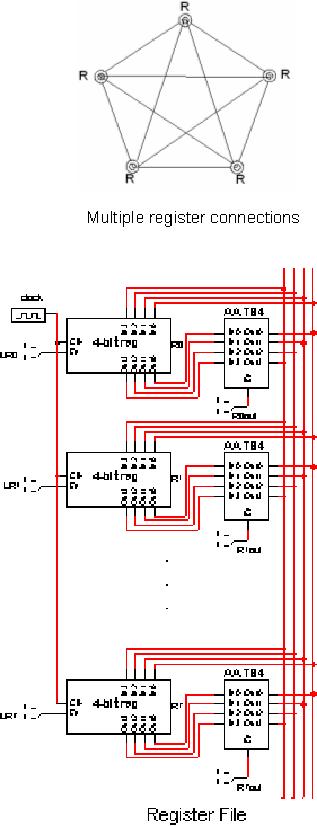
Connecting
multiple registers
We have
seen how two registers can be
connected. However, in a computer we
need to
connect
more than just two
registers. In order to connect these
registers, one may argue
that a
connection between the input
and output of each be provided.
This solution is
shown
for a scenario where there
are 5 registers that need to be
interconnected.
We can
see that in this solution,
an m-bit register requires
two connections of
m-wires
each.
Hence five m-bit registers in a
"point-to-point" scheme require 20
connections;
each
with m wires. In general, n registers in
a point to point scheme
require n (n-1)
connections.
It is quite obvious that
this solution is not going
to scale well for a
large
Page
80
Last
Modified: 01-Nov-06
Advanced Computer
Architecture-CS501
number of
registers, as is the case in real
machines. The solution to
this problem is the
use of a
bus architecture, which is explained in
the following sections.
Buses
A bus is a
device that provides a
shared data
path to a
number of devices that are
connected
to it,
via a `set of wires' or a `set of
conductors'.
The modern computer
systems
extensively
employ the bus
architecture.
Control
signals are needed to decide
which two
entities
communicate using the shared
medium,
i.e.
the bus, at any given
time. This control
signals
can be open collector
gate
based, tri-state
buffer
based,
or they can be
implemented
using
multiplexers.
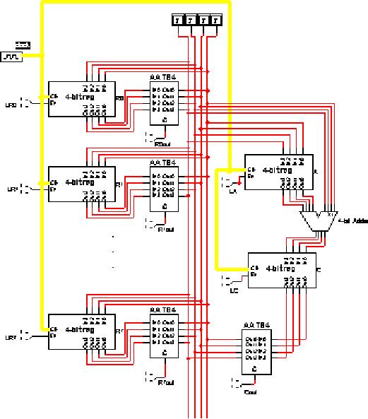
Register
file implementation
using
the bus architecture
A number
of registers can be
inter-connected
to form a
register
file, through the use of
a
bus.
The given diagram
shows
eight
4-bit registers (R0, R1,
...,
R7)
interconnected through a 4-
bit bus
using 4-bit tri-state
buffer
units (labeled
AA_TS4).
The
contents of a particular
register
can be transferred onto
the bus
by applying a logical
high
input on the enable of
the
corresponding
tri-state buffer.
For
instance, R1out can be
used
to enable
the tri-state buffers
of
the
register R1, and in
turn
transfer
the contents of the
register
on the bus.
Once
the contents of a
particular
register
are on the bus,
the
contents
may be transferred, or
read
into any other
register.
More
than one register may
be
written
in this manner;
however,
only one
register can write
its
value on
the bus at a given
time.
Page
81
Last
Modified: 01-Nov-06
Advanced Computer
Architecture-CS501
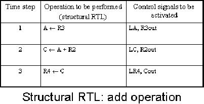
Implementing
register transfers with
mathematical operations
We have
studied the implementation of
simple register transfers;
however, we frequently
encounter
register transfers with
mathematical operations. An example
is
(opc=1):
R4←
R3 +
R2;
These
mathematical operations may be
achieved by introducing
appropriate
combinational
logic; the above operation can be
implemented in hardware by including
a
4-bit
adder with the register
files connected through the
bus. There are two
more registers
in this
configuration, one for holding one of
the operands, and the other
for holding the
result
before it is transferred to the
destination register. This is
shown in the figure
below.
Page
82
Last
Modified: 01-Nov-06
Advanced Computer
Architecture-CS501
We now
take a look at
the
steps taken for
the
(conditional,
mathematical)
transfer
(opc=1):
R4←
R3 +
R2.
First
of all, if
the
condition
opc = 1 is met,
the
contents of the first
operand
register, R3, are
transferred
to
the
temporary
register A
through
the bus. This is
done
by
activating
R3out. It
lets the contents of the
register R3 to be loaded on the bus. At
the same time,
applying
a logical high input to LA
enables the load for
the register A. This lets
the
binary
number on the bus (the
contents of register R3) to be loaded
into the register A.
The
next step is to enable R2out to
load the contents of the
register R2 onto the bus.
As
can be observed
from the figure, the
output of the register A is one of
the inputs to the 4-
bit
adder; the other input to
the adder is the bus itself.
Therefore, as the contents
of
register
R2 are loaded onto the bus,
both the operands are
available to the adder.
The
output
can then be stored to the register RC by
enabling its write. So a
high input is
applied
to LC to store the result in register
RC.
The
third and final step is to store
(transfer) the resultant
number in the
destination
register
R4. This is done by enabling
Cout, which writes the
number onto the bus,
and
then
enabling the read of the
register R4 by activating the
control signal to LR4.
These
steps
are summarized in the given
table.
The
barrel shifter
Shift
operations are frequently
used operations, as shifts can be
used for the
implementation
of multiplication and division etc. A
bi-directional shift register
with a
parallel
load capability can be used to
perform shift operations.
However, the delays
in
such
structures are dependent on the
number of shifts that are to
be performed, e.g., a 9
bit
shift requires nine clock
periods, as one shift is performed per
clock cycle. This is
not
an
optimal solution. The barrel
shifter is an alternative, with
any number of shifts
accomplished
during a single clock
period. Barrel shifters are
constructed by using
multiplexers.
An n-bit barrel shifter is a
combinational circuit implemented
using n
multiplexers.
The barrel provides a
shifted copy of the input
data at its output.
Control
inputs
are provided to specify the
number of times the input
data is to be shifted.
The
shift
process can be a simple one with 0s
used as fillers, or it can be a rotation
of the input
data.
The corresponding figure
shows a barrel shifter that
shifts right the input data;
the
number of
shifts depends on the bit
pattern applied on the
control inputs S0,
S1.
The
function table for the
barrel shifter is given. We
see from the table
that in order to
apply
single shift to the input
number, the control signal
is 01 on (S1, S0), which is
the
binary
equivalent of the decimal
number 1. Similarly, to apply 2
shifts, control signal
10
Page
83
Last
Modified: 01-Nov-06
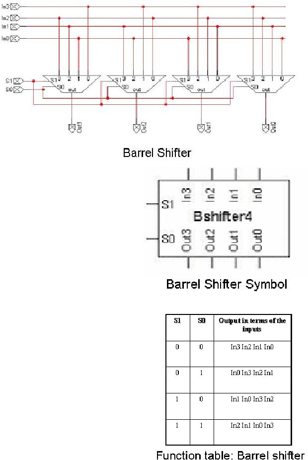
Advanced Computer
Architecture-CS501
(on
S1, S0) is applied; 10 is the
binary
equivalent
of the decimal number 2.
A
control
input of 11 shifts the
number 3
places to
the right.
Now we
take a look at an example of
the
shift operation being
implemented
through
the use of the barrel
shifter:
R4← ror R3 (2
times);
The
shift functionality can
be
incorporated
into the register
file
circuit
with the bus architecture
we
have
been building, by introducing
the
barrel
shifter, as shown in the
given
figure.
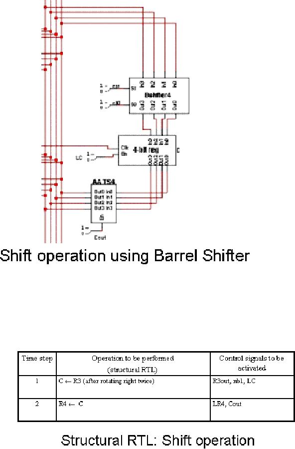
To
perform the
operation,
R4← ror R3 (2
times),
the
first step is to activate
R3out, nb1
and LC.
Activating R3out will load
the
contents
of the register R3 onto the
bus.
Since the
bus is directly connected to
the
input of the barrel shifter,
this
number is
applied to the input side.
nb1
and nb0
are the barrel shifter's
control
lines
for specifying the number of
shifts
to be
applied. Applying a high
input to
nb1 and a
low input to nb0 will shift
the
number
two places to the
right.
Activating
LC will load the
shifted
output of
the barrel shifter into
the
Page
84
Last
Modified: 01-Nov-06
Advanced Computer
Architecture-CS501
register
C. The second step is to
transfer the contents of the
register C to the register
R4.
This is
done by activating the control
Cout, which will load the
contents of register C
onto
the data bus, and by
activating the control LR4,
which will let the contents
of the
bus be
written to the register R4.
This will complete the
conditional shift-and-store
operation.
These steps are summarized in
the table shown
below.
Page
85
Last
Modified: 01-Nov-06
Table of Contents:
- Computer Architecture, Organization and Design
- Foundations of Computer Architecture, RISC and CISC
- Measures of Performance SRC Features and Instruction Formats
- ISA, Instruction Formats, Coding and Hand Assembly
- Reverse Assembly, SRC in the form of RTL
- RTL to Describe the SRC, Register Transfer using Digital Logic Circuits
- Thinking Process for ISA Design
- Introduction to the ISA of the FALCON-A and Examples
- Behavioral Register Transfer Language for FALCON-A, The EAGLE
- The FALCON-E, Instruction Set Architecture Comparison
- CISC microprocessor:The Motorola MC68000, RISC Architecture:The SPARC
- Design Process, Uni-Bus implementation for the SRC, Structural RTL for the SRC instructions
- Structural RTL Description of the SRC and FALCON-A
- External FALCON-A CPU Interface
- Logic Design for the Uni-bus SRC, Control Signals Generation in SRC
- Control Unit, 2-Bus Implementation of the SRC Data Path
- 3-bus implementation for the SRC, Machine Exceptions, Reset
- SRC Exception Processing Mechanism, Pipelining, Pipeline Design
- Adapting SRC instructions for Pipelined, Control Signals
- SRC, RTL, Data Dependence Distance, Forwarding, Compiler Solution to Hazards
- Data Forwarding Hardware, Superscalar, VLIW Architecture
- Microprogramming, General Microcoded Controller, Horizontal and Vertical Schemes
- I/O Subsystems, Components, Memory Mapped vs Isolated, Serial and Parallel Transfers
- Designing Parallel Input Output Ports, SAD, NUXI, Address Decoder , Delay Interval
- Designing a Parallel Input Port, Memory Mapped Input Output Ports, wrap around, Data Bus Multiplexing
- Programmed Input Output for FALCON-A and SRC
- Programmed Input Output Driver for SRC, Input Output
- Comparison of Interrupt driven Input Output and Polling
- Preparing source files for FALSIM, FALCON-A assembly language techniques
- Nested Interrupts, Interrupt Mask, DMA
- Direct Memory Access - DMA
- Semiconductor Memory vs Hard Disk, Mechanical Delays and Flash Memory
- Hard Drive Technologies
- Arithmetic Logic Shift Unit - ALSU, Radix Conversion, Fixed Point Numbers
- Overflow, Implementations of the adder, Unsigned and Signed Multiplication
- NxN Crossbar Design for Barrel Rotator, IEEE Floating-Point, Addition, Subtraction, Multiplication, Division
- CPU to Memory Interface, Static RAM, One two Dimensional Memory Cells, Matrix and Tree Decoders
- Memory Modules, Read Only Memory, ROM, Cache
- Cache Organization and Functions, Cache Controller Logic, Cache Strategies
- Virtual Memory Organization
- DRAM, Pipelining, Pre-charging and Parallelism, Hit Rate and Miss Rate, Access Time, Cache
- Performance of I/O Subsystems, Server Utilization, Asynchronous I/O and operating system
- Difference between distributed computing and computer networks
- Physical Media, Shared Medium, Switched Medium, Network Topologies, Seven-layer OSI Model