 |
External FALCON-A CPU Interface |
| << Structural RTL Description of the SRC and FALCON-A |
| Logic Design for the Uni-bus SRC, Control Signals Generation in SRC >> |

Advanced Computer
Architecture-CS501
Advanced
Computer Architecture
Lecture
No. 14
Reading
Material
Handouts
Slides
Summary
·
Structural
RTL Description of the FALCON-A
(continued...)
·
External
FALCON-A CPU
Interface
This
lecture is a continuation of the
previous lecture.
Un-conditional
jump instruction
jump
(op-code= 20)
In the
un-conditional jump with op-code
20, the op-code is followed by a
3-bit identifier
for
register ra and then followed by an
8-bit constant c2.
Forms
allowed by the assembler to
define the jump are as
follows:
jump
[ra + constant]
jump
[ra + variable]
jump
[ra + address]
jump
[ra + label]
For
all the above
instructions:
(ra=0):PC← PC+(8αC2<7>)©C2<7..0>,
(ra≠0):PC← R[ra]+(8αC2<7>)©C2<7..0>;4
In the
case of a constant, variable, an address
or (label-PC) the jump
ranges from 128 to 127
because of the restriction on
8-bit
constant
c2. Now, for example if we have
jump [r0+a], it means jump
to a. On the other hand if we have
jump [ r2] that is
not
allowed by
the assembler. The target
address should be even because we
have each instruction with 2
bytes. So the types
available for
the
un-conditional jumps are either direct,
indirect, PC-relative or register
relative. In the case of direct
jump the constant c2
would
define
the target address and in
the case of indirect jump
constant c2 would define the indirect
location of memory from
where we
could
find out the address to
jump. While in the case of
PC-relative if the contents of
register ra are zero then we
have near jump
and
the
type of jump for this would be
PC-relative. If ra is not be zero then we
have a far jump and
the contents of register ra
will be added
with
the constant c2 after sign-extension to
determine the jump
address.
4
c2 is
computed by sign extending
the constant,variable,address or
(label-PC)
Page
165
Last
Modified: 01-Nov-06
Advanced Computer
Architecture-CS501
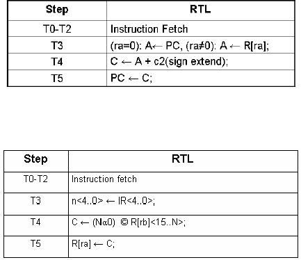
Structural
RTL description for
un-conditional jump
instruction
jump
[ra+c2]
In first
three steps, T0-T2, we would
fetch the jump instruction,
while in T3 we would either take the
contents of PC and place
them in
a temporary
register A if the condition
given in jump instruction is true, that
is if the ra field is zero,
otherwise we would place
the
contents
of register ra in the temporary register
A. Comma `,' indicates that these
two instructions are concurrent
and only one of
them
would
execute at a time. If the ra
field is zero then it would be
PC-relative jump otherwise it would be
register-relative jump. In step
T4 we would
add the constant c2 after
sign-extension to the contents of temporary
register A. As a result we would have the
effective
address
in the buffer register C, to
which
we need
to jump. In step T5 we will
take
the
contents of C and load it in
the PC,
which
would be the required address for
the
jump.
Structural
RTL
for
the
shift
instruction
shiftr
ra, rb, c1
First
three steps would fetch the
shift
instruction.
c1 is the count field. It is a 5-
bit
constant and is obtained from
the lower 5-bits of the
instruction register IR. In
step T3 we would load the
5-bit register `n' from
the
count
field or the lower 5-bits of
the IR and then in T4 depending upon
the value of `N' which indicates
the decimal value of `n',
we
would take
the contents of register rb
and shift right by N-bits
which would indicate how
many shifts are to be performed.
`n'
indicates
the register while `N'
indicates the decimal value of the
bits present in the register
`n'. So as a result we need to copy
the
zeros to
the left most bits, this
shows that zeros are replicated
`N' times and are
concatenated with the shifted
bits that are
actually
15...N.
In T5, we take the contents
from
C through
the bus and feed it to
the
register
ra which is the destination
register.
Other instructions that would
have
similar tables are `shiftl'
and `asr'.
In case
of asr, when the data is
shifted
right,
instead of copying zeros on the
left
side, we
would copy the sign bit from
the
original
data to the left-most
position.
Other
instructions
Other instructions
are mov, call and
ret.
Note that
these instructions were not
available with the SRC
processor.
Page
166
Last
Modified: 01-Nov-06
Advanced Computer
Architecture-CS501
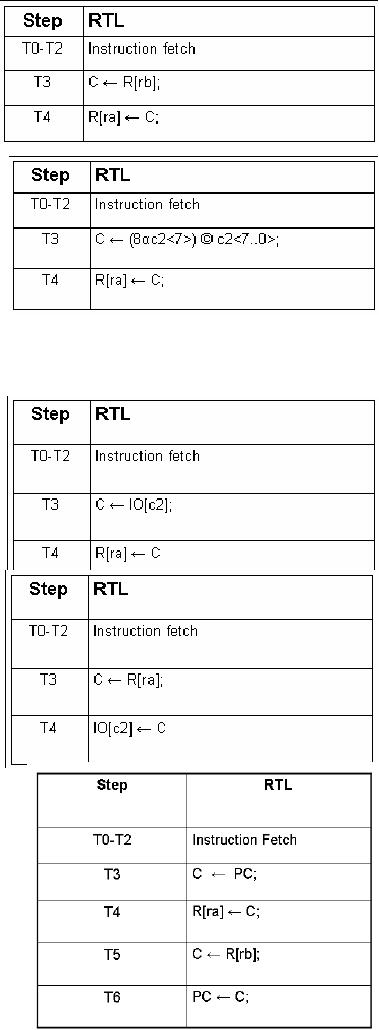
Structural
RTL for the mov
instruction
mov
ra, rb
In mov
instruction the data in
register rb, which is
the
source register, is to be moved in
the register ra,
which is
the destination register. In first three
steps,
mov
instruction is fetched. In step T3
the contents of
register
rb are placed in buffer
register C through the
ALSU
unit while in step T4 the
buffer register C
transfers
the data to register ra through
internal uni-
bus.
Structural
RTL
for
the
mov
immediate
instruction
movi
ra, c2
In this
instruction ra is the destination
register and
constant
c2 is to be moved in the ra.
First three steps
would
fetch the move immediate
instruction. In step
T3 we would take
the constant c2 and place it
into the
buffer
register C. Buffer register C is 16-bit
register
and c2 is
8-bit constant so we need to
concatenate the
remaining
leftmost bits with the sign
bit which is bit
`7'
shown within angle brackets.
This sign bit which
is
the most
significant bit would be `1' if
the number is
negative
and `0' if the number is
positive. So
depending upon
this sign bit the remaining
8-bits are replicated with this sign
bit to make a 16-bit
constant to be placed in the
buffer
register
C. In step T4 the contents of C
are taken to the destination register
ra.
In case
of FALCON-A, `in' and `out'
instructions are present which
are not present in the
SRC processor. So, for this
we assume that
there
would be interconnection with the input
and output addresses up to
0..255.
Structural
RTL for the in
instruction
in
ra, c2
First
three steps would fetch the
instruction In step T3
we take
the IO [c2] which indicates that go to
IO
address
indicated by c2 which is a positive
constant in
this
case and then data would be
taken to the buffer
register
C. In step T4 we would transfer the
data from
C to the
destination register ra.
Structural
RTL for the out
instruction
out
ra, c2
This
instruction is opposite to the `in'
instruction.
First
three instructions would fetch the
instruction. In
step T3
the contents of register ra
are placed in to the
buffer
register C and then in Step T4
from C the data
is placed
at the output port indicated
by the c2
constant.
So this instruction is just opposite to
the `in'
instruction.
Structural
RTL for the call
instruction
call
ra, rb
In this
instruction we need to give
the control to the
procedure,
sub-routine or to another address
specified
in the
program. First three steps would
fetch the call
instruction.
In step T3 we store the
present contents of
PC in to
the buffer register C and
then from C we transfer
the
data to the register ra in
step T4. As a result register
ra
would contain
the original contents of PC
and this would
be a
pointer to come back after executing
the sub-routine
and it
would be later used by a return instruction. In
step
T5 we take
the contents of register rb,
which would
actually
indicate to the point where
we want to go. So in
step T6
the contents of C are placed
in PC and as a result
PC would
indicate the position in the
memory from where
new
execution has to begin.
Page
167
Last
Modified: 01-Nov-06
Advanced Computer
Architecture-CS501
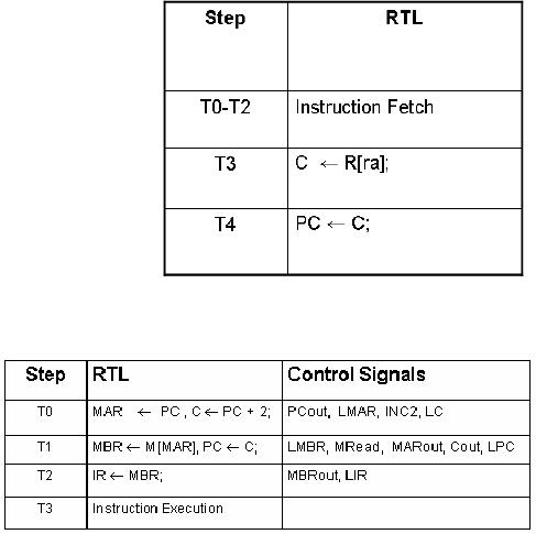
Structural
RTL
for
return
instruction
ret
ra
After
instruction fetch in first 3
steps
T0-T2,
the register data in ra is
placed
in the
buffer register C through
ALSU
unit. PC
is loaded with contents of
this
buffer
register in step T4.
Assuming
that bus
activity is synchronized,
appropriate
control signals
are
available
to us now.
Control
signals required at
different
timing
steps
of
FALCON-A
instructions
The
following table shows the
details of the control
signals needed. The first
column is
the
time step, as before. In the
second column the structural
RTLs for the particular
step
is given,
and the
corresponding
control
signals are
shown in
the third
column.
Internal bus
is active
in step T0,
causing
the contents
of the PC
to be
placed in
the Memory Address register MAR and
simultaneously the PC is
incremented
by 2 and placed it in
the buffer register C.
Recalling previous lectures, to
write data in to
a
particular register we need to enable
the load signal. In case of
fetch instruction in
step
T0,
control signal LMAR is enabled to cause
the data from internal bus
to be written in to
the
address register. To provide
data to the bus through
tri-state buffers we need
to
activate
the `out' control signal
named as `PCout', making contents of
the PC available to
the
ALSU and so control unit
provides the increment
signal `INC2' to increment
the PC.
As the
ALSU is the combinational
circuit, the PCout signal
causes the contents over
the
2nd
input of ALSU incremented by 2 and so
the data is available in
buffer register C.
Control
signal "LC" is required to
write data into the
buffer register C form the
ALSU
output.
Now note that `INC2' is one
of the ALSU functions and also it is a
control signal.
So
knowing the control signals,
which need to be activated at a
particular step, is
very
important.
So, at
step T0 the control signal
`PCout' is activated to provide
data to the internal
bus.
Now
control signal `LMAR' causes
the data from the bus to be
read into the
register
MAR. The
ALSU function `INC2'
increments the PC to 2 and the
output are stored in
the
buffer
register C by the control
signal `LC'. The data
from memory location
addressed by
MAR is
read into Memory Buffer
Register MBR in the next
timing step T1. In the
mean
time
there is no activity on the
internal bus, the output
from the buffer register C
(the
incremented
value of the PC) is placed in the PC
through bus. For this
the control signal
`LPC' is
activated.
To enable
tri-state buffer of Memory Address
Register MAR, we need control
signal
`MARout'.
Another control signal is
required in step T1 to enable memory
read i.e.
`MRead'.
In order to enable buffer register C to
provide its data to the bus
we need
Page
168
Last
Modified: 01-Nov-06
Advanced Computer
Architecture-CS501
`Cout'
control signal and in order to enable
the PC to read from C we
need to enable its
load
signal, which is `LPC'. To
read data coming from
memory into the Memory
Buffer
Register
MBR, `LMBR'control signal is enabled. So
in T2 we need 5 control signals,
as
shown.
In T2,
the instruction register IR is loaded
with data from the
MBR, so we need two-
control
signals,'MBRout' to enable its tri-state
buffers and the other signal
required is the
load
signal for IR register `LIR'.
Fetch operation is completed in
steps T0-T2 and
appropriate
control signals are generated.
Those control signals, which
are not shown,
would
remain de-activated. All control
signals are activated
simultaneously so the
order
of these
controls signals is immaterial.
Recall that in SRC the fetch
operation is
implemented
in the same way, but
`INC4' is used instead of `INC2'
because the
instruction
length is 4 bytes.
Now we
take a look at other examples
for control signals required
during execution
phase.
For
various instructions, we will define
other control signals needed
in the execution
phase of
each instruction but fetch
cycle will be the same for
all instructions.
Another
important fact is the
interface of the CPU with an
external memory and the
I/O
depending
upon whether the I/O is
memory mapped or non-memory
mapped. The
processor
will generate some control
signals, used by the memory
or I/O to read/write
data
to/from the I/O devices or from
the memory. Another
assumption is that the
memory
read is
fast enough. Therefore data
from memory must be
available to the processor in
a
fixed
time interval, which in this
particular example is
T2.
For a
slow data transfer, the
concept of handshaking is used.
Some idle states
are
introduced
and buffer is prepared until
the data is available. But
for simplicity, we will
assume
that memory is fast enough
and data is available in buffer
register MBR to the
CPU.
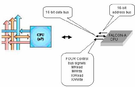
External
FALCON-A CPU
Interface
This
figure is a symbolic
representation
of the
FALCON-A
in the form of
a chip.
The external
interface
consists of a 16-
bit
address bus, a 16-bit
data bus
and a control bus
on which
different control signals
like MRead, MWrite, IORead,
IOWrite are present.
Page
169
Last
Modified: 01-Nov-06
Advanced Computer
Architecture-CS501
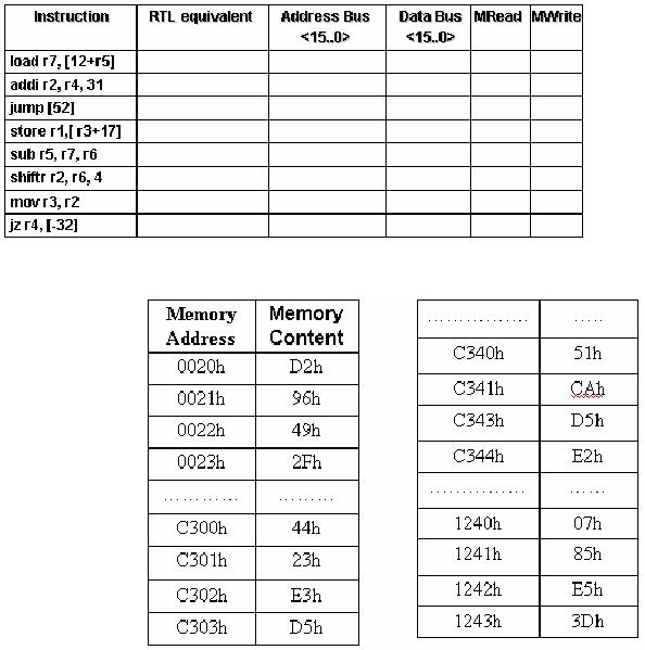
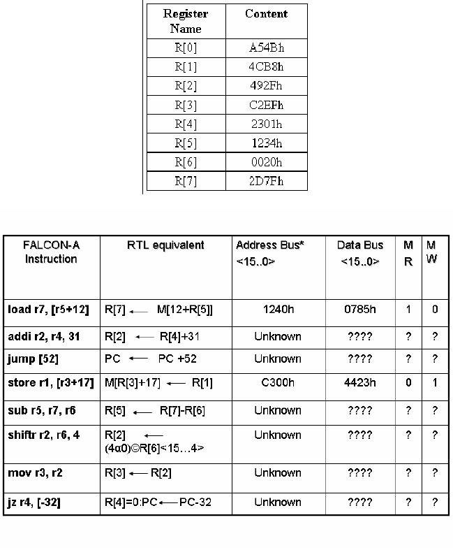
Example
Problem
(a)
What will be the logic
levels on the external
FALCON-A buses when each of
the
given
FALCON-A
instruction
is executing
on the
processor?
Complete
the table
given.
All numbers are
in the
decimal number
system,
unless noted
otherwise.
(b)
Specify memory-
addressing
modes for
each of
the FALCON-
A
instructions given.
Assumptions
For
this particular
example
we
will
assume
that all memory
contents
are properly
aligned,
i.e. memory addresses start
at address divisible by 2.
PC=
C348h
This
table contains a partial
memory map showing the
addresses and the
corresponding
data
values.
The
next table shows the
register map showing the
contents of all the CPU
registers.
Another
important thing to note is
that memory storage is
big-endian.
Page
170
Last
Modified: 01-Nov-06
Advanced Computer
Architecture-CS501
Solution:
In this
table the second column
contains the RTL descriptions of
the instructions. We
have to
specify the address bus and
data bus contents for each
instruction execution.
For
load
instruction the contents of
register r5+12 are placed on
the address bus.
From
register
map shown in the previous
table we can see that the
contents of r5 are
1234h.
Now
contents of r5 are added
with displacement value 12 in
decimal .In other words
the
address
bus will carry the hexadecimal
value 1234h+ Ch = 1240h.Now
for load
instruction,
the contents of memory
location at address 1240h will be placed
on the data
bus.
From the memory map shown in
the previous table we can
see that memory
location
1240h
contains 785h. Now to read
this data from this
location, MRead control
signal will
be
activated shown by 1 in the
next column and MWrite would
be 0.Similarly RTL
Page
171
Last
Modified: 01-Nov-06
Advanced Computer
Architecture-CS501
description
is given for the 2nd
instruction. In this instruction,
only registers are
involved
so there
is no need to activate external
bus. So data bus, address
bus and control bus
columns
will contain `?' or `unknown'.
The next instruction is
jump. Here PC is
incremented
by the jump offset, which is
52 in this case. As before,
the external bus will
remain
inactive and control signals will be
zero. The next instruction
is store. Its RTL
description
is given. For store instruction,
the register contents have
to be placed at
memory
location addressed by R [3]
+17. As this is a memory
write operation, the
MWrite
will be 1 and MRead will be zero. Now
the effective address will be
determined
by adding
the contents of R [3] with
the displacement value 17
after its conversion to
the
hexadecimal.
The resulting effective
address would be C300h. In
this way we can
complete
the table for other
instructions.
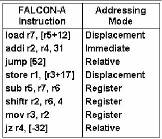
Addressing
Modes
This
table lists the addressing
mode for each instruction
given in the previous
example.
Page
172
Last
Modified: 01-Nov-06
Table of Contents:
- Computer Architecture, Organization and Design
- Foundations of Computer Architecture, RISC and CISC
- Measures of Performance SRC Features and Instruction Formats
- ISA, Instruction Formats, Coding and Hand Assembly
- Reverse Assembly, SRC in the form of RTL
- RTL to Describe the SRC, Register Transfer using Digital Logic Circuits
- Thinking Process for ISA Design
- Introduction to the ISA of the FALCON-A and Examples
- Behavioral Register Transfer Language for FALCON-A, The EAGLE
- The FALCON-E, Instruction Set Architecture Comparison
- CISC microprocessor:The Motorola MC68000, RISC Architecture:The SPARC
- Design Process, Uni-Bus implementation for the SRC, Structural RTL for the SRC instructions
- Structural RTL Description of the SRC and FALCON-A
- External FALCON-A CPU Interface
- Logic Design for the Uni-bus SRC, Control Signals Generation in SRC
- Control Unit, 2-Bus Implementation of the SRC Data Path
- 3-bus implementation for the SRC, Machine Exceptions, Reset
- SRC Exception Processing Mechanism, Pipelining, Pipeline Design
- Adapting SRC instructions for Pipelined, Control Signals
- SRC, RTL, Data Dependence Distance, Forwarding, Compiler Solution to Hazards
- Data Forwarding Hardware, Superscalar, VLIW Architecture
- Microprogramming, General Microcoded Controller, Horizontal and Vertical Schemes
- I/O Subsystems, Components, Memory Mapped vs Isolated, Serial and Parallel Transfers
- Designing Parallel Input Output Ports, SAD, NUXI, Address Decoder , Delay Interval
- Designing a Parallel Input Port, Memory Mapped Input Output Ports, wrap around, Data Bus Multiplexing
- Programmed Input Output for FALCON-A and SRC
- Programmed Input Output Driver for SRC, Input Output
- Comparison of Interrupt driven Input Output and Polling
- Preparing source files for FALSIM, FALCON-A assembly language techniques
- Nested Interrupts, Interrupt Mask, DMA
- Direct Memory Access - DMA
- Semiconductor Memory vs Hard Disk, Mechanical Delays and Flash Memory
- Hard Drive Technologies
- Arithmetic Logic Shift Unit - ALSU, Radix Conversion, Fixed Point Numbers
- Overflow, Implementations of the adder, Unsigned and Signed Multiplication
- NxN Crossbar Design for Barrel Rotator, IEEE Floating-Point, Addition, Subtraction, Multiplication, Division
- CPU to Memory Interface, Static RAM, One two Dimensional Memory Cells, Matrix and Tree Decoders
- Memory Modules, Read Only Memory, ROM, Cache
- Cache Organization and Functions, Cache Controller Logic, Cache Strategies
- Virtual Memory Organization
- DRAM, Pipelining, Pre-charging and Parallelism, Hit Rate and Miss Rate, Access Time, Cache
- Performance of I/O Subsystems, Server Utilization, Asynchronous I/O and operating system
- Difference between distributed computing and computer networks
- Physical Media, Shared Medium, Switched Medium, Network Topologies, Seven-layer OSI Model