 |
Advanced Computer
Architecture-CS501
Advanced
Computer Architecture
Lecture
19
Reading
Material
Vincent
P. Heuring&Harry F. Jordan
Chapter
5
Computer
Systems Design and Architecture
5.1.3
Summary
·
Pipelined
Version of the SRC
·
Adapting
SRC instructions for Pipelined
Execution
·
Control
Signals for Pipelined
SRC
Pipelined
Version of the
SRC
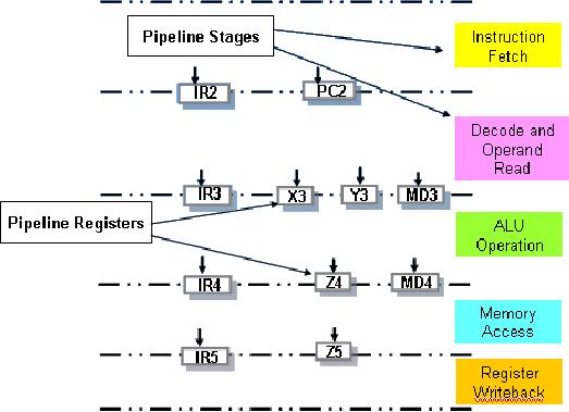
In this
lecture, a pipelined version of
the SRC is presented. The SRC uses a
five-stage
pipeline.
Those five stages are
given below:
1.
Instruction Fetch
2.
Instruction decode/operand fetch
3. ALU
operation
4. Memory
access
5.
Register write
As shown
in the next diagram, there
are several registers between
each stage.
After
the instruction has been
fetched, it is stored in IR2
and
the incremented value of
the
program
counter is held in PC2. When
the register values have
been read, the
first
register
value is stored in X3, and the
second register value is stored in
Y3. IR3
holds
the
opcode
and ra. If it is a store to memory
instruction, MD3
holds
the register value to
be
stored.
After
the instruction has been
executed in the ALU, the
register Z4
holds
the result. The
op-code and ra
are passed on to IR4. During
the write back stage, the
register Z5
holds
the
value to
be stored back into the register,
while the op-code and ra are
passed into IR5.
There
are also two separate
memories and several multiplexers
involved in the
pipeline
operation.
These will be shown at appropriate places in
later figures.
The
number after a particular
register name indicates the
stage where the value of
this
register
is used.
Page
208
Last
Modified: 01-Nov-06
Advanced Computer
Architecture-CS501
Adapting
SRC Instructions for
Pipelined Execution
As
mentioned earlier, the SRC
instructions fall into the
following three categories:
1. ALU
Instructions
2.
Load/Store instructions
3. Branch
Instructions
We will
now discuss how to design a
common pipeline for all
three categories of
instructions.
1. ALU
instructions
ALU
instructions are usually of
the form:
op-code
ra, rb, rc
or
op-code
ra, rb, constant.
In the
diagram shown, X3 and Y3 are
temporary registers to hold the
values between
pipeline
stages. X3 is loaded with operand value
from the register file. Y3
is loaded with
either a
register value from the
register file or a constant
from the instruction.
The
operands
are then available to the
ALU. The ALU function is determined by
decoding the
op-code
bits. The result of the ALU
operation is stored in register Z4, and
then stored in
the
destination register in the
register write back stage.
There is no activity in the
memory
access
stage for ALU instructions.
Note that Z5, IR3,
IR4, and IR5 are not
shown
Page
209
Last
Modified: 01-Nov-06
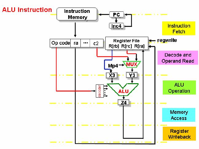
Advanced Computer
Architecture-CS501
explicitly
in the figure. The purpose of
not including these registers is to
keep the
drawing
simple. However, these registers will
transfer values as instructions
progress
through
the pipeline. This comment
also applies to some other figures in
this discussion.
2.
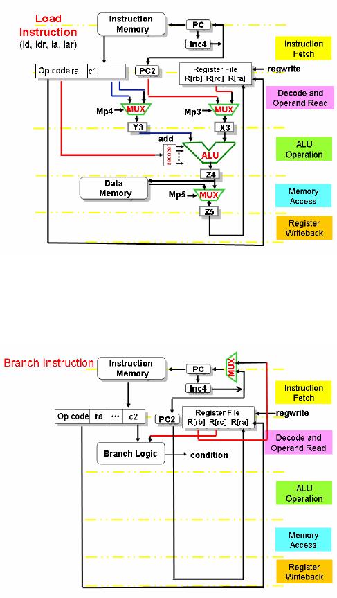
Load/Store instructions
Load/Store
instructions are usually of
the form:
op-code
ra, constant(rb)
The
instruction is loaded into IR2
and
the incremented value of the
PC is loaded in PC2.
In the
next stage, X3
is
loaded with the value in PC2
if
the relative addressing mode
is
used, or
the value in rb
if
the displacement addressing mode is
used. Similarly, C1
is
transferred
to Y3
for
the relative addressing mode, and
c2
is
transferred to Y3
for
the
displacement
addressing mode. The store
instruction is completed once memory
access
has
been made and the memory
location has been written
to. The load instruction
is
completed
once the loaded value is transferred back
to the register file. The
following
figure
shows the schematic for a
load instruction. A similar
schematic can be drawn
for
the store
instruction.
Page
210
Last
Modified: 01-Nov-06
Advanced Computer
Architecture-CS501
3.
Branch Instructions
Branch
Instructions usually involve
calculating the target
address and evaluating a
condition.
The condition is evaluated
based on the c2 field of the
IR and by using the
value in
R[rc]. If the condition is
true, the PC is loaded with
the value in R[rb],
otherwise
it is
incremented by 4 as usual. The
following figure shows these
details.
The
complete pipelined data
path
The
pipelined data path
implementation diagrams shown earlier
for the three SRC
instruction
categories must be combined and
refined to get a working system.
These
details
get complicated very quickly. A
detailed combined diagram is
shown in Figure
5.7 of
the text book.
Page
211
Last
Modified: 01-Nov-06
Advanced Computer
Architecture-CS501
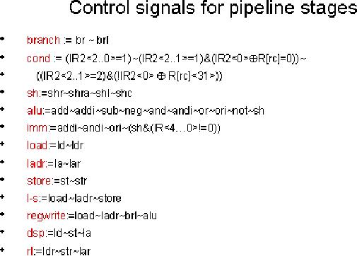
Control
Signals for the Pipelined
SRC
We define
the following signals for
the SRC by grouping similar
op-codes:
In most
cases, the signals defined
above are used in the same
stage where they
are
generated. If
that is not the case, a
number used after the
signal name indicates the
stage
where
the signal is generated.
Using
these definitions, we can develop RTL
statements for describing the
pipeline
activity
as well as the equations for
the multiplexer select signals
for different stages
of
the
pipeline. This is shown in
the next diagram.
Control
Signals for different
pipeline Stages
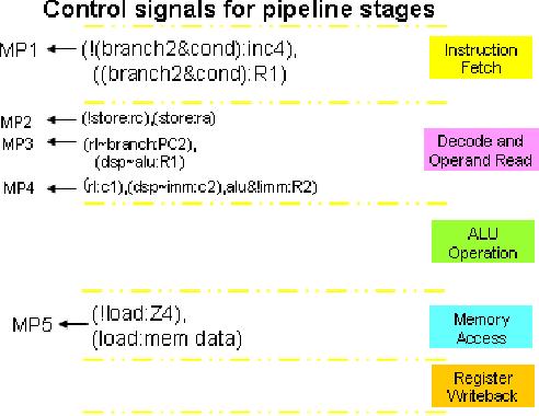
Consider
the RTL description of the
Mp1 signal, which controls
the input to the PC.
It
simply
means that if the branch and
cond signals are not
activated, then the PC
is
incremented
by 4, otherwise if both are
activated then the value of
R1 is copied in to the
PC.
The
multiplexer Mp2 is used to
decide which registers are
read from the register
file. If
the store
signal is activated then
R[rb] from the instruction
bits is read from the
register
file so
that its value may be stored
into memory, otherwise R[rc]
is read from the
register
file.
The
multiplexer Mp3 is used to
decide which registers are
read from the register
file for
operand 2. If
either rl or branch is activated
then the updated value of
PC2 is transferred
to X3,
otherwise if dsp or alu is
activated, the value of
R[ra] from the register
file is
Page
212
Last
Modified: 01-Nov-06
Advanced Computer
Architecture-CS501
transferred
to the x3. In the same
way, multiplexer Mp4 is used
to select an input from
Y3.
In the
same way, multiplexer Mp4 is
used to select an input for
Y3.
The
multiplexer MP5 is used to
decide which value is
transferred to be written back to
the
register file. If the load
signal is activated data
from memory is transferred to
Z5,
however
if the load signal is not
activated then data from Z4
(which is the result of
ALU)
is
transferred to Z5 which is then
written back to the register
file.
Page
213
Last
Modified: 01-Nov-06
Table of Contents:
- Computer Architecture, Organization and Design
- Foundations of Computer Architecture, RISC and CISC
- Measures of Performance SRC Features and Instruction Formats
- ISA, Instruction Formats, Coding and Hand Assembly
- Reverse Assembly, SRC in the form of RTL
- RTL to Describe the SRC, Register Transfer using Digital Logic Circuits
- Thinking Process for ISA Design
- Introduction to the ISA of the FALCON-A and Examples
- Behavioral Register Transfer Language for FALCON-A, The EAGLE
- The FALCON-E, Instruction Set Architecture Comparison
- CISC microprocessor:The Motorola MC68000, RISC Architecture:The SPARC
- Design Process, Uni-Bus implementation for the SRC, Structural RTL for the SRC instructions
- Structural RTL Description of the SRC and FALCON-A
- External FALCON-A CPU Interface
- Logic Design for the Uni-bus SRC, Control Signals Generation in SRC
- Control Unit, 2-Bus Implementation of the SRC Data Path
- 3-bus implementation for the SRC, Machine Exceptions, Reset
- SRC Exception Processing Mechanism, Pipelining, Pipeline Design
- Adapting SRC instructions for Pipelined, Control Signals
- SRC, RTL, Data Dependence Distance, Forwarding, Compiler Solution to Hazards
- Data Forwarding Hardware, Superscalar, VLIW Architecture
- Microprogramming, General Microcoded Controller, Horizontal and Vertical Schemes
- I/O Subsystems, Components, Memory Mapped vs Isolated, Serial and Parallel Transfers
- Designing Parallel Input Output Ports, SAD, NUXI, Address Decoder , Delay Interval
- Designing a Parallel Input Port, Memory Mapped Input Output Ports, wrap around, Data Bus Multiplexing
- Programmed Input Output for FALCON-A and SRC
- Programmed Input Output Driver for SRC, Input Output
- Comparison of Interrupt driven Input Output and Polling
- Preparing source files for FALSIM, FALCON-A assembly language techniques
- Nested Interrupts, Interrupt Mask, DMA
- Direct Memory Access - DMA
- Semiconductor Memory vs Hard Disk, Mechanical Delays and Flash Memory
- Hard Drive Technologies
- Arithmetic Logic Shift Unit - ALSU, Radix Conversion, Fixed Point Numbers
- Overflow, Implementations of the adder, Unsigned and Signed Multiplication
- NxN Crossbar Design for Barrel Rotator, IEEE Floating-Point, Addition, Subtraction, Multiplication, Division
- CPU to Memory Interface, Static RAM, One two Dimensional Memory Cells, Matrix and Tree Decoders
- Memory Modules, Read Only Memory, ROM, Cache
- Cache Organization and Functions, Cache Controller Logic, Cache Strategies
- Virtual Memory Organization
- DRAM, Pipelining, Pre-charging and Parallelism, Hit Rate and Miss Rate, Access Time, Cache
- Performance of I/O Subsystems, Server Utilization, Asynchronous I/O and operating system
- Difference between distributed computing and computer networks
- Physical Media, Shared Medium, Switched Medium, Network Topologies, Seven-layer OSI Model