 |
Control Unit, 2-Bus Implementation of the SRC Data Path |
| << Logic Design for the Uni-bus SRC, Control Signals Generation in SRC |
| 3-bus implementation for the SRC, Machine Exceptions, Reset >> |
Advanced Computer
Architecture-CS501
Advanced
Computer Architecture
Lecture
No. 16
Reading
Material
Vincent
P. Heuring & Harry F. Jordan
Chapter
4
Computer
Systems Design and Architecture
4.2.2,
4.6.1
Summary
·
Control
Signals Generation in SRC
(continued...)
·
The
Control Unit
·
2-Bus
Implementation of the SRC Data
Path
This
section of lecture 16 is a continuation
of the previous
lecture.
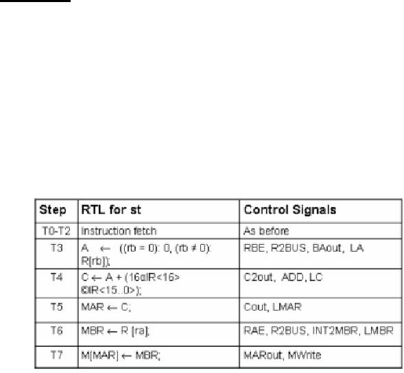
Control
signals for the store
instruction
st
ra, c2(rb)
The store
time step operations are
similar to the load
instruction, with the
exception of
steps T6
and T7. However, one can easily
interpret these now. These
are outlined in the
given
table.
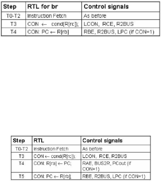
Control
signals for the branch and
branch link instructions
Branch
instructions can be either be simple
branches or link-and-then-branch type.
The
syntax
for the branch instructions
is
brzr
rb, rc
This is
the branch and zero
instruction we looked at earlier.
The control signals for
this
instruction
are:
As usual,
the first three steps
are for the instruction
fetch phase. Next, the
following
control
signals are issued:
Page
185
Last
Modified: 01-Nov-06
Advanced Computer
Architecture-CS501
LCON
to
enable the CON circuitry to operate, and
instruct it to check for the
appropriate
condition
(whether it is branch if zero, or
branch if not equal to zero,
etc.)
RCE
to
allow the register rc value
to be read.
R2BUS
allows
the bus to read from the
selected register.
At step
T4:
RBE
to
allow the register rb value
to be read. rb value is the
branch target
address.
R2BUS
allows
the bus to read from the
selected register.
LPC
(if
CON=1): this control signal
is issued conditionally, i.e.
only if CON is 1, to
enable
the write for the
program counter. CON is set
to 1 only if the specified
condition is
met. In
this way, if the condition
is met, the program counter
is set to the branch
address.
Branch
and link instructions
The
branch and link instruction is
similar to the branch
instruction, with an
additional
step,
T4. Step T4 of the simple
conditional branch instruction
becomes the step T5 in
this
case.
The
syntax of the instruction
`branch and link if zero'
is
brlzr
ra, rb, rc
Table
that lists the RTL and
control signals for the
store instruction of the SRC is
given:
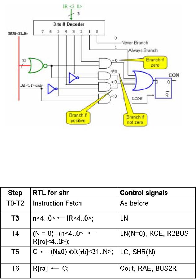
The
circuitry that enables the
condition checking for the
conditional branches in the SRC
is
illustrated in the following
figure:
Page
186
Last
Modified: 01-Nov-06
Advanced Computer
Architecture-CS501
Control
signals for the shift right
instruction
The
given table illustrates the
RTL and the control signals
for the shift right
`shr'
instruction.
This is implemented by applying
the five bits of n (nb4,
nb3, nb2, nb1,
nb0)
to the
select inputs of the barrel
shifter and activating the
control signal SHR as
explained
in an
earlier lecture.
Page
187
Last
Modified: 01-Nov-06
Advanced Computer
Architecture-CS501
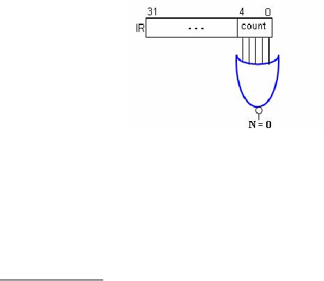
Generating
the Test Condition N=0
The
Control Unit
The
control unit is responsible
for generating control
signals as well as the
timing signals.
Hence
the control unit is
responsible for the
synchronization of internal as well
as
external
events. By means of the
control signals, the control
unit instructs the data
path
what to
do in every clock cycle
during the execution of
instructions.
Control
Unit Design
Since the
control unit performs quite
complex tasks, its design must be done
very
carefully.
Most errors in processor design
are in the Control Unit
design phase. There
are
primarily
two approaches to design a control
unit.
1.
Hardwired approach
2. Micro
programming
Hardwired
approach is relatively faster, however,
the final circuit is quite
complex. The
micro-programmed
implementation is usually slow,
but it is much more
flexible.
"Finite-state
machine" concepts are usually
used to represent the CU.
Every state
corresponds to one
"clock cycle" i.e., 1 state
per clock. In other words
each timing step
could be
considered as just 1 state and therefore
from one timing step to
other timing
step,
the state would change. Now,
if we consider the control
unit as a black box,
then
there
would be four sets of inputs
to the control unit. These
are as follows:
1. The
output of timing step
generator (There are 8
disjoint timing steps in
our
example
T0-T7).
2.
Op-code (op-code is first
given to the decoder and the
output of the decoder
is
given to
the control unit).
3. Data
path generated signals, like
the "CON" control
signal,
4.
Signals from external
events, like "Interrupt"
generated by the Interrupt
generator.
The
complexity of the control is a
function of the
· Number
of states
· Number
of inputs to the CU
· Number
of the outputs generated by
the CU
Page
188
Last
Modified: 01-Nov-06
Advanced Computer
Architecture-CS501
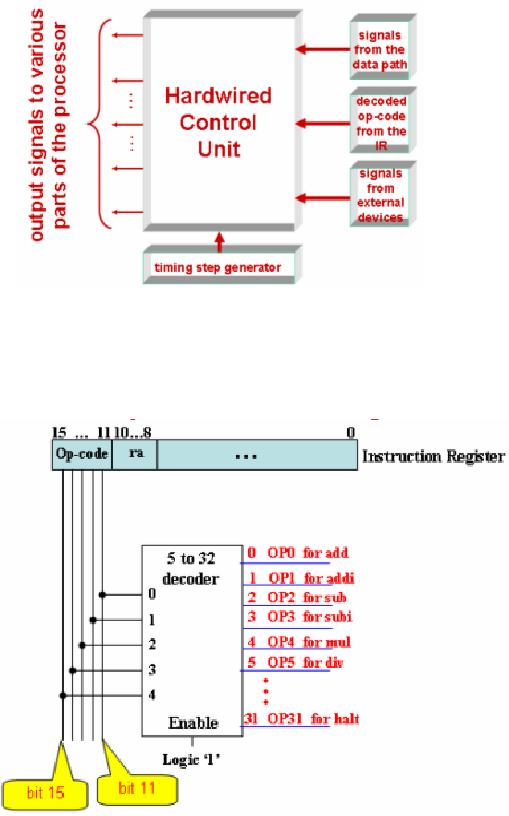
Hardwired
Implementation of the Control
Unit
The
accompanying block diagram
shows the inputs to the
control unit. The output
control
signals
generated from control unit
to the various parts of the
processor are also shown
in
the
figure.
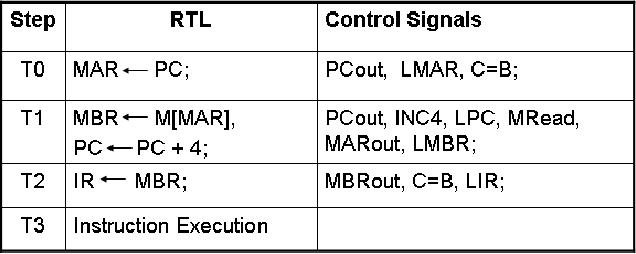
Example
Control Unit for the
FALCON-A
The
following figure shows how
the operation code (op-code)
field of the
Instruction
Register
is decoded to generate a set of
signals for the Control
unit.
This is
an example for the FALCON-A
processor where the
instruction is 16-bit
long.
Similar
concepts will apply to the SRC, in
which case the instruction
word is 32 bits and
IR
<31...27> contains the op-code.
Similar concepts will apply to the
SRC, in which case
Page
189
Last
Modified: 01-Nov-06
Advanced Computer
Architecture-CS501
the
instruction word is 32 bits and
IR<31..27> contains the opcode.
The most significant
5 bits
represent the op-code. These 5-bits from
the IR are fed to a 5-to-32
decoder. These
32
outputs are numbered from
0-to-31 and named as op0, op1 up to op31.
Only one of
these 32
outputs will be active at a given
time .The active output will
correspond to
instruction
executing on the processor.
To design a
control unit, the next
step is to write the Boolean
Equations. For this we
need
to browse
through the structural
descriptions to see which
particular control signals
occur
in
different timing steps. So,
for each instruction we have
one such table
defining
structural
RTL and the control signals
generated at each timing
step. After browsing
we
need to
check that which control
signal is activated under
which condition. Finally
we
need to
write the expression in the
form of a logical expression as
the logical
combination
of "AND" and
"OR" of different control
signals. The given table
shows Boolean
Equations
for some example control
signals.
For
example, PCout would be
active in every T0 timing
step. Then in timing
interval T3
the
output of the PC would be
activated if the op-code is 20 or 22
which represent jump
and
sub-routine call. In step T4 if
the op-code is 16, 17, 18 or
19, again we need
PCout
activated
and these 4 instructions correspond to
the conditional jumps. We can say
that in
other
words in step T1, PCout is
always activated "OR" in T3 it is
activated if the
instruction
is either jump or sub-routine
call "OR" in T4 if there is one of
the conditional
jumps. We
can write an equation for it
as
PCout=T0+T3.(OP20+OP22)+T4.(OP16+OP17+OP18+OP19)
In the
form of logic circuit the
implementation is shown in the
figure. We can see that
we
"OR"
the op-ode 20 and 22 and "AND" it with
T3, then "OR" all
the op16 up to op19
and "AND" it
with T4, then T0 and the
"AND" outputs of T3 and T4 are "OR"
together
to obtain
the PCout.
Page
190
Last
Modified: 01-Nov-06
Advanced Computer
Architecture-CS501
In the
same way the logic
circuit for LPC control
signal is as shown and the
equation
would be
:
LPC=T1+T5.OP20+T6.CON.(OP16+OP17+OP18+OP19)
We can
formulate Boolean equations and
draw logic circuits for
other control signals
in
the
same way.
Effect
of using "real" Gates
We have
assumed so far that the
gates are ideal and that
there is no propagation delay.
In
designing
the control unit, the
propagation delays for the
gates can not be neglected.
In
particular,
if different gates are
cascaded, the output of one
gate forms the input of
other.
The
propagation delays would add
up. This, in turn would
place an upper limit on
the
Page
191
Last
Modified: 01-Nov-06
Advanced Computer
Architecture-CS501
frequency
of the clock which controls
the generation of the timing
intervals T0, T1...
T7.
So, we
can not arbitrarily increase
the frequency of this clock.
As an example consider
the
transfer of the contents of a
register R1 to a register R2.
The minimum time
required
to
perform this transfer is
given by
tmin = tg + tbp + tcomb +
t1
The
details are explained in the
text with reference to Fig
4.10. Thus, the maximum
clock
frequency
based on this transfer will be
1/tmin.
Students are encouraged to study
example
4.1 of
the text.
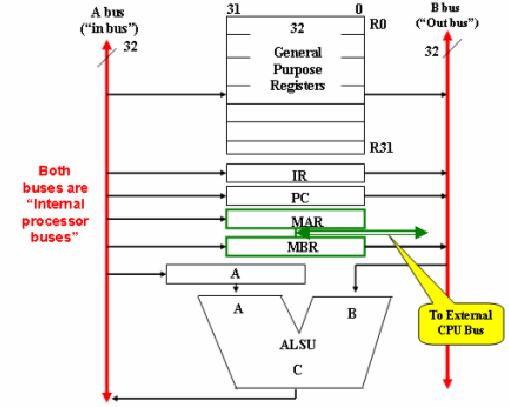
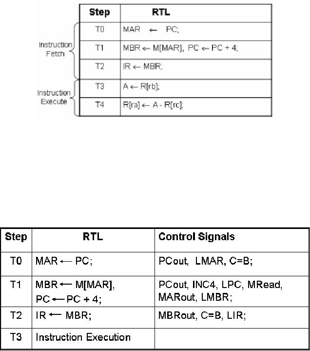
2-Bus
Implementation of the SRC
Data Path
In the
previous sections, we studied the
uni-bus implementation of the
data path in the
SRC.
Now we present a 2-bus implementation of
the data path in the
SRC. We observe
from
this figure that there is a
bus provided for data that
is to be written to a component.
This bus
is named the `in' bus.
Another bus is provided for
reading out the values
from
these
components. It is called the
`out' bus.
Structural
RTL for the `sub' instruction
using the 2-bus data path
implementation
Next, we
look at the structural RTL as
well as the control signals
that are issued in
sequence
for instruction execution in a
2-bus implementation of the
data path. The
given
table
illustrates the Register
Transfer Language representation of
the operations for
carrying
out instruction fetch, and
execution for the sub
instruction.
Page
192
Last
Modified: 01-Nov-06
Advanced Computer
Architecture-CS501
The
first three steps belong to
the instruction fetch phase;
the instruction to be executed
is
fetched
into the Instruction
Register and the PC value is
incremented to point to the
next-
in-line
instruction. At step T3, the
register R[rb] value is
written to register A. At the
time
step
T4, the subtracted result
from the ALSU is assigned to
the destination register
R[ra].
Notice
that we did not need to
store the result in a temporary
register due to the
availability
of two buses in place of one. At
the end of this sequence,
the timing step
generator
is initialized to T0.
Control
signals for the fetch
operation
The
control signals for the
instruction fetch phase are
shown in the table. A
brief
explanation
is given below:
At time
step T0, the
following control signals
are issued:
· PCout: This
will enable read of the Program
Counter, and so its value will
be
transferred
onto the `out' bus
· LMAR: To enable
the load for MAR
· C=B:
This
instruction is used to copy
the value on the `out' bus
to the `in' bus, so
it can be loaded
into the Memory Address
Register. We can observe in the
data-
path
implementation figure given
earlier that, at any time,
the value on the
`out'
bus makes
up the operand B for the
ALSU. The result C of ALSU
is connected to
the
"in" bus, and therefore, the
contents transfer from one bus to
the other can
take
place.
Page
193
Last
Modified: 01-Nov-06
Advanced Computer
Architecture-CS501
At
time step T1:
· PCout:
Again,
this will enable read of the
Program Counter, and so its
value will
be
transferred onto the CPU
internal `out' bus
· INC4:
To
instruct the ALSU to perform
the increment-by-four
operation.
· LPC:
This
control signal will enable write of
the Program Counter, thus
the new,
incremented
value can be written into
the PC if it is made available on
the "in"
bus.
Note that the ALSU is
assumed to include an INC4
function.
· MRead:
To
enable memory word
read.
· MARout:
To
supply the address of memory
word to be accessed by allowing
the
contents
of the MAR (memory address
register) to be written onto
the CPU
external
(address) bus.
· LMBR:
The
memory word is stored in the
register MBR (memory
buffer
register)
by applying this control
signal to enable the write of
the MBR.
At
time step T2:
· MBRout:
The
contents of the Memory
Buffer Register are read
out onto the
`out'
bus, by means of applying
this signal, as it enables
the read for the
MBR.
· C=B:
Once
again, this signal is used to
copy the value from
the `out' bus to the
`in'
bus, so it can be loaded into the
Memory Address Register.
· LIR:
This
instruction will enable the write of
the Instruction Register.
Hence the
instruction
that is on the `in' bus is loaded
into this register.
At time
step T3, the execution
may begin, and the control
signals issued at this
stage
depend on
the actual instruction
encountered. The control
signals issued for
the
instruction
fetch phase are the
same for all the
instructions.
Note
that, we assume the memory
to be fast enough to respond during a
given time slot.
If that
is not true, wait states
have to be inserted. Also
keep in mind that the
control
signals
during each time slot
are activated simultaneously,
while those for
successive
time
slots are activated in
sequence. If a particular control
signal is not shown, its
value is
zero.
Page
194
Last
Modified: 01-Nov-06
Table of Contents:
- Computer Architecture, Organization and Design
- Foundations of Computer Architecture, RISC and CISC
- Measures of Performance SRC Features and Instruction Formats
- ISA, Instruction Formats, Coding and Hand Assembly
- Reverse Assembly, SRC in the form of RTL
- RTL to Describe the SRC, Register Transfer using Digital Logic Circuits
- Thinking Process for ISA Design
- Introduction to the ISA of the FALCON-A and Examples
- Behavioral Register Transfer Language for FALCON-A, The EAGLE
- The FALCON-E, Instruction Set Architecture Comparison
- CISC microprocessor:The Motorola MC68000, RISC Architecture:The SPARC
- Design Process, Uni-Bus implementation for the SRC, Structural RTL for the SRC instructions
- Structural RTL Description of the SRC and FALCON-A
- External FALCON-A CPU Interface
- Logic Design for the Uni-bus SRC, Control Signals Generation in SRC
- Control Unit, 2-Bus Implementation of the SRC Data Path
- 3-bus implementation for the SRC, Machine Exceptions, Reset
- SRC Exception Processing Mechanism, Pipelining, Pipeline Design
- Adapting SRC instructions for Pipelined, Control Signals
- SRC, RTL, Data Dependence Distance, Forwarding, Compiler Solution to Hazards
- Data Forwarding Hardware, Superscalar, VLIW Architecture
- Microprogramming, General Microcoded Controller, Horizontal and Vertical Schemes
- I/O Subsystems, Components, Memory Mapped vs Isolated, Serial and Parallel Transfers
- Designing Parallel Input Output Ports, SAD, NUXI, Address Decoder , Delay Interval
- Designing a Parallel Input Port, Memory Mapped Input Output Ports, wrap around, Data Bus Multiplexing
- Programmed Input Output for FALCON-A and SRC
- Programmed Input Output Driver for SRC, Input Output
- Comparison of Interrupt driven Input Output and Polling
- Preparing source files for FALSIM, FALCON-A assembly language techniques
- Nested Interrupts, Interrupt Mask, DMA
- Direct Memory Access - DMA
- Semiconductor Memory vs Hard Disk, Mechanical Delays and Flash Memory
- Hard Drive Technologies
- Arithmetic Logic Shift Unit - ALSU, Radix Conversion, Fixed Point Numbers
- Overflow, Implementations of the adder, Unsigned and Signed Multiplication
- NxN Crossbar Design for Barrel Rotator, IEEE Floating-Point, Addition, Subtraction, Multiplication, Division
- CPU to Memory Interface, Static RAM, One two Dimensional Memory Cells, Matrix and Tree Decoders
- Memory Modules, Read Only Memory, ROM, Cache
- Cache Organization and Functions, Cache Controller Logic, Cache Strategies
- Virtual Memory Organization
- DRAM, Pipelining, Pre-charging and Parallelism, Hit Rate and Miss Rate, Access Time, Cache
- Performance of I/O Subsystems, Server Utilization, Asynchronous I/O and operating system
- Difference between distributed computing and computer networks
- Physical Media, Shared Medium, Switched Medium, Network Topologies, Seven-layer OSI Model