 |
Logic Design for the Uni-bus SRC, Control Signals Generation in SRC |
| << External FALCON-A CPU Interface |
| Control Unit, 2-Bus Implementation of the SRC Data Path >> |
Advanced Computer
Architecture-CS501
Advanced
Computer Architecture
Lecture
No. 15
Reading
Material
Vincent
P. Heuring & Harry F. Jordan
Chapter
4
Computer
Systems Design and Architecture
4.4
Summary
1) Logic
Design for the Uni-bus
SRC
2)
Control Signals Generation in
SRC
Logic
Design for the Uni-bus
SRC
In the
previous sections, we have looked at
both the behavioral and
structural RTL for
the
SRC. We saw that there is a
need for some control
circuitry for ensuring the
proper
and
synchronized functioning of the
components of the data path,
to enable it to carry out
the
instructions that are part
of the Instruction Set
Architecture of the SRC. The
control
unit
components and related signals make up
the control path. In this
section, we will talk
about
· Identifying
the control signals
required
· The
external CPU
interface
· Memory
Address Register (MAR), and Memory
Buffer Register (MBR)
circuitry
· Register
Connections
We will also take a
look at how sign extension
is performed. This study will
help us
understand
how the entire framework
works together to ensure that
the operations of a
simple
computer like the SRC are
carried out in a smooth and
consistent fashion.
Identifying
control signals
For
any of the instructions that
are a part of the
instruction set of the SRC,
there are
certain
control signals required;
these control signals may be
to select the appropriate
function
for the ALU to be performed, to select
the appropriate registers, or
the
appropriate
memory location.
Any
instruction that is to be executed is
first fetched into the
CPU. We look at the
control
signals
that are required for
the fetch operation.
Control
signals for the fetch
operation
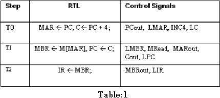
Table 1
lists the control signals
that are needed to ensure
the synchronized
register
transfers
in the instruction fetch
phase. Note that we use
uppercase for control
signals as
we have
been using lowercase for
the instruction mnemonics, and we
want to distinguish
between
the two. Also note
that control signals during
each time slot are
activated
simultaneously,
and that the control signals
for successive time slots
are activated in
sequence.
If a particular control signal is
not shown, its value is
zero.
Page
173
Last
Modified: 01-Nov-06
Advanced Computer
Architecture-CS501
As shown
in the Table: 1, some
control signals are to let
register values to be written
onto
buses, or
read from the buses.
Similarly, some signals are
required to read/ write
memory
contents
onto the bus. The
memory is assumed to be fast
enough to respond during a
given
time slot; if that is not
true, wait states have to be
inserted. We require four
control
signals
to be issued in the time
step T0:
PCout: This
control signal allows the
contents of the Program
Counter register to be
written
onto the internal processor
bus.
LMAR: This
signal enables write onto
the memory address register
(MAR), thus the
value of
PC that is on the bus, is copied
into this register
INC4: It lets
the PC value to be incremented by 4 in
the ALSU, and result to
be
stored in C.
Notice that the value of PC
has been received by the
ALSU as an
operand.
This control signal allows
the constant 4 to be added to
it.
The
ALSU is assumed to include an
INC4 function
LC: This
enables the input to the
register C for writing the
incremented value of PC
onto
it.
During
the time step T1,
the following control
signals are applied:
LMBR: This
enables the "write" for
the register MBR. When
this signal is
activated,
whatever
value is on the bus, can be
written into the
MBR.
MRead: Allow
memory word to be gated from
the external CPU data bus
into the
MBR.
MARout: This
signal enables the tri-state
buffers at the output of
MAR.
Cout: This
will enable writing of the contents of
register C onto the
processor's
internal
data bus.
LPC: This
will enable the input to the PC
for receiving a value that
is currently on the
internal
processor bus. Thus the PC
will receive an incremented
value.
At the
final time step, T2, of
the instruction fetch phase,
the following control
signals
are
issued:
MBRout: To enable
the tri-state buffers with
the MBR.
LIR: To
allow the IR
read
the value from the
internal bus. Thus the
instruction stored
in the
MBR
is
read into the Instruction
Register (IR).
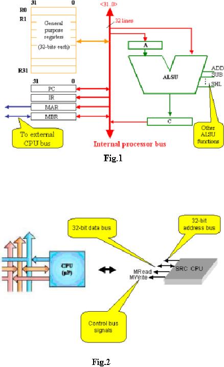
Uni-bus
SRC implementation
The
uni-bus implementation of the SRC
data path is given in the
Fig.1. We can now
visualize
how the control signals in
mutually exclusive time
steps will allow the
coordinated
working of instruction fetch
cycle.
Page
174
Last
Modified: 01-Nov-06
Advanced Computer
Architecture-CS501
Similar
control signals will allow
the instruction execution as
well. We have already
mentioned
the external CPU buses
that read from the
memory and write back to it. In
the
given
figure, we had not shown
these external (address and
data buses) in detail.
Fig.2
will help
us understand this external
interface.
External
CPU bus activity
Let us
take up a sample problem to further enhance
our understanding of the
external
CPU
interface. As mentioned earlier,
this interface consists of the
data bus/ address
bus,
and
control signals for enabling
memory read and
write.
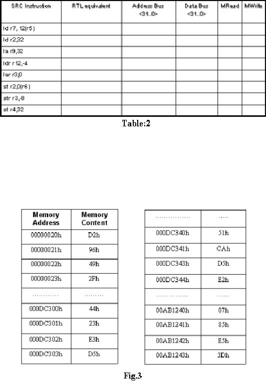
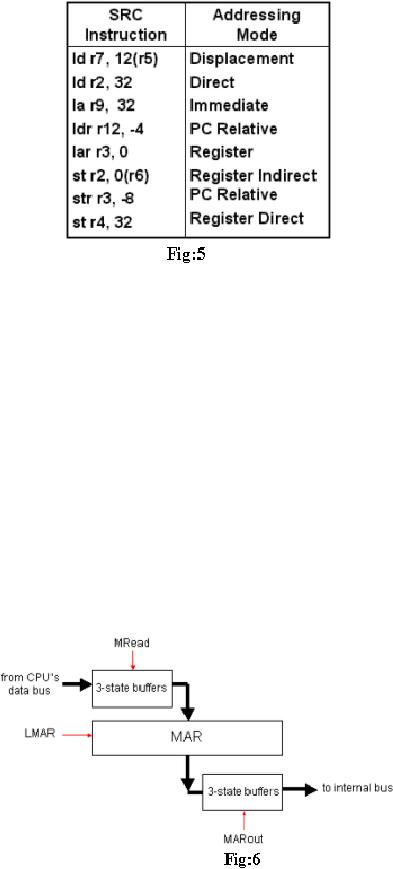
Example
problem:
(a)
What will be the logic
levels on the external SRC
buses when each of the
given SRC
instruction
is executing on the processor?
Complete Table: 2. all
numbers are in the
decimal
number system, unless noted
otherwise.
(b)
Specify memory addressing
modes for each of the SRC
instructions given in Table:
2.
Page
175
Last
Modified: 01-Nov-06
Advanced Computer
Architecture-CS501
Assumptions:
· All
memory content is aligned
properly.
In other
words, all the memory
accesses start at addresses
divisible by 4.
Value in
the PC = 000DC348h
Memory
map with assumed
values
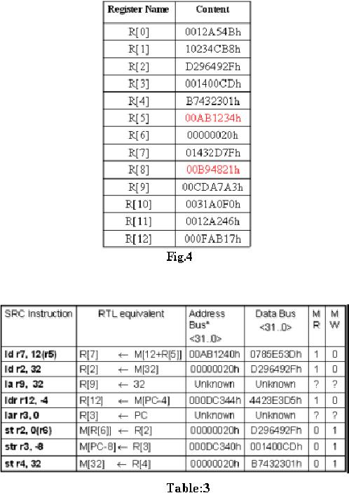
Register
map with assumed
values
Page
176
Last
Modified: 01-Nov-06
Advanced Computer
Architecture-CS501
Solution
Part (a):
(Note
that the SRC uses the
big-endian storage
format).
Solution
part (b):
Page
177
Last
Modified: 01-Nov-06
Advanced Computer
Architecture-CS501
Notes:
*
Relative
addressing is always PC relative in
the SRC
***
Displacement
addressing mode is the same as
Based or Indexed in the SRC.
It is
also the
same as Register Relative
addressing mode
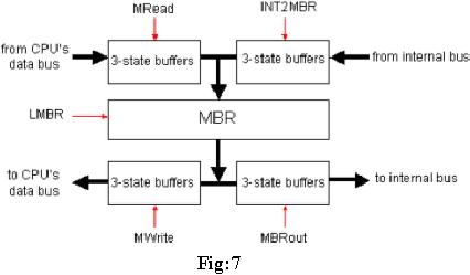
Memory
address register
circuitry
We have
already talked about the
functionality of the MAR.
It
provides a temporary
storage
for the address of memory
location to be accessed. We now take a
detailed look
at how it
is interconnected with other
components. The MAR is connected
directly to the
CPU
internal bus, from which it
is loaded (receives a value). The LMAR
signal causes
the
contents of the internal CPU
bus to be loaded into the MAR. It writes
onto the CPU
external
address bus. The MARout
signal causes the contents
of the MAR to be placed on
the
address bus. Thus, it
provides the addresses for
the memory and I/O devices over
the
CPU's
address bus. A set of
tri-state buffers is provided
with these connections; the
tri-
state
buffers are controlled by
the control signals, which
in turn are issued when
the
corresponding
instruction is decoded. The
whole circuitry is shown in
Fig.6.
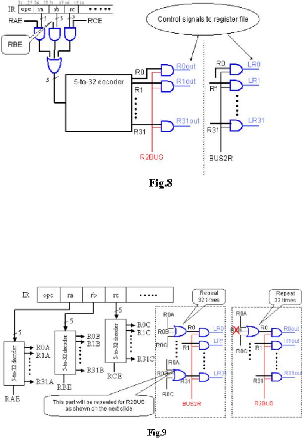
Memory
buffer register
circuitry
The
Memory Buffer Register (MBR)
holds the value read
from the memory or
I/O
device.
It is possible to load the MBR from
the internal CPU bus or from
the external
Page
178
Last
Modified: 01-Nov-06
Advanced Computer
Architecture-CS501
CPU
data bus. The MBR also
drives the internal CPU bus
as well as the external
CPU
data
bus. Similar to the MAR
register, tri-state buffers
are provided at the
connection
points of
the MBR, as illustrated in
the Fig.7.
Register
connections
The
register file containing the
General Purpose Registers is programmer
visible.
Instructions
may refer to any of these
registers, as source operands in an operation or
as
the
destination registers. Appropriate
circuitry is needed to enable the
specified register
for read/
write. Intuitively, we can tell
that we require connections of
the register to the
CPU
internal bus, and we need
control signals that will enable
specified registers to be
read/
write enabled as a corresponding
instruction is decoded. Fig.8
illustrates the
register
connections
and the control signals
generation in the uni-bus
data path of the SRC.
We
can see
from this figure that
the ra, rb and rc fields of
the Instruction Register
specify the
destination
and source registers. The control signals
RAE, RBE and RCE can be
applied
to select
any of the ra, rb or rc
field respectively to apply
its contents to the input of
5-to-
32 decoder.
Through the decoder, we get the
signal for the specific
register to be
accessed.
The BUS2R control signal is
activated if it is desired to write
into the register.
On the
other hand, if the register
contents are to be written to
the bus, the control
signal
R2BUS is
activated.
Page
179
Last
Modified: 01-Nov-06
Advanced Computer
Architecture-CS501
Alternate
control circuitry for
register selection
Fig.9
illustrates an alternate circuitry
that implements the register
connections with the
internal
processor bus, the
instruction register fields, and
the control signals required
to
coordinate
the appropriate read/write
for these registers. Note
that this implementation
is
somewhat
similar to our earlier
implementation with a few
differences. It illustrates
the
fact
that the implementations we
have presented are not
necessarily the only
solutions,
and that
there may be other
possibilities.
In this
alternate circuitry, there is a
separate 5-to-32 decoder for
each of the register
fields
of the
instruction register. The
output of these decoders is
allowed to be read out
and
enables
the decoded register, if the
control signal (RAE, RBE or
RCE) is active.
Page
180
Last
Modified: 01-Nov-06
Advanced Computer
Architecture-CS501
Control
signals Generation in
SRC
We take a
few example instructions to
study the control signals
that are required in
the
instruction
execution phase.
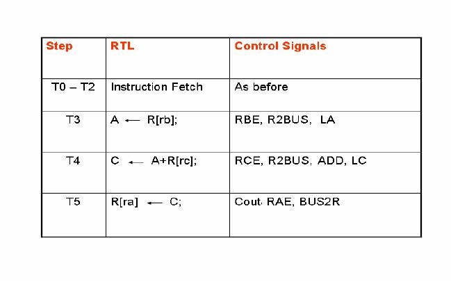
Control
signals for the add
instruction
The
add instruction has the
following syntax:
add
ra, rb, rc
Table: 4
lists the control signals
that are applied at each of
the time steps. The
first three
steps
are of the instruction fetch
phase, and we have already
discussed the control
signals
applied
at this phase.
Table:
4
At time
step T3, the control
RBE is applied, which will enable
the register rb to write
its
contents
onto the internal CPU
bus, as it is decoded. The
writing from the register
onto
the bus
is enabled by the control signal
R2BUS. Control signal LA
allows the bus
contents
to be transferred to the register A
(which will supply it to the
ALSU). At time
step
T4, the control signals
applied are RCE, R2BUS,
ADD, LC, to respectively
enable
the
register rc, enable the
register to write onto the
internal CPU bus (which will
supply
the
second operand to the ALSU
from the bus), select the
add function of the
ALSU
(which
will add the values) and enable
register C (so the result of
the addition
operation
is stored in
the register C). Similarly
in T5, signals Cout, RAE and
BUS2R are activated.
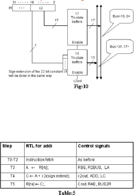
Sign
extension
When we
copy constant values to registers
that are 32 bits wide, we
need to sign extend
the
values first. These values
are in the 2's complement
form, and to sign-extend
these
values,
we need to copy the most
significant bit to all the
additional bits in the
register.
Page
181
Last
Modified: 01-Nov-06
Advanced Computer
Architecture-CS501
We
consider the field c2,
which is a 17 bit constant.
Sign extension of c2 requires
that we
copy
c2<16> to all the
left-most bits of the
destination register, in addition to
copying the
original
constant values to the
register. This means that
bus<31...17> should be the
same
as
c2<16>. A 15 line tri-state
buffer can perform this sign
extension. So we apply
c2<16>
to all
the inputs of this tri-state
buffer as illustrated in the
Fig.10.
Structural
RTL for the addi
instruction
We now
return to our study of the
control signals required in
the instruction
execute
phase. We
have already looked at the
add instruction and the
corresponding signals.
Now
we take a
look at the addi
(add
immediate) instruction, which
has the following
syntax:
addi
ra, rb, c2
Table: 5
lists the RTL and the
control signals for the
addi
instruction:
The
table shows that the
control signals for the addi
instruction are the same as
the add
instruction,
except in the time step
T4. At this time step,
the control signals that
are
applied
are c2out, ADD and LC, to
respectively do the
following:
Enable
the read of the constant c2
(which is sign extended)
onto the internal
processor
bus.
Add the values using
the ALSU and finally assign
the result to register C
by
enabling
write for this
register.
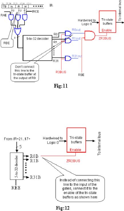
To place
a 0 on the bus
When
the field rb is zero, for
instance, in the load
and
store
instructions,
we need to
place a
zero on the bus. The
given circuit in Fig.11 can be
used to do this.
Page
182
Last
Modified: 01-Nov-06
Advanced Computer
Architecture-CS501
Note
that, by default, the value
of register R0 is 0 in some cases.
So, when the
selected
register
turns out to be 0 (as rb
field is 0), the line
connecting the output of the
register R0
is not
enabled, and instead a hardwired 0 is output
from the tri-state buffer
onto the CPU
internal
bus. An alternate circuitry
for achieving the same is
shown in the Fig.12.
Control
signals for the ld
instruction
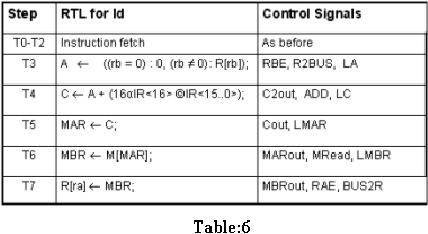
Now we
take a look at the control
signals for the load
instruction.
The syntax of the
instruction
is:
ld
ra, c2 (rb)
Table: 6
outlines the control signals
as well as the RTL for the
load
instruction
in the
SRC.
The
first three steps are of
the instruction fetch phase.
Next, the control signals
issued
are:
Page
183
Last
Modified: 01-Nov-06
Advanced Computer
Architecture-CS501
RBE
is
issued to allow the register
rb value to be read
R2BUS
to
allow the bus to read from
the selected register
LA
to
allow write onto the
register A. This will allow
the CPU bus contents to be
written
to the
register A.
At step
T4 the control signals
are:
c2out
to
allow the sign extended
value of field c2 to be written to
the internal CPU bus
ADD
to
instruct the ALSU to perform
the add function.
LC
to
let the result of the
ALSU function be stored in register C by
enabling write of
register
C.
Control
signals issued at step
T5:
Cout
is to
read the register C, this
copies the value in C to the
internal CPU bus.
LMAR
to
enable write of the Memory Address
Register (which will copy
the value
present on
the bus to MAR). This is the
effective address of memory
location that is to be
accessed
to read (load) the memory
word.
During
the time step
T6:
MARout
to
read onto the external
CPU bus (the address bus, to
be more specific),
the
value
stored in the MAR. This value is an
index to memory location
that is to be
accessed.
MRead
to
enable memory read at the
specified location, this loads
the memory word at
the
specified location onto the
CPU external data
bus.
LMBR
is
the control signal to enable
write of the MBR (Memory
Buffer Register). It
will
obtain its value from
the CPU external data
bus.
Finally,
the control signals issued
at the time step T7
are:
MBRout
is
the control signal to allow
the contents of the MBR to be
read out onto
the
CPU
internal bus.
RAE
is
the control signal for
the destination register
field ra. It will let the
actual index of
the ra
register be encoded, and
BUS2R
will
let the appropriate
destination register be written to
with the value on
the
CPU
internal bus.
Page
184
Last
Modified: 01-Nov-06
Table of Contents:
- Computer Architecture, Organization and Design
- Foundations of Computer Architecture, RISC and CISC
- Measures of Performance SRC Features and Instruction Formats
- ISA, Instruction Formats, Coding and Hand Assembly
- Reverse Assembly, SRC in the form of RTL
- RTL to Describe the SRC, Register Transfer using Digital Logic Circuits
- Thinking Process for ISA Design
- Introduction to the ISA of the FALCON-A and Examples
- Behavioral Register Transfer Language for FALCON-A, The EAGLE
- The FALCON-E, Instruction Set Architecture Comparison
- CISC microprocessor:The Motorola MC68000, RISC Architecture:The SPARC
- Design Process, Uni-Bus implementation for the SRC, Structural RTL for the SRC instructions
- Structural RTL Description of the SRC and FALCON-A
- External FALCON-A CPU Interface
- Logic Design for the Uni-bus SRC, Control Signals Generation in SRC
- Control Unit, 2-Bus Implementation of the SRC Data Path
- 3-bus implementation for the SRC, Machine Exceptions, Reset
- SRC Exception Processing Mechanism, Pipelining, Pipeline Design
- Adapting SRC instructions for Pipelined, Control Signals
- SRC, RTL, Data Dependence Distance, Forwarding, Compiler Solution to Hazards
- Data Forwarding Hardware, Superscalar, VLIW Architecture
- Microprogramming, General Microcoded Controller, Horizontal and Vertical Schemes
- I/O Subsystems, Components, Memory Mapped vs Isolated, Serial and Parallel Transfers
- Designing Parallel Input Output Ports, SAD, NUXI, Address Decoder , Delay Interval
- Designing a Parallel Input Port, Memory Mapped Input Output Ports, wrap around, Data Bus Multiplexing
- Programmed Input Output for FALCON-A and SRC
- Programmed Input Output Driver for SRC, Input Output
- Comparison of Interrupt driven Input Output and Polling
- Preparing source files for FALSIM, FALCON-A assembly language techniques
- Nested Interrupts, Interrupt Mask, DMA
- Direct Memory Access - DMA
- Semiconductor Memory vs Hard Disk, Mechanical Delays and Flash Memory
- Hard Drive Technologies
- Arithmetic Logic Shift Unit - ALSU, Radix Conversion, Fixed Point Numbers
- Overflow, Implementations of the adder, Unsigned and Signed Multiplication
- NxN Crossbar Design for Barrel Rotator, IEEE Floating-Point, Addition, Subtraction, Multiplication, Division
- CPU to Memory Interface, Static RAM, One two Dimensional Memory Cells, Matrix and Tree Decoders
- Memory Modules, Read Only Memory, ROM, Cache
- Cache Organization and Functions, Cache Controller Logic, Cache Strategies
- Virtual Memory Organization
- DRAM, Pipelining, Pre-charging and Parallelism, Hit Rate and Miss Rate, Access Time, Cache
- Performance of I/O Subsystems, Server Utilization, Asynchronous I/O and operating system
- Difference between distributed computing and computer networks
- Physical Media, Shared Medium, Switched Medium, Network Topologies, Seven-layer OSI Model