 |
| Digital Logic Design |
CS302 -
Digital Logic & Design
Lesson
No. 24
APPLICATIONS OF
EDGE-TRIGGERED D FLIP-FLOP
1. Data
Storage using
D-flip-flop
A Multiplexer
based Parallel-to-Serial converter
needs to have stable
parallel data at its
inputs as it
converts it to serial data.
Latches are used to maintain
stable data at the input
of
the
multiplexer. The time
required to convert Parallel
data to Serial data depends
upon the
number of
parallel bits. A byte
parallel data requires 8-bit
storage and 8 clocks are
required to
convert it
into serial data. The
demerit in a gated D-latch
based circuit is the
extended enable
time.
During the time in which
the D-latches are enabled
data applied at the input of
the
latches
can change. D-latch is said
to work in transparent Mode
when the enable signal
is
activated.
D-latch operates in the
latched mode when the
enable signal is inactive.
The
conversion
should only start when
the enable signal has
been deactivated and the
8-bit data
has
been stored in the latches.
A better and a precise
parallel to serial converter
circuit uses
Edge
triggered D-flip-flops. The
8-bit data to be converted
into serial data is stored
precisely at
the
clock transition. Thus, if
the data changes after
the clock transition it has
no effect on the
data
stored in the D flip-flop.
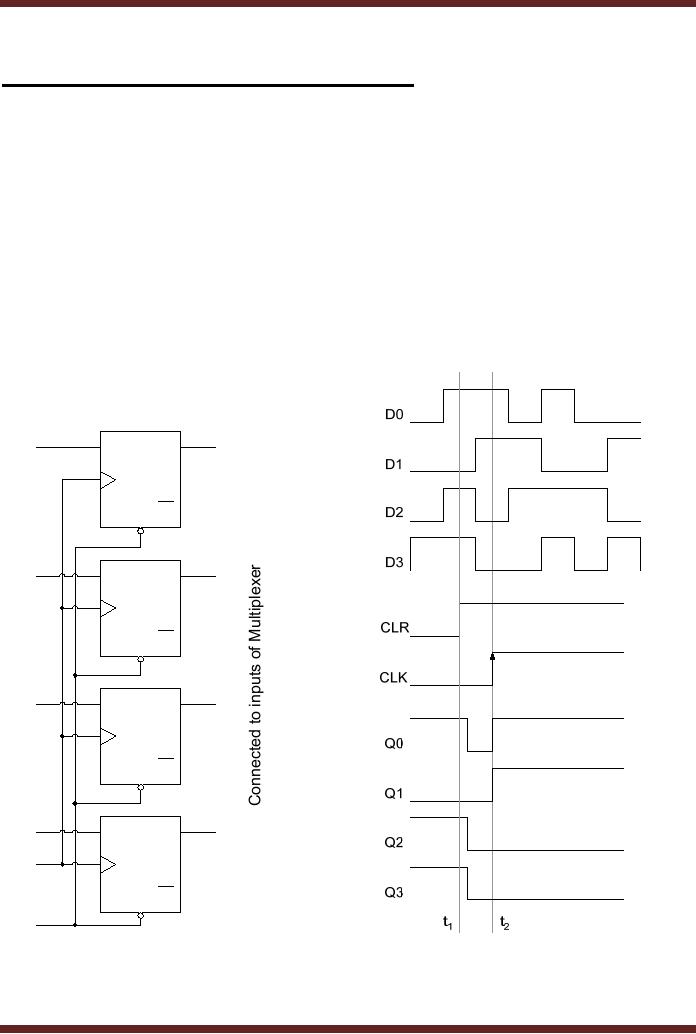
Figure 24.1
D0
Q0
SET
D
Q
Q
CLR
D1
Q1
SET
D
Q
Q
CLR
D2
Q2
SET
D
Q
Q
CLR
D3
Q3
SET
D
Q
CLK
Q
CLR
CLR
Figure
24.1 D-flip-flops used
for Parallel Data
Storage
In the
timing diagram shown the
data at inputs D0, D1, D2
and D3 is constantly
changing. At
interval t1
the
four D-flip-flops are reset
to 0,0,0 and 0 by activating
the clear
244
CS302 -
Digital Logic & Design
input. In
the timing diagram the
outputs of the four D
flip-flops are shown set to
logic zero after
a slight
delay. At interval t2 the clock transition
from logic low to logic
high latches in the in
the
data at
the inputs of the four D
flip-flops. The Q output of
all the four latches
remains stable
after
interval t1.
Changes at the D inputs of
the four latches do not
change the Q outputs of
the
flour D
flip-flops.
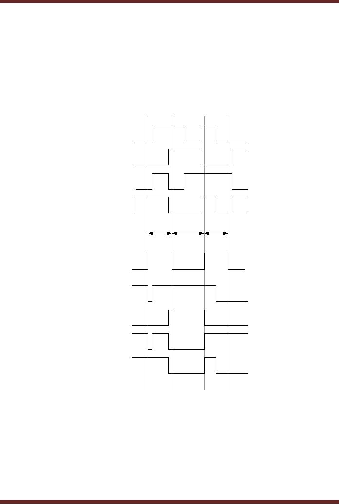
In the
transparent Mode, the
changes in the data applied
at the inputs of the latch
are
seen at
the output of the latch,
where as in the latched mode
changes in the input data
are not
reflected at
the output. Figure
24.2
D0
D1
D2
D3
transparent
transparent
latched
CLK
Q0
Q1
Q2
Q3
t2
t3
t4
t1
Figure
24.2
Timing
diagram of D-Latch
2. Synchronizing
Asynchronous inputs using D
flip-flop
In synchronized
digital systems all the
circuits change their state
with respect to a
common
clock and all the
input and output signals
are synchronized. However,
external inputs
that
are applied to digital
circuits through switches
and keypads are not
synchronized with the
clock.
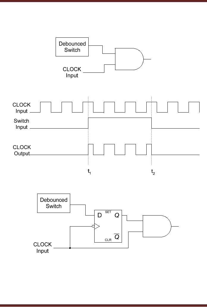
The asynchronous inputs can
occur at any instant of
time. Consider the circuit
based on
a 2-input AND
gate which has a clock
signal connected to one of
its inputs and the
other input
is connected to
an input de-bounced switch.
Figure 24.3. An asynchronous
input applied
through
the switch can cause
incomplete or partial pulses at
the output of the AND
gate.
245
CS302 -
Digital Logic & Design
Figure
24.4. A D-flip-flop synchronizes
the input asynchronous
signal such that the
output of
the AND
gate has complete clock
pulses. Figure 24.5. The
timing diagram of the
synchronized
input
circuit is shown in figure
24.6.
Figure
24.3
AND Gate
connected to external switch
and clock
Figure
24.4
Timing
Diagram of AND Gate connected to
external switch and
clock
Figure
24.5
D flip-flop
used to synchronize the AND
Gate output
246
CS302 -
Digital Logic & Design
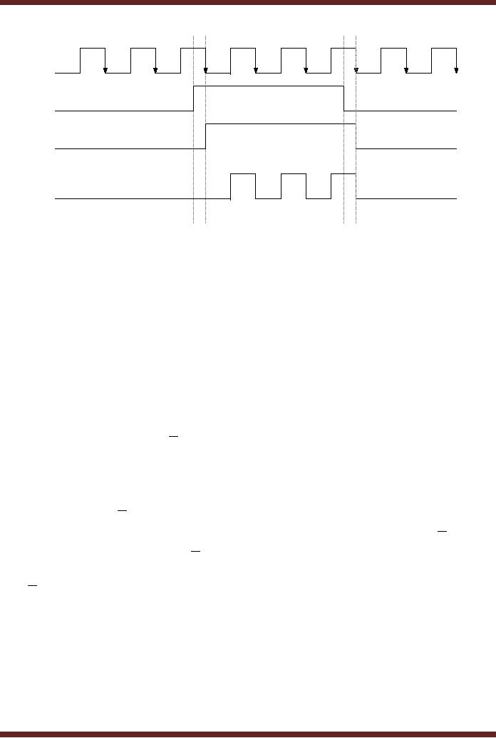
CLOCK
Input
Switch
Input
Q
Output
CLOCK
Output
t1 t2
t3 t4
Figure
24.6
Timing
Diagram of the synchronized
switch input
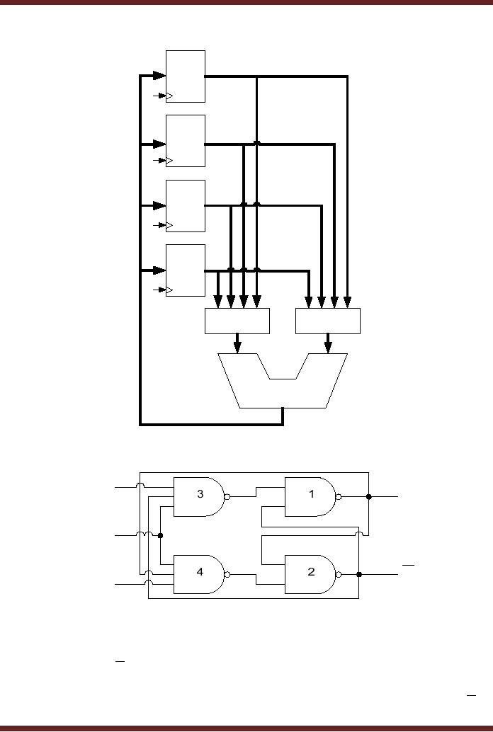
3. Parallel
Data Transfer using D
flip-flop
Microprocessor
use multi-bit flip-flops to
store information. These
multi-bit flip-flops
are
known as
registers. These registers
for example, can store
data generated at the output
of the
ALU.
The registers can also be
used to exchange or copy
data. Figure 24.7. A
register is a set
of flip-flops
connected in parallel to store
multi-bit binary information.
The clock inputs of all
the
flip-flops
are connected together, to
allow simultaneous latching of
the multi-bit input
data.
Edge-Triggered
J-K Flip-flop
The
J-K flip-flop is widely used
in digital circuits. Its
operation is similar to that of
the S-
R flip-flop
except that the J-K
flip-flop doesn't have an
invalid state, instead it
toggles its state.
The
circuit diagram of a J-K
edge-triggered flip-flop is similar to
that of the edge-triggered
S-R
flip-flop
except that the Q and
Q output of
the J-K flip-flop are
connected back to the
input
NAND gates
which have the K and J
inputs respectively. Figure
24.8. The operation of the
J-K
flip-flop
for different combinations of
inputs is described
below.
1. J = 0 and K
=0
With
Q=1 and Q =0, on a
clock transition the outputs
of NAND gates 3 and 4 are
set to
logic 1.
With logic 1 value at the
inputs of NAND gates 1 and 2
the output Q and Q remains
unchanged.
Similarly, with Q=0 and
Q =1, on a
clock transition the outputs
of the NAND gates
3 and 4
are set to logic 1. With
logic 1 value at the inputs
of NAND gates 1 and 2 the
output Q
and Q remains
unchanged. Thus when J=0
and K=0 the previous
state is maintained
and
there is no
change in the output.
247
CS302 -
Digital Logic & Design
8-bit
D
flip-flop
1
Data
Store
1
8-bit
D
flip-flop
2
Data
Store
2
8-bit
D
flip-flop
3
Data
Store
3
8-bit
D
flip-flop
4
Data
Store
4
8-bit
8-bit
4-to-1
MUX
4-to-1
MUX
8-bit
ALU
Figure
24.7
D-flip-flops
used to store data
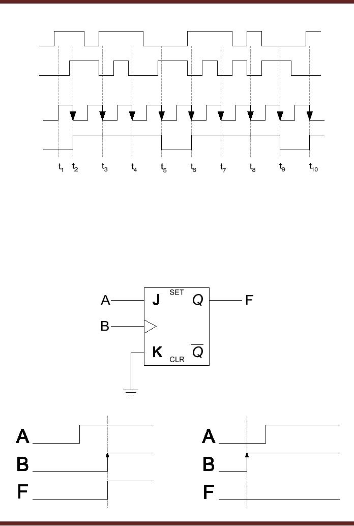
J
Q
CLK
Q
K
Figure
24.8
Edge-triggered
J-K flip-flop
2. J = 0 and K
=1
With
Q=1 and Q =0, on a
clock transition the output
of NAND gate 3 is set to logic
1.
The
output of the NAND gate 4 is
set to 0 as all three of its
inputs are at logic 1. The
logic 1
and 0 at
the inputs of the NAND gates
3 and 4 respectively resets
the Q output to 0 and Q to
248
CS302 -
Digital Logic & Design
1. With
Q=0 and Q
=1, on a
clock transition the output
of NAND gate 3 is set to logic 1.
The
output of
the NAND gate 4 is also set
to 1 as the input of the NAND
gate 4 is connected to
Q=0.
Logic 1 at the inputs of the
NAND gates 3 and 4 respectively
retains the Q and Q to 0
and 1
respectively. Thus when J=0
and K=1 the J-K
flip-flop irrespective of its
earlier state is
rest to
state Q=0 and Q =1.
3. J = 1 and K
=0
With
Q=1 and Q =0, on a
clock transition the output
of NAND gate 4 is set to logic
1.
The
output of the NAND gate 3 is
also set to 1 as its input
connected to Q is at logic 0.
Thus
inputs 1
and 1 at inputs of NAND gates 1
and 2 retain the Q and
Q output to 1
and 0
respectively.
With Q=0 and Q =1, on a
clock transition the output
of NAND gate 4 is set to
logic 1.
The output of the NAND gate
3 is set to 0 as all its
input are at logic 1. Thus
inputs 0
and 1 at
inputs of NAND gates 1 and 2
sets the flip-flop to Q=1
and Q =0.
Thus when J=1
and
K=0
the J-K flip-flop
irrespective of its output
state is set to state Q=1
and Q =0.
4. J = 1 and K
=1
With
Q=1 and Q =0, on a
clock transition the output
of the NAND gates 3 and 4
depend
on the
outputs Q and Q . The
output of NAND gate 3 is set to 1 as
Q is connected to
its input.
The
output of NAND gate 4 is set to 0 as
all its inputs including Q
is at logic 1. A logic 1 and
0
at the
input of gates 1 and 2
toggles the outputs Q and
Q from
logic 1 and 0 to 0 and
1
respectively.
With Q=0 and Q =1, on a
clock transition the output
of NAND gate 3 is set to 0 as
Q and
the output of NAND gate 4 is
set to 1. A logic 0 and 1 at
the input toggles the
outputs Q
and Q from
logic 0 and 1 to 1 and 0
respectively.
In summary
when J-K inputs are
both set to logic 0, the
output remains unchanged.
At
J=0
and K=1 the J-K
flip-flop is reset to Q=0
and Q =1. At
J=1 and K=0 the
flip-flop is set to
Q=1
and Q =0.
With J=1 and K=1
the output toggles from
the previous state. The
truth tables
of the
positive and negative edge
triggered J-K flip-flops are
shown in table 24.1. The
logic
symbols of
the J-K flip-flops are
shown in figure 24.9. The
timing diagrams of the J-K
flip-flops
are
shown in figure
24.10.
J
J
Q
Q
J-K
J-K
CLK
CLK
Flip-Flop
Flip-Flop
K
K
Q
Q
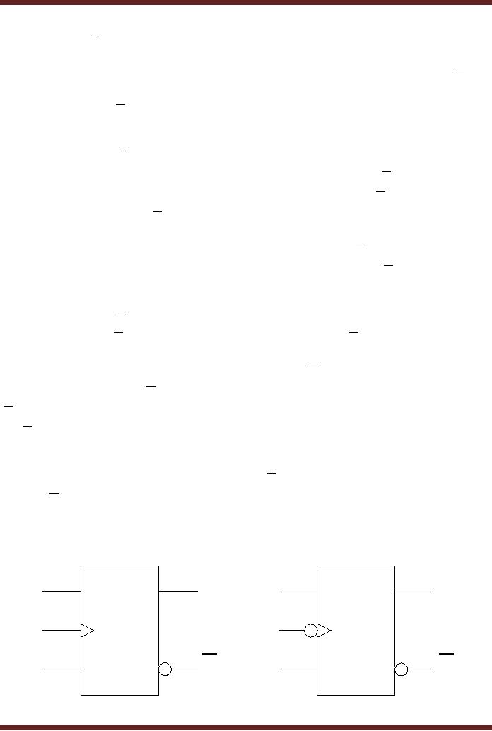
Figure
24.9
Logic
Symbol of Positive and
Negative edge triggered J-K
flip-flops
249
CS302 -
Digital Logic & Design
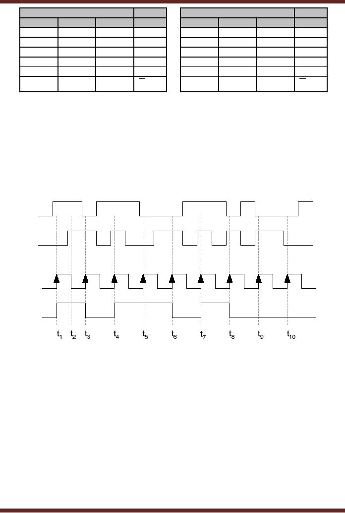
Input
Output
Input
Output
CLK
J
K
Qt+1
CLK
J
K
Qt+1
0
x
X
Qt
0
x
x
Qt
1
x
X
Qt
1
x
x
Qt
↑
0
0
Qt
↓
0
0
Qt
↑
0
1
0
↓
0
1
0
↑
1
0
1
↓
1
0
1
↑
1
1
↓
1
1
Qt
Qt
Table
24.1
Truth-Table of
Positive and Negative Edge
triggered J-K
flip-flops
J
K
CLK
Q
Figure
24.10a Timing diagram of a
Positive Edge triggered J-K
flip-flop
250
CS302 -
Digital Logic & Design
J
K
CLK
Q
Figure
24.10b Timing diagram of a
Negative Edge triggered J-K
flip-flop
Applications of
Edge-Triggered J-K
Flip-flop
1. J-K
flip-flop used as sequence
detector
Some
digital applications require
that the inputs be applied
in a certain sequence to
activate an
output. This is possible
with J-K flip-flops. Figure
24.11
Figure
24.11a J-K flip-flop
connected to respond to a particular
input sequence
Figure
24.11b Timing diagram of the
input sequence
251
CS302 -
Digital Logic & Design
2. J-K
flip-flop used as frequency
divider
In digital
circuit different parts of
the circuit can operate at
different frequencies
obtained
from the master clock
frequency. For example,
three different parts of a
digital
system
might operate at 4 MHZ, 2 MHZ and 1 MHZ
clock frequency respectively.
Same clock
source
should be used (instead of
three separate clock
sources) to maintain
synchronization
between
the three parts. A clock
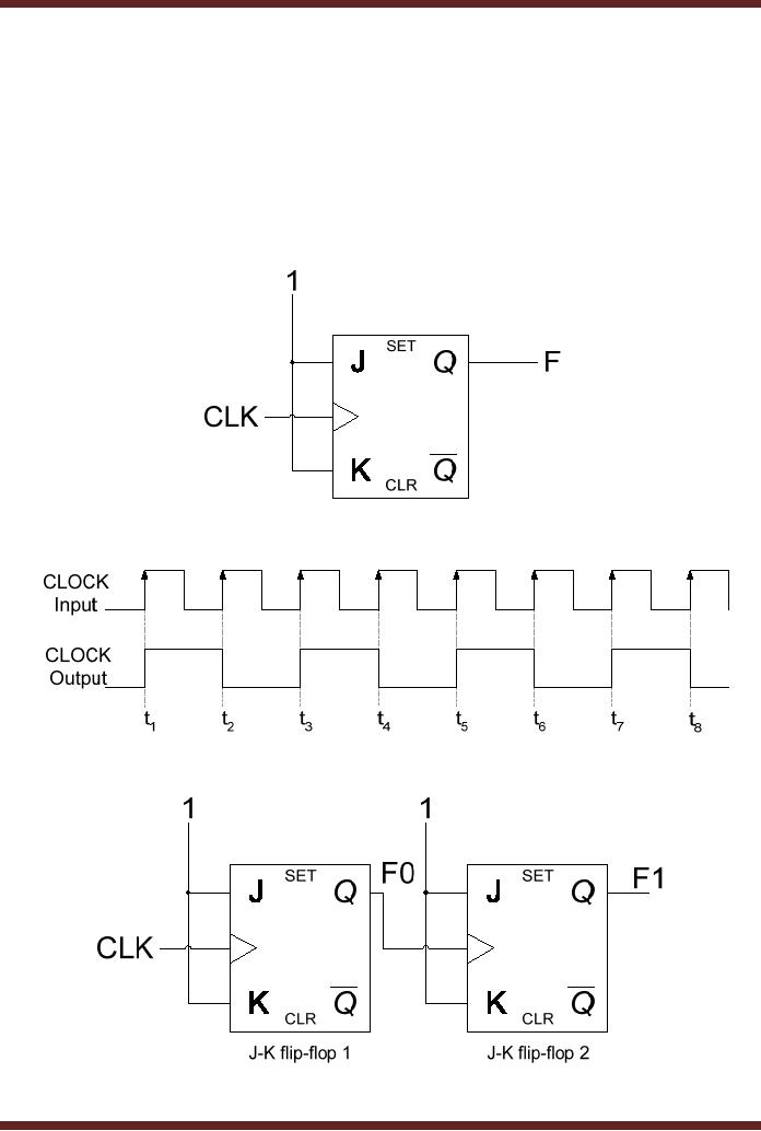
frequency can be divided by 2
using a J-K flip flop.
The J-K
inputs of
the flip-flop are connected
to logic high (1). At each
clock transition the output
of the
flip-flop
toggles to the alternate
state. Figure 24.12. A 4MHz
clock signal can be divided
into 2
MHZ and 1 MHZ
signal using two J-K
flip-flops connected together.
Figure 24.13.
Figure
24.12a J-K flip-flop
connected as frequency
divider
Figure
24.12b Timing diagram of J-K
flip-flop frequency
divider
Figure
24.13a J-K flip-flop
connected as divide-by-4 frequency
divider
252

CS302 -
Digital Logic & Design
CLOCK
Input
F0
Output
F1
Output
t1
t2
t3
t4
t5
t6
t7
t8
Figure
24.13b Timing diagram of J-K
divide-by-4 frequency
divider
3. J-K
flip-flop used as a shift
register
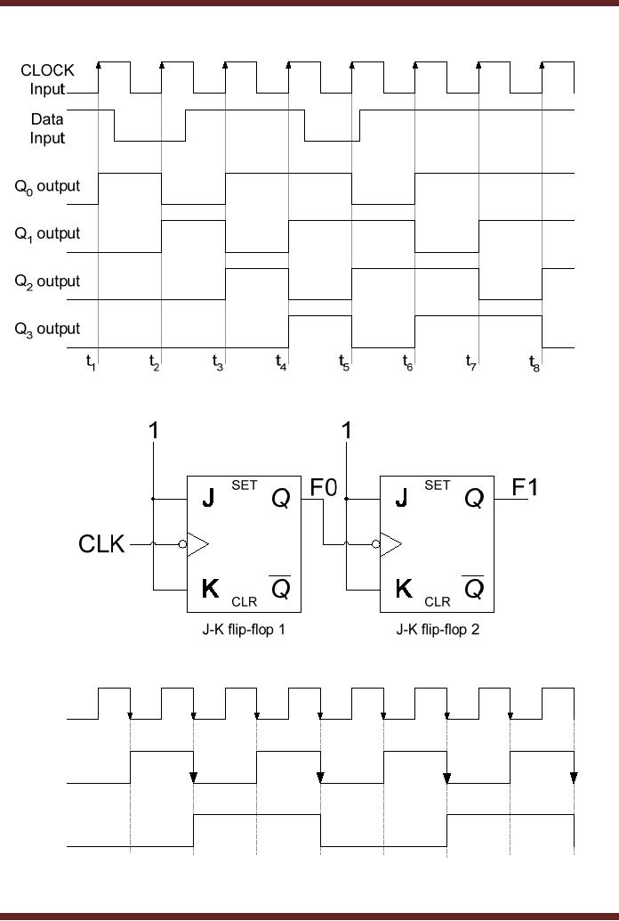
Binary
numbers can be multiplied or
divided by a constant 2 by shifting
the binary
numbers
left or right by 1-bit
respectively. Multiplication and
Division by a factor of 2n, (where n
= 1, 2, 3, 4 ....)
can be achieved by shifting
the binary by n bits to the
left or right
respectively.
Binary
numbers can be easily
shifted in the left or right
direction by using J-K
flip-flop based
shift
registers. figure
24.14.
Figure
24.14a 4-bit right shift
register
4. J-K
flip-flop used as a
counter
Counters
which count up or count down
are commonly used in digital
circuits. An up-
counter
counts up from 0 to 10 increments to
the next higher count
value on the application
of
each
clock signal. Similarly, a
down-counter counts down to
the next lower count
value on the
application of
each clock pulse. Figure
24.15.
253
CS302 -
Digital Logic & Design
Figure
24.14b Timing diagram of a
4-bit right shift
register
Figure
24.15a 2-bit
up-counter
CLOCK
Input
F0
Output
F1
Output
t1
t2
t3
t4
t5
t6
t7
t8
Figure
24.15b Timing diagram of a
2-bit up-counter
254
- AN OVERVIEW & NUMBER SYSTEMS
- Binary to Decimal to Binary conversion, Binary Arithmetic, 1’s & 2’s complement
- Range of Numbers and Overflow, Floating-Point, Hexadecimal Numbers
- Octal Numbers, Octal to Binary Decimal to Octal Conversion
- LOGIC GATES: AND Gate, OR Gate, NOT Gate, NAND Gate
- AND OR NAND XOR XNOR Gate Implementation and Applications
- DC Supply Voltage, TTL Logic Levels, Noise Margin, Power Dissipation
- Boolean Addition, Multiplication, Commutative Law, Associative Law, Distributive Law, Demorgan’s Theorems
- Simplification of Boolean Expression, Standard POS form, Minterms and Maxterms
- KARNAUGH MAP, Mapping a non-standard SOP Expression
- Converting between POS and SOP using the K-map
- COMPARATOR: Quine-McCluskey Simplification Method
- ODD-PRIME NUMBER DETECTOR, Combinational Circuit Implementation
- IMPLEMENTATION OF AN ODD-PARITY GENERATOR CIRCUIT
- BCD ADDER: 2-digit BCD Adder, A 4-bit Adder Subtracter Unit
- 16-BIT ALU, MSI 4-bit Comparator, Decoders
- BCD to 7-Segment Decoder, Decimal-to-BCD Encoder
- 2-INPUT 4-BIT MULTIPLEXER, 8, 16-Input Multiplexer, Logic Function Generator
- Applications of Demultiplexer, PROM, PLA, PAL, GAL
- OLMC Combinational Mode, Tri-State Buffers, The GAL16V8, Introduction to ABEL
- OLMC for GAL16V8, Tri-state Buffer and OLMC output pin
- Implementation of Quad MUX, Latches and Flip-Flops
- APPLICATION OF S-R LATCH, Edge-Triggered D Flip-Flop, J-K Flip-flop
- Data Storage using D-flip-flop, Synchronizing Asynchronous inputs using D flip-flop
- Dual Positive-Edge triggered D flip-flop, J-K flip-flop, Master-Slave Flip-Flops
- THE 555 TIMER: Race Conditions, Asynchronous, Ripple Counters
- Down Counter with truncated sequence, 4-bit Synchronous Decade Counter
- Mod-n Synchronous Counter, Cascading Counters, Up-Down Counter
- Integrated Circuit Up Down Decade Counter Design and Applications
- DIGITAL CLOCK: Clocked Synchronous State Machines
- NEXT-STATE TABLE: Flip-flop Transition Table, Karnaugh Maps
- D FLIP-FLOP BASED IMPLEMENTATION
- Moore Machine State Diagram, Mealy Machine State Diagram, Karnaugh Maps
- SHIFT REGISTERS: Serial In/Shift Left,Right/Serial Out Operation
- APPLICATIONS OF SHIFT REGISTERS: Serial-to-Parallel Converter
- Elevator Control System: Elevator State Diagram, State Table, Input and Output Signals, Input Latches
- Traffic Signal Control System: Switching of Traffic Lights, Inputs and Outputs, State Machine
- Traffic Signal Control System: EQUATION DEFINITION
- Memory Organization, Capacity, Density, Signals and Basic Operations, Read, Write, Address, data Signals
- Memory Read, Write Cycle, Synchronous Burst SRAM, Dynamic RAM
- Burst, Distributed Refresh, Types of DRAMs, ROM Read-Only Memory, Mask ROM
- First In-First Out (FIFO) Memory
- LAST IN-FIRST OUT (LIFO) MEMORY
- THE LOGIC BLOCK: Analogue to Digital Conversion, Logic Element, Look-Up Table
- SUCCESSIVE –APPROXIMATION ANALOGUE TO DIGITAL CONVERTER