 |
CS302 -
Digital Logic & Design
Lesson
No. 26
THE
555 TIMER
The
555 Timer is a versatile and
widely used device which
can be configured as a
mono-stable
One-Shot or as an Astable multivibrator.
An Astable multivibrator is known as
an
Oscillator
which does not have
any stable state. Therefore
it continuously changes from
one
unstable
state to the other without
any external trigger.
Timing
Problem in flip-flop
circuits
In synchronous
digital circuits the output
of one flip-flop is connected to
the input of a
second
flip-flop, either directly or
through logic gates. Both
the flip-flops are triggered
through a
common
clock signal connected to
the clock input of both
the flip-flops. This leads
to a
potential
timing problem as shown in
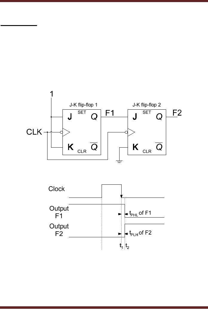
figure 26.1.
Figure
26.1a
J-K
flip-flop circuit with
potential timing
problem
Figure
26.1b
Timing
diagram of J-K flip-flop
circuit with potential
timing problem
Assume
the initial outputs of
flip-flop 1 and 2 are at
logic high and low
respectively.
When
there is a high to low clock
transition t1, the
output of flip-flop 1 toggles to
logic low. The
high to
low clock transition at the
clock input of Flip-flop 2
also occurs at the same
instant t1.
During
the interval t1 and
t2 the output of
flip-flop is changing from
logic high to logic low
and
will go to
logic low after a
propagation delay tPHL.
The input to flip-flop 2 is
changing from logic
high to
low during the time
interval t1
and t2. The input to flip-flop 2
should be held stable for
a
minimum
hold time requirement tH. If the input is not
held stable for tH interval the output
can
265
CS302 -
Digital Logic & Design
not be
guaranteed to be logic high.
Output of flip-flop 2 will be
set to logic high state if
tPHL time
of flip-flop 1
is more than the tH of flip-flop 2. Practically
flip-flops have hold times
that are 5
nsec or
less, most have tH = 0. Therefore, flip-flop
circuits such as the one
shown connected in
the
diagram work
reliably.
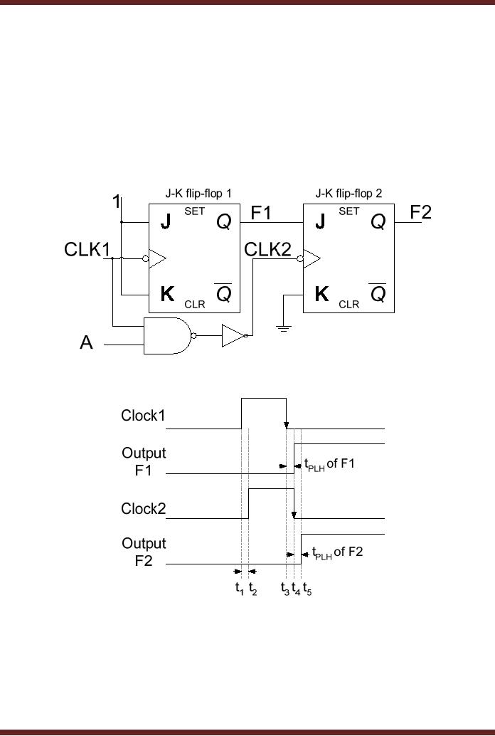
Clock
Skew
One of
the most common problems in
synchronous circuits is `Clock
Skew'. One type
of Clock
Skew occurs when the
same clock signal arrives at
different times at different
clock
inputs to
propagation delay, which
causes different flip-flops to
change states
asynchronously
leading to
unpredictable outputs. Figure
26.2
Figure
26.2a Flip-flop circuit with
potential timing problem due
to Clock Skew
Figure
26.2b
Timing
diagram of J-K flip-flop
circuit with Clock
Skew
In the
circuit diagram both the
flip-flops are connected to
the same clock
signal.
However,
the clock signal to the
second flip-flop is delayed by
the NAND and NOT gates. On
a
high to
low clock transition both
the flip-flops change their
output states assuming that
the
initial
output state of each
flip-flop is logic low. The
Clock Skew is the delay in
the two clock
signals by a
time interval t1 t2 or t3 t4. At
the high to low transition
of clock 1 signal the output
of
F1 toggles
from logic low to logic
high after a propagation
delay of tPLH. If
the propagation
delay of F1 is
less than the clock
skew then at the high to
low clock transition of
clock 2 the J
266
CS302 -
Digital Logic & Design
input of
flip-flop is set to logic
high and at the clock
transition the output F2 is
set to logic high.
If the
propagation delay tPLH of F1
is of a longer duration than
the Clock Skew, the J
input of
the
flip-flop is at logic low at
the high to low transition
of clock 2 the output of F2
remains
unchanged.
Timing
problems occurring due to
clock skew are intermittent
in nature and
therefore
are
difficult to detect. The
clock skew can vary
with changes in temperature,
power supply
voltages,
length of connections and
loading effects. Problems
caused due to clock skew
can
be eliminated by
equalizing clock delays to
different parts of the
circuit.
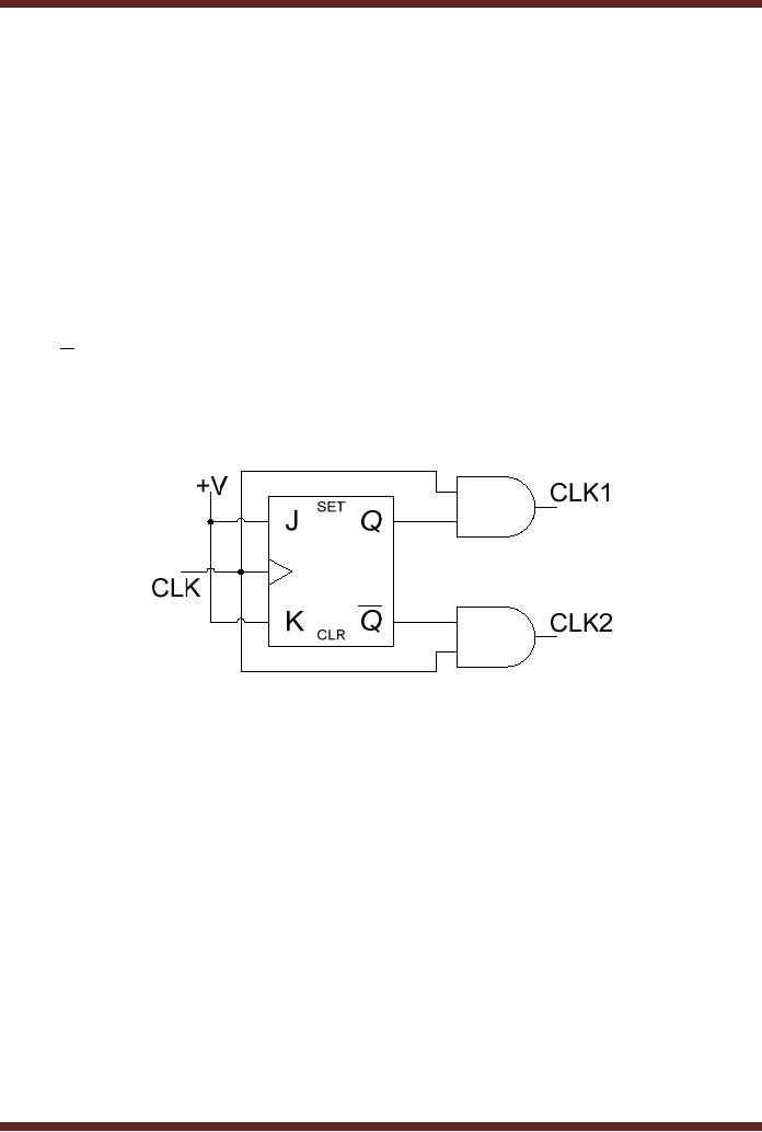
Race
Conditions
Race
conditions are said to occur
when multiple internal
variables change due
to
change in
one input variable.
Depending upon the sequence
in which the internal
variables
change,
the circuit output operates
erratically. Figure 26.3. In
the timing diagram shown, if
the
Q and
Q output
high to low transitions are
slightly delayed, they
coincide with the clock
low to
high
transitions resulting in short
duration pulses which are
difficult to detect. The
glitches due
to race
condition can be avoided by
using a negative-edge triggered
flip-flop instead of
the
positive-edge-triggered
flip-flop used.
Figure
26.3a
J-K
flip-flop circuit with
potential race
condition
267
CS302 -
Digital Logic & Design
Q
Figure
26.3b
Timing
Diagram showing glitches due
to race conditions
Q
Figure
26.3c
Timing
Diagram of negative-edge triggered
flip-flop avoiding
glitches
Counters
Counter
circuits based on flip-flops
are widely used in Digital
Systems. Besides
counting,
these counters are used as
frequency dividers and with
minor changes in the
circuit
268

CS302 -
Digital Logic & Design
they
are used as shift registers.
Counters are classified as
Asynchronous and
Synchronous
counters.
Asynchronous counters as the
name indicates are not
triggered simultaneously.
The
multiple
flip-flops that are
connected together to form a
counter circuit do not
receive the
triggering
clock signal simultaneously.
The flip-flop that
represents the least
significant count
bit of
the n-bit counter is
connected to the clock
signal, the remaining
flip-flops receive
their
clock
signals form the outputs of
the preceding flip-flops
connected in the counter
circuit. The
clock
signal thus ripples through
successive flip-flops. Synchronous
counters on the other
hand
have all the clock
inputs of the multiple
flip-flops connected to a common
clock signal. All
the
flip-flops in a Synchronous counter
receive clock signals
simultaneously.
Asynchronous
and Synchronous are further
classified as up counters or down
counters
depending
upon the sequence in which
they count. They are
further classified in terms of
the
number of
states or the range of
numbers to which the
counters can count.
Asynchronous
Counters (Ripple
Counters)
Asynchronous
counters are implemented by
connecting together multiple
flip-flops
together.
The triggering clock signal
is connected to the clock
input of the first
flip-flop. The
clock
inputs of the remaining
flip-flops are connected to
the Q or Q output of
the previous flip-
flop. On a
clock transition at the
clock input of the first
flip-flop the output state
of the flip-flop
changes.
With the transition in the
output state of the first
flip-flop, there is also a
transition at
the
clock input to the second
flip-flop as the output of
the first flip-flop is
connected to the
clock
input of
the second flip-flop. Due to
the clock transition the
second flip-flop changes its
output
state.
The change in the output
state of the second
flip-flop occurs after the
first flip-flop
changes
its state. Similarly, the
last flip-flop connected in
the counter circuit changes
its output
state
after the output of the
flip-flop connected to its
clock input has changed it
state. The
outputs of
the flip-flops change in a
sequence as the clock signal
propagates through the
flip-
flops as
they change their output
states one after the
other. The Asynchronous
counters are
also
known as Ripple Counters due
to the rippling effect of
the clock signal.
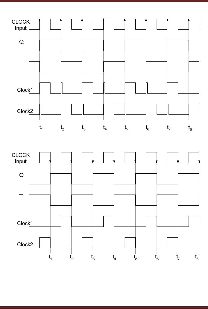
A three-bit
Asynchronous counter circuit is
shown in Figure 26.4. In the
circuit diagram
shown
the Q output of
each is connected to the
clock input of the next
flip-flop. The J-K
inputs
of each of
the three flip-flop are
connected to logic high
allowing the flip-flop to
toggle their
output
state on a high to low
transition at their clock
input.
The
output state of the first
flip-flop toggles at every
positive to negative clock
transition
in intervals
t1 to t8. The
output F1
of the
second flip-flop toggles at
intervals t2, t4, t6 and t8 on
every
high to low transition of
the output F0. The
output F2
toggles
its output state at
intervals t4
and
t8 on a high to low
transition of the flip-flop
output F1.
269
CS302 -
Digital Logic & Design
Figure
26.4a 3-bit Asynchronous
Up-Counter
CLOCK
Input
F0
Output
F1
Output
F2
Output
t1
t2
t3
t4
t5
t6
t7
t8
Figure
26.4b Timing Diagram of a
3-bit Asynchronous
Up-Counter
Input
Output
Clock
F2
F1
F0
Pulses
1
0
0
0
2
0
0
1
3
0
1
0
4
0
1
1
5
1
0
0
6
1
0
1
7
1
1
0
8
1
1
1
Table
26.1
Output
State of a 3-bit Asynchronous
Up-Counter
270
CS302 -
Digital Logic & Design
Propagation
Delay
The
timing diagram shown in
figure 26.4b doesn't take
into account the
propagation
delay
that occurs between each
clock input and the
corresponding toggling output.
The timing
diagram
which takes into account
the propagation delay is
shown in figure 26.5. At
time
interval
t4 on a clock
transition the output F0 toggles to a new state
after a delay determined
by
tPHL propagation delay
of the first flip-flop. At
interval t5
on the
high to low transition of
the F0
output,
the output F1 toggles to a new state
after a propagation delay tPHL of the second
flip-
flop.
Finally, at interval t6 the transition in F1 output toggles the
output F2
of the
third flip-flop.
The
output F2
becomes
stable after a propagation
delay tPLH of
the third flip-flop.
The
propagation
delay of each of the three
flip-flop adds up to delay
the output F2 by
three
propagation
delays with respect to the
clock transition at interval
t4. If the counter
circuit is
extended by
adding more flip-flops, then
the output of the last
flip-flop might exceed the
clock
period of
the clock which causes
timing problems. The
Asynchronous counters can
not work at
high
clock frequencies and cause
problems with decoding
circuits.
CLOCK
Input
F0
Output
F1
Output
F2
Output
t4 t5 t6 t7
t1
t2
t3
Figure
26.5
Timing
Diagram of a 3-bit Asynchronous
with propagation
delay
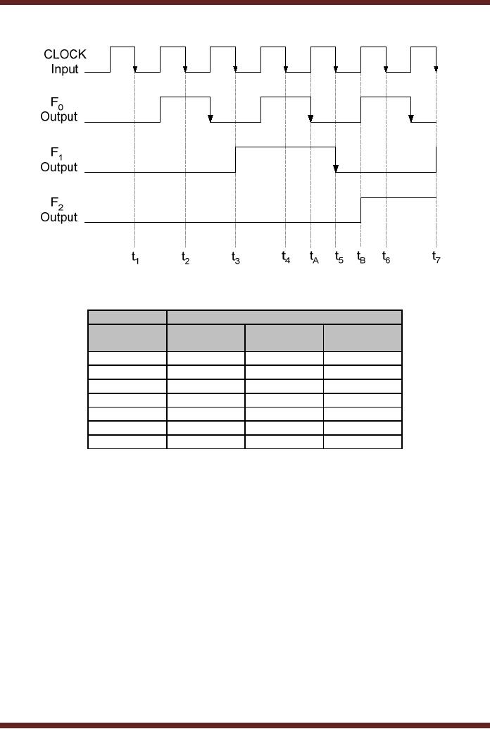
The
timing diagram of the 3-bit
counter circuit using a
clock of a higher frequency
is
shown in
Figure 26.6a. At interval t4, the negative clock
transition toggles the F0 output to logic
low at
interval tA
after a
propagation delay of tPHL. The negative
transition of F0
at tA toggles the
F1 output to logic low at
interval t5
after a
propagation delay of tPHL. Finally, the
F2 output is
toggled to
logic high at interval tB after a delay of tPLH after the
clock (F1)
transition at interval t5.
The
output states of the counter
at intervals t1
to t7 are shown in table
26.2. The output at
interval
t5 should be 100
instead of 010.
271
CS302 -
Digital Logic & Design
Figure
26.6a Timing Diagram of a
3-bit Asynchronous with high
frequency clock
Input
Output
Clock
F2
F1
F0
Pulses
1
0
0
0
2
0
0
1
3
0
1
0
4
0
1
1
5
0
1
0
6
1
0
1
7
1
1
0
Table
26.2
Output of a
3-bit Asynchronous Up-Counter
with high frequency
clock
Mod-n
Counters
The
term Mod represents the
Modulus of the counter which
is the total number
of
unique
states through which the
counter will sequence
through. A 3-bit Asynchronous
counter
can
count up from 0 to 7 or count
down from 7 to 0. The 3-bit
counter has 8 different
states
represented by
the 8 outputs 0 to 7. The
counter states or the range
of numbers of a counter is
determined by
the formula 2m.
where m represents the
number of flip-flops. Therefore, a
Mod-
8 counter
implemented using three
flip-flops 23
has 8
output states.
Counter
can also be designed to have
less number of states than
2m. The
resulting
sequence is
called a truncated sequence.
The counter therefore counts
up to the truncated
sequence.
Designing a truncated sequence
counter is very simple. When
the counter counts
up to the
intended sequence it is reset to
the initial count value 0.
The counter is reset to
the
initial
count value by activating
the Clear asynchronous
inputs. The clears input is
activated by
the
counter through a combinational
circuit that activates its
output when the appropriate
count
sequence is
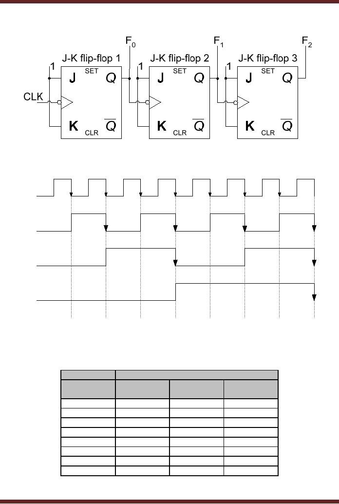
reached. The Mod-6 counter
is shown in figure
26.7.
272
CS302 -
Digital Logic & Design
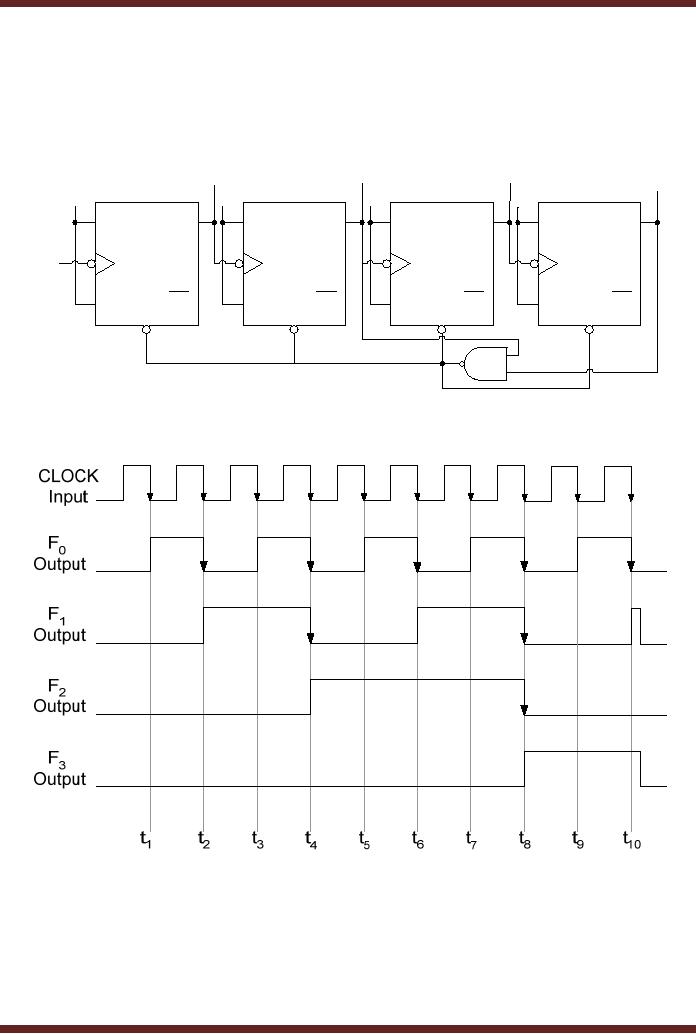
F0
F1
F2
J-K
flip-flop 1
J-K
flip-flop 2
J-K
flip-flop 3
1
1
1
SET
SET
SET
Q
Q
Q
CLK
Q
Q
Q
CLR
CLR
CLR
Figure
26.7a Mod-6 Counter
Figure
26.7b Timing diagram of a
Mod-6 Counter
The
counter counts from state
000 to 101. At interval t6 the counter counts to
110. The
outputs
F1 and F2 of the counter are
connected to the inputs of a
2-input NAND gate,
which
sets
its output to logic zero
when both its inputs
become logic 1 at interval t6. The output of
the
NAND gate is
connected to the three
active-low asynchronous Clear
input of the three
flip-
flops
which are set to low by
the NAND gate. Therefore the
counter is immediately reset
to
state
000 from where it proceeds
to sequence through the
count values. The Mod number
of
the
counter also determines the
frequency at the output of
the counter. The output at
F2 has a
frequency
which is 1/6th of
the input clock frequency.
Thus Mod-n counters can be
design to
generate
1/nth frequency signal
with respect to the input
clock signal.
273
CS302 -
Digital Logic & Design
Mod-10
Counter (Decade
Counter)
A decade
counter uses four-flip-flops to
implement the circuit which
counts up to 10
unique
states (0000 to 1001). The
counter is reset when it
counts to the next state
1010. The
frequency of
the output signal is
1/10th the input
clock frequency. Figure
26.8.
F0
F1
F2
F3
J-K
flip-flop 1
J-K
flip-flop 2
J-K
flip-flop 3
J-K
flip-flop 4
1
1
1
1
SET
SET
SET
SET
Q
J
Q
J
Q
J
Q
J
CLK
Q
K
Q
K
Q
K
Q
K
CLR
CLR
CLR
CLR
Figure
26.8a
Asynchronous
Decade Counter
Figure
26.8b Timing diagram of a
Decode Counter
The
output F1
and
F3 are connected
through a NAND gate to the
active-low clear
inputs
of all
the four flip-flops. The
counter counts from 0000 to
1001 (ten output states),
when it
counts to
1010, the output of the NAND
gate is set to logic low
which resets all the
four flip-
flops to
state 0000.
274
CS302 -
Digital Logic & Design
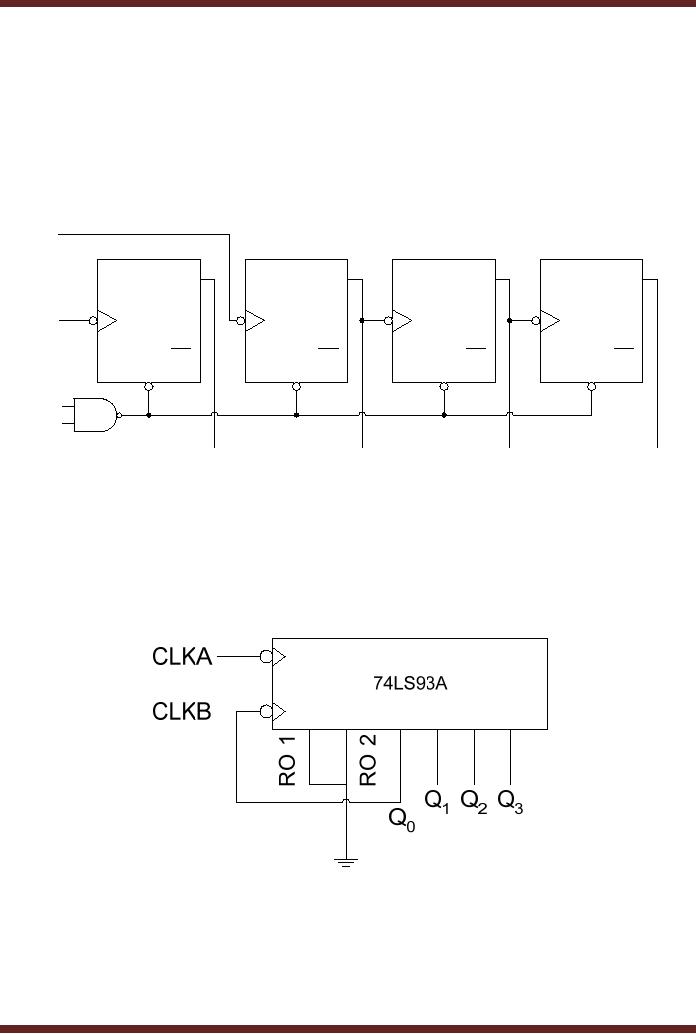
Integrated
Circuit Asynchronous
Counters
Asynchronous
Counters are available in
Integrated Circuit form. The
74LS93A is a 4-bit
Asynchronous
Counter. The counter has
two separate clock inputs
CLK A and CLK B
connected to
the clock input of the
first and second flip-flop
respectively. The second,
third and
fourth
flip-flops are internally
connected as a ripple 3-bit
counter. The counter also
has two
inputs
pins connected to the inputs
of a 2-input NAND (internal) gate,
the output off which
is
connected to
the clear inputs of all
the four flip-flops. The
counter provides four
outputs, one
form
each flip-flop. Figure
26.9
CLK B
SET
SET
SET
SET
Q
J
Q
J
Q
J
Q
J
flip-flop
1
flip-flop
2
flip-flop
3
flip-flop
4
CLK A
Q
K
Q
K
Q
K
Q
K
CLR
CLR
CLR
CLR
RO 1
RO 2
Q0
Q1
Q2
Q3
Figure
26.9
Internal
circuit diagram of the
74LS93A Counter
The
74LS93A can be configured as
MOD-16 counter by connecting
CLK B input pin to
the
Q0 output pin of
the IC. RO 1 and RO 2 are
connected to logic low. A
Decade counter can
be implemented
by connecting CLK B input to
the Q0
and
Q1 and Q3 outputs to RO 1 and
RO
2 respectively.
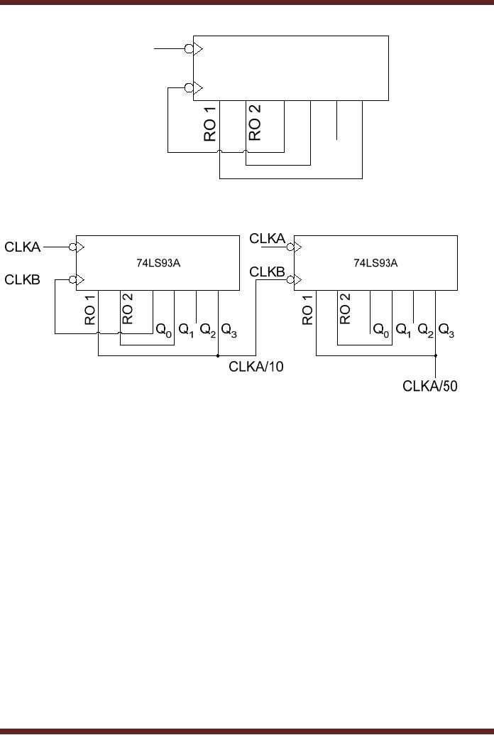
Figure 26.10 Two 74LS
93As ca be cascaded together to
form a larger
counter.
A MOD-50
counter is implemented using
two 74LS93A ICs. Figure
26.11
Figure
26.10a 74LS93A connected as
MOD-16 Counter
275
CS302 -
Digital Logic & Design
CLKA
74LS93A
CLKB
Q0 Q1 Q2 Q3
Figure
26.10b 74LS93A connected as
Decade Counter
Figure
26.11 74LS93A Connected as a
frequency divider (divide by
50)
In the
circuit diagram two 74LS93As
are connected together to
form a frequency
divider
which divides the input
frequency by 50. The first
74LS93A is connected to divide
the
input
frequency by 10. The Q3 output of the first
74LS93A is connected to the
CLKB input of
the
second 74LS93A. The second
74LS93A is connected to divide
the input frequency
at
CLKB by 5.
The Q3 output of the
second 74LS93A therefore
provides an output which is
1/50th
of the
clock applied at the CLKA
input of the first 74LS93A.
The second 74LS93A requires
the
use of
only three flip-flops,
therefore the first
flip-flop with clock input
CLKA is left
unconnected.
276
Table of Contents:
- AN OVERVIEW & NUMBER SYSTEMS
- Binary to Decimal to Binary conversion, Binary Arithmetic, 1s & 2s complement
- Range of Numbers and Overflow, Floating-Point, Hexadecimal Numbers
- Octal Numbers, Octal to Binary Decimal to Octal Conversion
- LOGIC GATES: AND Gate, OR Gate, NOT Gate, NAND Gate
- AND OR NAND XOR XNOR Gate Implementation and Applications
- DC Supply Voltage, TTL Logic Levels, Noise Margin, Power Dissipation
- Boolean Addition, Multiplication, Commutative Law, Associative Law, Distributive Law, Demorgans Theorems
- Simplification of Boolean Expression, Standard POS form, Minterms and Maxterms
- KARNAUGH MAP, Mapping a non-standard SOP Expression
- Converting between POS and SOP using the K-map
- COMPARATOR: Quine-McCluskey Simplification Method
- ODD-PRIME NUMBER DETECTOR, Combinational Circuit Implementation
- IMPLEMENTATION OF AN ODD-PARITY GENERATOR CIRCUIT
- BCD ADDER: 2-digit BCD Adder, A 4-bit Adder Subtracter Unit
- 16-BIT ALU, MSI 4-bit Comparator, Decoders
- BCD to 7-Segment Decoder, Decimal-to-BCD Encoder
- 2-INPUT 4-BIT MULTIPLEXER, 8, 16-Input Multiplexer, Logic Function Generator
- Applications of Demultiplexer, PROM, PLA, PAL, GAL
- OLMC Combinational Mode, Tri-State Buffers, The GAL16V8, Introduction to ABEL
- OLMC for GAL16V8, Tri-state Buffer and OLMC output pin
- Implementation of Quad MUX, Latches and Flip-Flops
- APPLICATION OF S-R LATCH, Edge-Triggered D Flip-Flop, J-K Flip-flop
- Data Storage using D-flip-flop, Synchronizing Asynchronous inputs using D flip-flop
- Dual Positive-Edge triggered D flip-flop, J-K flip-flop, Master-Slave Flip-Flops
- THE 555 TIMER: Race Conditions, Asynchronous, Ripple Counters
- Down Counter with truncated sequence, 4-bit Synchronous Decade Counter
- Mod-n Synchronous Counter, Cascading Counters, Up-Down Counter
- Integrated Circuit Up Down Decade Counter Design and Applications
- DIGITAL CLOCK: Clocked Synchronous State Machines
- NEXT-STATE TABLE: Flip-flop Transition Table, Karnaugh Maps
- D FLIP-FLOP BASED IMPLEMENTATION
- Moore Machine State Diagram, Mealy Machine State Diagram, Karnaugh Maps
- SHIFT REGISTERS: Serial In/Shift Left,Right/Serial Out Operation
- APPLICATIONS OF SHIFT REGISTERS: Serial-to-Parallel Converter
- Elevator Control System: Elevator State Diagram, State Table, Input and Output Signals, Input Latches
- Traffic Signal Control System: Switching of Traffic Lights, Inputs and Outputs, State Machine
- Traffic Signal Control System: EQUATION DEFINITION
- Memory Organization, Capacity, Density, Signals and Basic Operations, Read, Write, Address, data Signals
- Memory Read, Write Cycle, Synchronous Burst SRAM, Dynamic RAM
- Burst, Distributed Refresh, Types of DRAMs, ROM Read-Only Memory, Mask ROM
- First In-First Out (FIFO) Memory
- LAST IN-FIRST OUT (LIFO) MEMORY
- THE LOGIC BLOCK: Analogue to Digital Conversion, Logic Element, Look-Up Table
- SUCCESSIVE APPROXIMATION ANALOGUE TO DIGITAL CONVERTER