 |
SUCCESSIVE APPROXIMATION ANALOGUE TO DIGITAL CONVERTER |
| << THE LOGIC BLOCK: Analogue to Digital Conversion, Logic Element, Look-Up Table |
CS302 -
Digital Logic & Design
Lesson
No. 45
SUCCESSIVE
APPROXIMATION ANALOGUE TO DIGITAL
CONVERTER
The
most commonly used A/D
for converting analogue
values to corresponding
binary
values is
the Successive-Approximation A/D
converter. It has a fixed
conversion time and
is
faster
than the Dual-Slope A/D
converter. The Successive-Approximation
converter is however
slower
than the Flash converter.
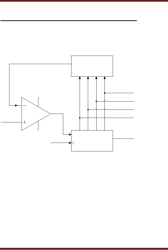
The main components of a
Successive-Approximation A/D
Converter
are the Successive
Approximation Register (SAR), a
Digital to Analogue
Converter
and a
Comparator. Figure
45.1.
Vout
Digital-to-Analogue
Converter
D0
Parallel
Binary
Output
D3
Input
Signal
D
Comparator
SAR
Serial
CLK
Binary
Output
Figure
45.1 Successive-Approximation 4-bit
A/D Converter
The
analogue signal sample which
is to be converted into its
corresponding binary
value is
applied at the non-inverted
input of the Comparator.
Initially, the most-significant
bit D3
is set to
logic 1 by the Successive
Approximation Register (SAR).
The Digital-to-Analogue
converter
converts the binary input
digit 1000 to it equivalent
analogue value. The
output
analogue
value is connected to the
inverted input of the
comparator. If the applied
Input signal
is larger
than the signal generated by
the D/A converter the
output of the comparator is
logic 1
which
sets the most significant
bit D3 of the SAR to
logic 1. The next most
significant bit is
set
to 1 and
the new binary number
1100 is applied at the input
of the D/A converter.
The
analogue
output is applied at the
comparator input which
generates logic 1 or 0
depending
upon
the magnitude of the two
signals applied at the
inputs of the comparator.
Depending
upon
logic 0 or 1 produced at the
output of the comparator,
the SAR sets or resets
the next
most
significant digit. This
procedure is repeated for
all the binary
digits.
Assuming an
analogue signal of 5.2 volts
applied at the input of the
4-bit A/D converter.
Initially,
the SAR sets its 4
bits to 1000, which is
converted to 8 volts by the
D/A converter.
Since
the applied signal (5.2 V)
is less than 8 V signal,
therefore the SAR resets
the most
significant
bit and sets the
next most significant bit
0100. The D/A converts
the 4 bit number to
4 volts
which is less than the
input signal (5.2 V).
The SAR retains the
original bit and sets
the
453
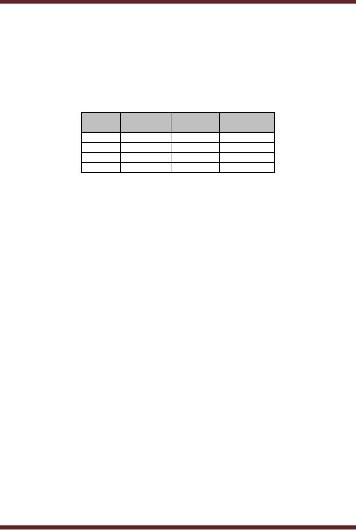
CS302 -
Digital Logic & Design
next
most significant bit.
(0110). The 4-bit number is
converted into an analogue
value of 6
volts by
the D/A converter. Since
the analogue value is
greater than the input
signal therefore
the
SAR resets the bit
and sets the least
significant bit to 1 (0101).
The number is
converted
into an
analogue value by the D/A
converter. The converted
value (5 V) is less than the
input
signal,
therefore the four bits
are retained (0101). Since
the Successive-Approximation
A/D
converter is a
4-bit converter therefore
the 0101 represents the
final value at the end of
the
conversion
process. Table 45.1. The
duration of the conversion
depend upon the
quantization
level, a
6-bit converter completes
its conversion in 6 time
periods.
Vin
SAR
D/A
output
Comparator
output
output
5.2
1000
8
0
5.2
0100
4
1
5.2
0110
6
0
5.2
0101
5
1
Table
45.1
Successive-Approximation
D/A Conversion
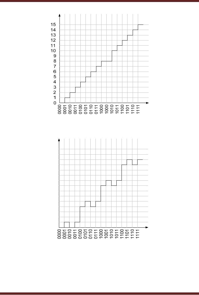
Analogue-to-Digital
Converter Errors
Analogue to
Digital converters exhibit
three different types of
errors during their
conversion
operation. The three errors
encountered during the
conversion operation are
the
Missing
Code, Incorrect Code and
the Offset error. The
three errors are represented
through
graphs.
Figure 45.2. A test signal
which is an ideal linear
ramp is assumed for testing
for the
three
errors.
1. Missing
Code
In the
graph illustrated to highlight
the missing code `1001' a
linearly increasing
analogue
voltage is applied at the
input of an A/D converter
and the binary output is
plotted.
Ideally, a
staircase output should be
obtained showing the
linearly increasing binary
values.
Figure
45.2a. The graph shows a
missing binary code 1001,
represented instead by 1000.
The
missing
code in the case of a Flash
converter is due to the
failure of a comparator which
fails
to provide an
appropriate input to the
Priority Encoder. The
Priority Encoder therefore
outputs
the
same code for analogue
values 8 and 9.
2. Incorrect
Code
Incorrect
Code at the output of the
A/D converter is due to a
particular bit stuck
at
some
fixed logic value. In the
graph illustrating an example of
Incorrect Code, the bit
next to
the
least significant is permanently
stuck at logic 0. Therefore,
for analogue values 2, 3, 6,
7,
10,
11, 14 and 15 the binary
output is 0, 1, 4, 5, 8, 9, 12 and 13
respectively. Figure
45.2b.
454
CS302 -
Digital Logic & Design
Figure
45.2a Missing Code
`1001'
15
14
13
12
11
10
9
8
7
6
5
4
3
2
1
0
Figure
45.2b
Incorrect
Code
3. Offset
Error
The
offset error occurs when
the binary output of the
A/D converter represents a
value
which is
greater than the actual
analogue input signal value.
The error is due to a fault
in the
comparator
circuit. The offset error
can be compensated by adjusting
the output with
respect
to the
amount of offset error. The
missing and incorrect code
however can not be
455

CS302 -
Digital Logic & Design
compensated.
Figure 45.2c. The diagram
illustrates an offset error of 2
volts, as the
corresponding
output value for each
analogue input exceeds by 2
volts.
15
14
13
12
11
10
9
8
7
6
5
4
3
2
1
0
Figure
45.2c Offset Error
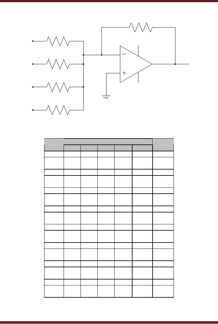
Digital to
Analogue Conversion
Digital
binary signals are converted
into analogue signals using
Digital to Analogue
Converters.
Generally two types of D/A
Converters are used, the
Binary-Weighted-Input D/A
Converter
and R/2R Ladder D/A
Converter.
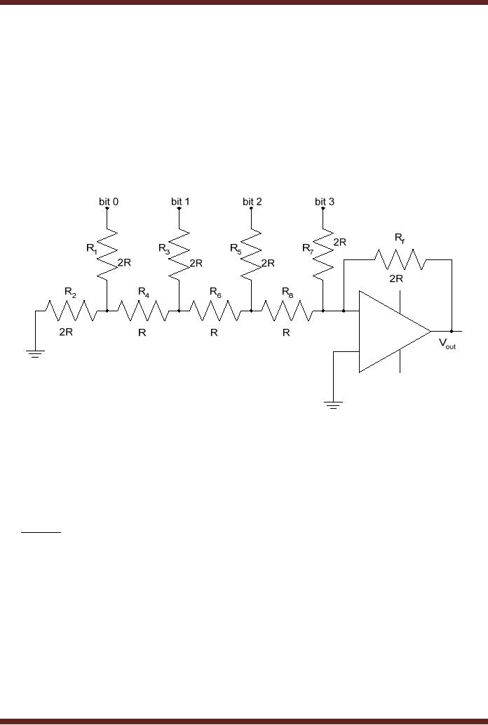
Binary-Weighted-Input
Digital to Analogue
Converter
The
Binary-Weighted-Input D/A converter is
based on a summer circuit
which sums the
input
currents based on the binary
input and represents it as a
voltage output. In the
Binary-
Weighted-Input
Method a resistor network is
used with resistor values
representing the
binary
weights of
the input bits of the
digital code. The binary
(digital input) is applied at
the resistor
inputs. A
current will flow through
the resistor if the input
voltage applied is logic
high. No
current
flows through a resistor if
the input voltage applied is
logic low. The magnitude of
the
current
flowing through each
resistor depends upon the
value of the resistor. The
total current
flowing
through each resistor adds
up and flows through the
feedback resistor Rf which
is
connected
between the output and
the inverting input of the
Op-Amp. The output voltage
of
the
Op-Amp is determined by the
voltage drop across the
Rf resistance. Figure
45.3.
For a
D/A converter with weighted
resistors 8K, 4K, 2K and 1K
respectively and the
feedback
resistor of 2K ohms. The
output voltages for binary
inputs 0000 to 1111 are
shown.
Table
45.2.
456
CS302 -
Digital Logic & Design
Rf
8R
V
bit
0
4R
V
bit
1
Vout
2R
V
bit
2
R
V
bit
3
Figure
45.3
A 4-bit
Binary-Weighted-Input D/A
Converter
Input
Current
through (mA)
Vout
(volts)
R
2R
4R
8R
Rf
0000
0
0
0
0
0
0
0001
0
0
0
0.62
0.625
-1
5
0010
0
0
1.25
0
1.25
-2
0011
0
0
1.25
0.62
1.875
-3
5
0100
0
2.5
0
0
2.5
-4
0101
0
2.5
0
0.62
3.125
-5
5
0110
0
2.5
1.25
0
3.75
-6
0111
0
2.5
1.25
0.62
4.375
-7
5
1000
5
0
0
0
5.0
-8
1001
5
0
0
0.62
5.625
-9
5
1010
5
0
1.25
0
6.25
-10
1011
5
0
1.25
0.62
6.875
-11
5
1100
5
2.5
0
0
7.5
-12
1101
5
2.5
0
0.62
8.125
-13
5
1110
5
2.5
1.25
0
8.75
-14
1111
5
2.5
1.25
0.62
9.375
-15
5
Table
45.2
D/A
Output voltages for binary
inputs 0000 to 1111
457
CS302 -
Digital Logic & Design
The
disadvantage of the converter is
the resistors having
weighted values that
are
required to
implement the converter. An
8-bit converter requires
eight weighted resistors
which
have
exact values otherwise the
output of the converter is
not accurate. Resistors
which have
values
which are exact multiples of
each other are difficult to
implement therefore these
D/A
converter
are not used for
applications where multiple
bit binary numbers are to be
converted
into
corresponding analogue
values.
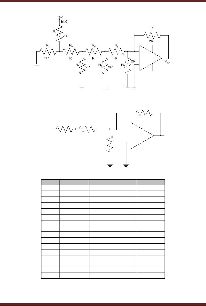
The
R/2R Ladder Digital to
Analogue Converter
The
R/2R D/A Converter derives
its name from the
resistor network having
values R
and
2R. This converter also
overcomes the problem of
having multiple resistors
having
weighted
values. The circuit diagram
of the R/2R converter is
shown. Figure 45.4.
Figure
43.2
R/2R
Ladder D/A Converter
Depending
upon the binary input,
the R/2R resistor network
simplifies to an equivalent
network
which determines the total
current flowing through the
feedback resistance Rf. For
example,
when 0001 binary is applied
the R/2R circuit simplifies
to the circuit shown.
Figure
45.5a.
Simplifying the circuit
further reduces it to the
Thevenin's equivalent circuit.
Figure
43.5b.
The current flowing through
the feedback resistance Rf is defined by the
equation
0.625V
I=
2R
The
output voltage Vout is
represented by the voltage
drop across Rf.
Table 45.3 gives
a summary of
the total current and
the output voltage for
each of the 16 combinations of
4-bit
binary
input.
458
CS302 -
Digital Logic & Design
Figure
45.5a The R/2R resistor
network with binary
0001
Rf
2R
RTh
R8
+0.625V
R
R
Vout
2R
R7
Figure
45.3b The equivalent R/2R
resistor network with binary
0001
Input
Vth (volts)
Current
through Rf
Vout
0000
0
0
0
0001
0.625V
0.625V/2R
-0.625V
0010
1.25V
1.25V/2R
-1.25V
0011
1.875V
1.875V/2R
-1.875V
0100
2.5V
2.5V/2R
-2.5V
0101
3.125V
3.125V/2R
-3.125V
0110
3.75V
3.75V/2R
-3.75V
0111
4.325V
4.325V/2R
-4.325V
1000
5V
5V/2R
-5V
1001
5.625V
5.625V/2R
-5.625V
1010
6.25V
6.25V/2R
-6.25V
1011
6.875V
6.875V/2R
-6.875V
1100
7.5V
7.5V/2R
-7.5V
1101
8.125V
8.125V/2R
-8.125V
1110
8.75V
8.75V/2R
-8.75V
1111
9.325V
9.325V/2R
-9.325V
Table
45.3
D/A
Output voltages for binary
inputs 0000 to 1111
Performance
characteristics of Digital-to-Analogue
Converters
Performance
characteristics of D/A converters
are determined by five
parameters.
459

CS302 -
Digital Logic & Design
1.
Resolution
Resolution is
defined as the number of
bits that are converted. It
is also defined as a
reciprocal of
the number of discrete steps
in the output represented as
percentage. The
resolution of a
4-bit D/A converter is
therefore represented as (1/15)
100 = 6.67%. An 8-bit
D/A
converter
has a resolution of (1/63)
100 = 1.59%.
2.
Accuracy
Accuracy of a
D/A converter is determined by
comparing the actual output
of a D/A
converter
with the expected output. It
is expressed as a percentage of the
full-scale or
maximum
output voltage. If for
example, the accuracy is
±0.1 %, for a D/A converter
which has
a maximum
output of 20 volts, the
maximum error for any
output voltage is (20)(0.001) =
20
mV.
Ideally, the accuracy should
not be worse than ±1/2 of
the least significant bit.
For an 8-bit
D/A
converter, the least
significant bit is 0.39% of
the full-scale. The accuracy
should be one-
half of
0.39%, that is ±0.195%. In
terms of voltage, consider
that the full-scale output
of the 8-
bit
D/A converter is 64 volts.
The maximum error that is
allowed is (64)(0.00195) =
0.1248
volts =
125 mV. Each discrete
step of the D/A converter is
equal to 0.25 volts = 250
mV.
Assuming
that 00000001 is applied at
the input of the D/A
converter, the exact
analogue
output
should be 250 mV. If there
is an error in the output
voltage then the acceptable
range of
voltages
representing 00000001 are
from 125 mV to 375 mV. A
voltage output which is
less
than
125 mV represents the binary
value 00000000 and a voltage
output which exceeds
375
mV represents
the binary value 00000010.
Thus the error should be
within ±1/2% of the
least
significant
bit.
3.
Linearity
The
output of the D/A converter
should be a straight line
when the binary input is
varied
between
its minimum and maximum
values. An offset error is
determined by the output
voltage
when
the binary input bits
are all set to logic
0.
4.
Monotonicity
The
output of the D/A converter
should give an increasing
analogue voltage
output
when
the binary input is varied
between its minimum and
maximum values. However, if
the
D/A
converter outputs a lower
voltage than its preceding
output voltage the converter
is said to
exhibit
non-monotonic behavior.
5. Settling
Time
Ideally,
the D/A converter should
immediately result in an analogue
output
corresponding to
the input binary value. A
D/A converter however takes
a finite amount of
time
to output an
analogue value corresponding to
the binary input. The
settling time of a
D/A
converter is
defined as the time the
D/A converter takes to
settle within ±1/2 least
significant
bit of
its final value when a
change occurs in the input.
Assume that the input to an
8-bit D/A
converter is
00000101 which is represented by
1.250 Volts. The binary
input changes to
00000001
which is represented by 250
mV. The output of the
D/A converter changes
form
1.250
volts to 375 mV (±1/2 least
significant bit of the final
value 250 mV) in 20 msec.
Thus the
settling
time of the D/A converter is
20 msec.
460
Table of Contents:
- AN OVERVIEW & NUMBER SYSTEMS
- Binary to Decimal to Binary conversion, Binary Arithmetic, 1s & 2s complement
- Range of Numbers and Overflow, Floating-Point, Hexadecimal Numbers
- Octal Numbers, Octal to Binary Decimal to Octal Conversion
- LOGIC GATES: AND Gate, OR Gate, NOT Gate, NAND Gate
- AND OR NAND XOR XNOR Gate Implementation and Applications
- DC Supply Voltage, TTL Logic Levels, Noise Margin, Power Dissipation
- Boolean Addition, Multiplication, Commutative Law, Associative Law, Distributive Law, Demorgans Theorems
- Simplification of Boolean Expression, Standard POS form, Minterms and Maxterms
- KARNAUGH MAP, Mapping a non-standard SOP Expression
- Converting between POS and SOP using the K-map
- COMPARATOR: Quine-McCluskey Simplification Method
- ODD-PRIME NUMBER DETECTOR, Combinational Circuit Implementation
- IMPLEMENTATION OF AN ODD-PARITY GENERATOR CIRCUIT
- BCD ADDER: 2-digit BCD Adder, A 4-bit Adder Subtracter Unit
- 16-BIT ALU, MSI 4-bit Comparator, Decoders
- BCD to 7-Segment Decoder, Decimal-to-BCD Encoder
- 2-INPUT 4-BIT MULTIPLEXER, 8, 16-Input Multiplexer, Logic Function Generator
- Applications of Demultiplexer, PROM, PLA, PAL, GAL
- OLMC Combinational Mode, Tri-State Buffers, The GAL16V8, Introduction to ABEL
- OLMC for GAL16V8, Tri-state Buffer and OLMC output pin
- Implementation of Quad MUX, Latches and Flip-Flops
- APPLICATION OF S-R LATCH, Edge-Triggered D Flip-Flop, J-K Flip-flop
- Data Storage using D-flip-flop, Synchronizing Asynchronous inputs using D flip-flop
- Dual Positive-Edge triggered D flip-flop, J-K flip-flop, Master-Slave Flip-Flops
- THE 555 TIMER: Race Conditions, Asynchronous, Ripple Counters
- Down Counter with truncated sequence, 4-bit Synchronous Decade Counter
- Mod-n Synchronous Counter, Cascading Counters, Up-Down Counter
- Integrated Circuit Up Down Decade Counter Design and Applications
- DIGITAL CLOCK: Clocked Synchronous State Machines
- NEXT-STATE TABLE: Flip-flop Transition Table, Karnaugh Maps
- D FLIP-FLOP BASED IMPLEMENTATION
- Moore Machine State Diagram, Mealy Machine State Diagram, Karnaugh Maps
- SHIFT REGISTERS: Serial In/Shift Left,Right/Serial Out Operation
- APPLICATIONS OF SHIFT REGISTERS: Serial-to-Parallel Converter
- Elevator Control System: Elevator State Diagram, State Table, Input and Output Signals, Input Latches
- Traffic Signal Control System: Switching of Traffic Lights, Inputs and Outputs, State Machine
- Traffic Signal Control System: EQUATION DEFINITION
- Memory Organization, Capacity, Density, Signals and Basic Operations, Read, Write, Address, data Signals
- Memory Read, Write Cycle, Synchronous Burst SRAM, Dynamic RAM
- Burst, Distributed Refresh, Types of DRAMs, ROM Read-Only Memory, Mask ROM
- First In-First Out (FIFO) Memory
- LAST IN-FIRST OUT (LIFO) MEMORY
- THE LOGIC BLOCK: Analogue to Digital Conversion, Logic Element, Look-Up Table
- SUCCESSIVE APPROXIMATION ANALOGUE TO DIGITAL CONVERTER