 |
CS302 -
Digital Logic & Design
Lesson
No. 09
BOOLEAN
ALGEBRA AND LOGIC
SIMPLIFICATION
Boolean
Analysis of Logic Circuits,
evaluating of Boolean expressions,
representing
the
operation of Logic circuits
and Boolean expressions in
terms of Function tables
and
representing
Boolean expressions in SOP
and POS forms are
inter-related. Boolean
laws,
rules
and theorems are used to
readily change from one
form of representation to the
other.
Two
examples are considered
which illustrate the
analysis, simplification
and
representation
of Logic Circuits and
Boolean expressions. In both
the examples, a
Boolean
expression
representing the Logic
Circuit is developed, the
Boolean expression is
evaluated
and a
function table is implemented
that represents the Boolean
expression and the
function
of the
Logic Circuit. Each Boolean
expression is also simplified
into SOP or POS form,
the
simplified
expression is presented in a function
table format. The original
and the simplified
expressions
are verified to show
identical functions.
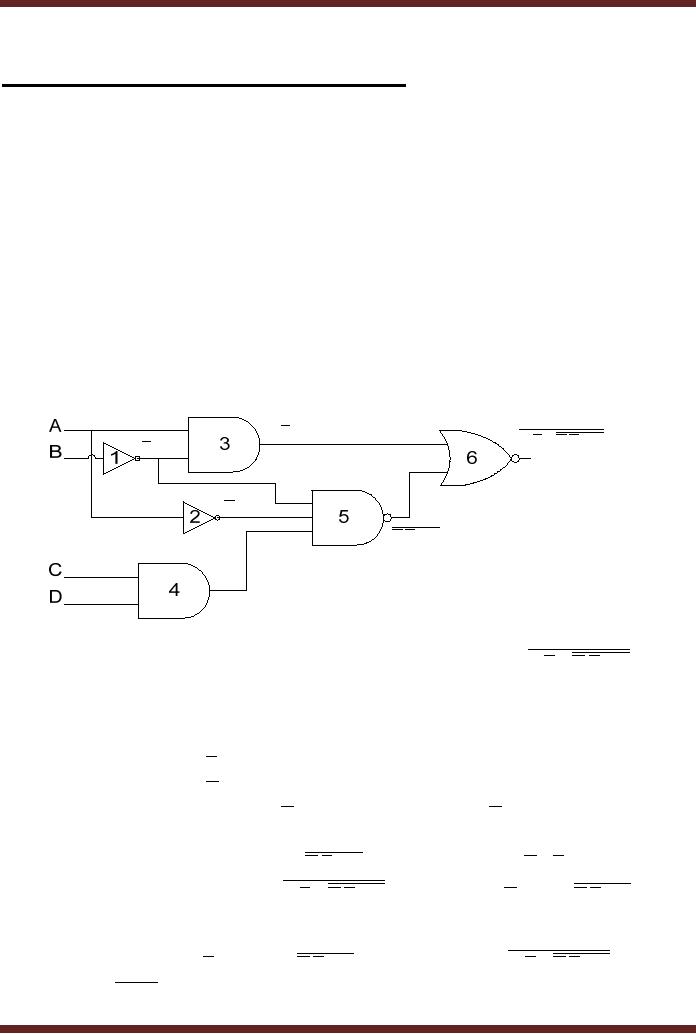
Example
1
1. Finding
the Boolean
Expression
A.B
A.B + A.B.C.D
B
A
A.B.C.D
C.D
Logic
Circuit represented by Boolean
expression A.B + A.B.C.D
Figure
9.1
The
circuit can be represented by a
Boolean Expression. Starting
from the left
hand
side
· Output of
NOT gate 1 is B
· Output of
NOT gate 2 is A
· Output of
two input AND gate 3 is A.B
(product of
A and B
· Output of
two input AND gate 4 is C.D
(product of C
and D)
·
Output of
three input NAND gate 5 is A.B.C.D
NOT(product of
A , B and
CD)
Output of
two input NOR gate 6 is
A.B + A.B.C.D
·
NOT(sum of
A.B and A.B.C.D )
2. Evaluating
the Expression
and Y = A.B.C.D .
expression
A.B + A.B.C.D
X = A.B
The
can
be
Considering
that
represented by
X + Y .
79
CS302 -
Digital Logic & Design
The
output of the logic circuit
is 1 when X = 0 and Y = 0
· X=0
NOR Y=0 Output = 1
· X=0
NOR Y=1 Output = 0
· X=1
NOR Y=0 Output = 0
· X=1
NOR Y=1 Output = 0
X= A.B = 0 when any
literal is zero. That is,
A =0 or B =0
(B=1)
Y= A.B.C.D = 0 when A.B.C.D = 1
A.B.C.D = 1 when all
literals are one. That is
A =1 (A=0), B =1 (B=0), C=1 and
D=1
The
expression output is 1 for
the input conditions
(A=0 OR
B=1) AND (A=0 AND B=0 AND
C=1 AND D=1)
That
is, A=0, B=0, C=1and
D=1.
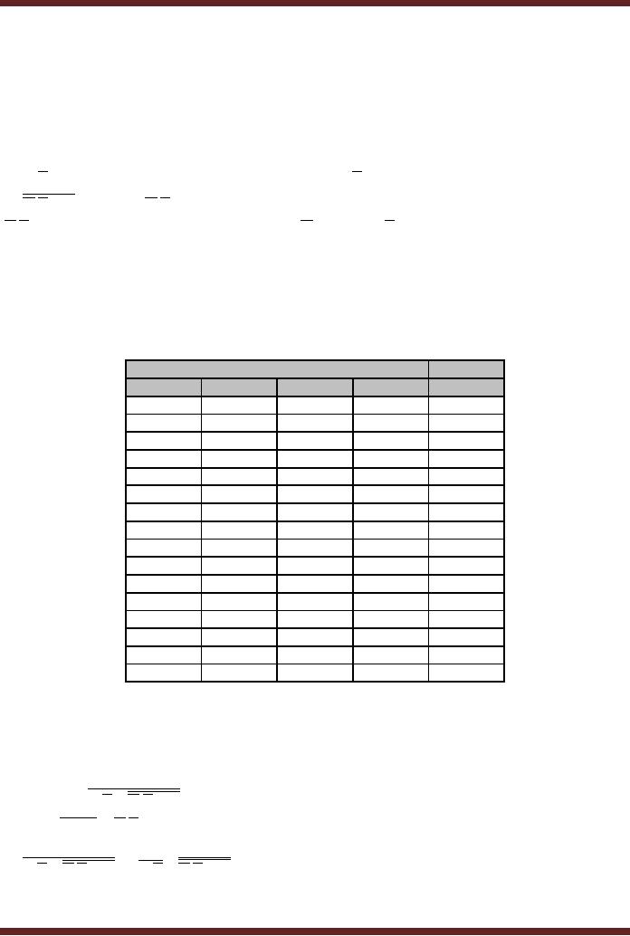
3. Putting
the Results in Truth Table
Format
Input
Output
A
B
C
D
F
0
0
0
0
0
0
0
0
1
0
0
0
1
0
0
1
0
0
1
1
0
1
0
0
0
0
1
0
1
0
0
1
1
0
0
0
1
1
1
0
1
0
0
0
0
1
0
0
1
0
1
0
1
0
0
1
0
1
1
0
1
1
0
0
0
1
1
0
1
0
1
1
1
0
0
1
1
1
1
0
Table
9.1
Truth
Table representing function of
Logic Circuit (fig.
9.1)
4. Simplification
of Boolean Expression
The A.B + A.B.C.D expression can be
simplified by applying Demorgan's
second
theorem
A + B = A.B .
= ( A.B + A.B.C.D = (A.B).(A.B.C.D)
Apply
Demorgan's first theorem to
the first term and
Rule 9 to the second
term
80
CS302 -
Digital Logic & Design
= (A + B).(A.B.C.D)
= (A + B).(A.B.C.D)
Using
the Distributive Law
= (A.A.B.C.D) + A.B.B.C.D
Applying
Rule 8 to the second
term
= A.B.C.D
expression =1
when all literals are
one
that is
A =1 AND B =1 AND
C=1 AND D=1
or A=0 AND
B=0 AND C=1 AND D=1
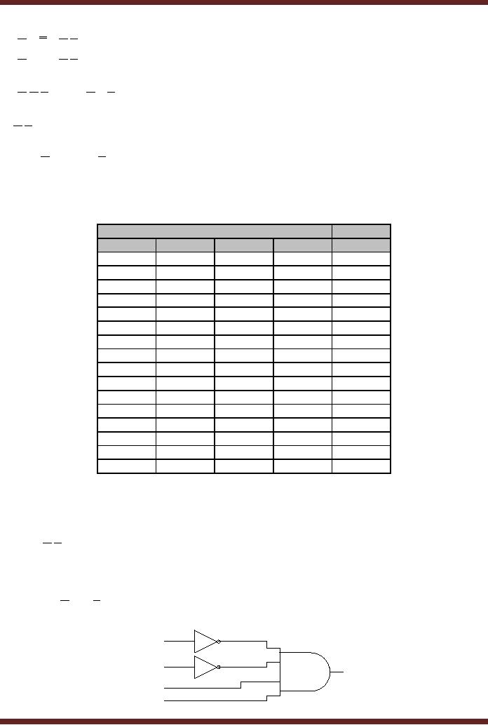
5. Putting
the result in Truth Table
format
Input
Output
A
B
C
D
F
0
0
0
0
0
0
0
0
1
0
0
0
1
0
0
1
0
0
1
1
0
1
0
0
0
0
1
0
1
0
0
1
1
0
0
0
1
1
1
0
1
0
0
0
0
1
0
0
1
0
1
0
1
0
0
1
0
1
1
0
1
1
0
0
0
1
1
0
1
0
1
1
1
0
0
1
1
1
1
0
Table
9.2
Truth
Table representing function of
simplified expression
6. Implementing
Logic Circuit from
Simplified Boolean
expression
F = A.B.C.D
The
expression F represents a product
term having four literals.
Product term is
implemented
using AND
gates. Since, the product
has four literals therefore
a 4-input AND gate is
used.
The
literals A
and B are implemented using
NOT gates.
A
3
B
4
7
C
D
81

CS302 -
Digital Logic & Design
Figure
9.2
Simplified
Logic Circuit
Example
2
1. Finding
the Boolean
Expression
A
A.B.C
(A.B.C).(C + D)
C
C+D
Logic
Circuit represented by Boolean
expression (A.B.C).(C + D)
Figure
9.3
The
circuit can be represented by a
Boolean Expression. Starting
from the left
hand
side
· Output of
NOT gate 1 is A
· Output of
NOT gate 2 is C
·
Output of
three input AND gate 4 is A.B.C
(product of
A , B and C )
Output of
two input OR gate 5 is C + D
·
(sum of
C and D)
Output of NAND
gate 6 is (A.B.C).(C + D)
NOT(product of
A.B.C and C + D )
·
2. Evaluating
the Expression
Considering
that X
=
A.B.C and Y = C + D . The expression
(A.B.C).(C + D) can
be
represented by
X.Y .
The
output of the logic circuit
is 1 when X=0 or Y=0
· X=0 NAND
Y=0 Output = 1
· X=0 NAND
Y=1 Output = 1
· X=1 NAND
Y=0 Output = 1
· X=1 NAND
Y=1 Output = 0
X= A.B.C = 0 when any
literal is zero. That is,
A =0 (A=1) or B =0 or
C =0 (C=1)
Y= C + D = 0 when both
literals are zero. That is
C =0 (C=1) and
D=0
The
expression output is 1 for
the input conditions
(A=1 OR
B=0 OR C=1) OR (C=1 AND
D=0)
82

CS302 -
Digital Logic & Design
3. Putting
the Results in Truth Table
Format
Input
Output
A
B
C
D
F
0
0
0
1
0
0
0
1
1
0
0
1
0
1
0
0
1
1
0
1
0
1
0
0
0
0
1
0
1
0
0
1
1
1
0
0
1
1
1
1
0
0
1
1
0
0
1
1
1
0
1
1
0
1
0
1
1
1
0
1
1
0
0
1
1
1
0
1
1
1
1
1
1
1
0
1
1
1
1
1
Table
9.2
Truth
Table representing function of
Logic Circuit (fig.
9.3)
The
truth table shows that
the variable D has no effect
on the output of the
circuit. The truth
table
reduces to a three variable
truth table. Table
9.3
4. Simplification
of Boolean Expression
The (A.B.C).(C + D) expression
can be simplified by applying
Demorgan's first
theorem
A.B = A + B .
= (A.B.C).(C + D) = (A.B.C) + (C + D)
Input
Output
A
B
C
F
0
0
0
1
0
0
1
1
0
1
0
0
0
1
1
1
1
0
0
1
1
0
1
1
1
1
0
1
1
1
1
1
Table
9.3
Alternate
Truth Table representing
function of Logic Circuit
(fig. 9.3)
Apply
Demorgan's first and second
theorems to the first and
second terms
respectively
83
CS302 -
Digital Logic & Design
= (A + B + C) + (C.D)
Applying
Rule 9
= (A + B + C) + (C.D)
= A + B + C(1 + D)
= A +B+C
expression =1
when any one literal is
one
that is
A=1 OR B
=1 OR
C=1
or A=1 OR
B=0 OR C=1
5. Putting
the result in Truth Table
format
Input
Output
A
B
C
F
0
0
1
0
0
1
0
1
0
1
0
0
0
1
1
1
0
1
1
0
1
1
0
1
1
0
1
1
1
1
1
1
Table
9.4
Truth
Table representing function of
simplified expression
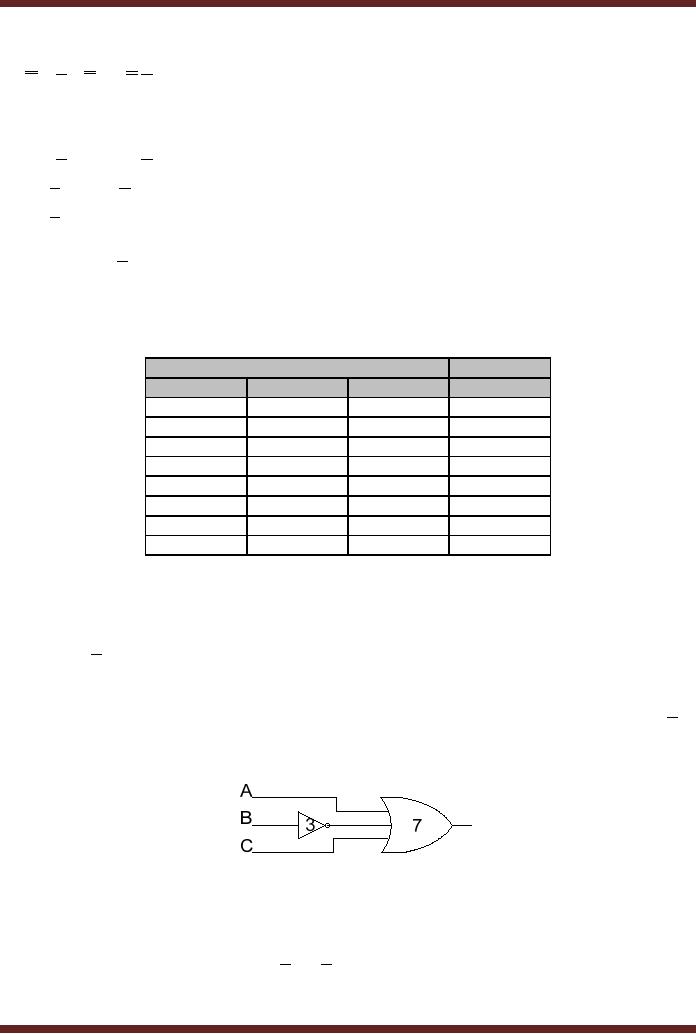
6. Implementing
Logic Circuit from
Simplified Boolean
expression
F = A +B+C
The
expression F represents a sum
term having three literals.
Sum term is implemented
using
OR gates.
Since, the sum has
three literals therefore a
3-input OR gate is used. The
literal B
is
implemented
using NOT gate.
Figure
9.4
Simplified
Logic Circuit
Standard
SOP form
A standard
SOP form has product
terms that have all
the variables in the domain
of the
expression.
The SOP expression AC + BC is not a
standard SOP as the domain
of the
expression
has variables A, B and
C.
84

CS302 -
Digital Logic & Design
A non-standard
SOP is converted into a
standard SOP by using the
rule A + A = 1
AC + BC
= AC(B + B) + (A + A)BC
= ABC + ABC + ABC + ABC
= ABC + ABC + ABC
Standard
POS form
A standard
POS form has sum
terms that have all
the variables in the domain
of the
expression.
The POS expression (A + B + C)(A + B + D)(A + B + C + D) is not a
standard
POS as
the domain of the expression
has variables A, B, C and
D.
A non-standard
POS is converted into a
standard POS by using the
rule AA = 0
(A + B + C)(A + B + D)(A + B + C + D)
= (A + B + C + D)(A + B + C + D)(A + B + C + D)(A + B + C + D)(A + B + C + D)
Converting to
Standard SOP and POS
forms
There
are several reasons for
converting SOP and POS
forms into standard SOP
and
POS
forms respectively.
Any logic
circuit can be implemented by
using either the SOP,
AND-OR combination of
gates or
POS, OR-AND combination of
gates. It is very simple to
convert from standard
SOP
to standard
POS or vice versa. This
helps in selecting an implementation
that requires the
minimum
number of gates. Secondly,
the simplification of general
Boolean expression by
applying
the laws, rules and
theorems does not always
result in the simplest form
as the ability
to apply
all the rules depends on
ones experience and
knowledge of all the
rules.
A simpler
mapping method uses Karnaugh
maps to simplify general
expressions.
Mapping of
all the terms in a SOP
form expression and the
sum terms in a POS form
can be
easily
done if standard forms of
SOP and POS expressions
are used. Karnaugh maps
will be
discussed
latter in the
chapter.
Lastly,
the PLDs are implemented
having a general purpose
structure based on
AND-
OR arrays. A
function represented by an expression in
Standard SOP form can be
readily
programmed.
Minterms
and Maxterms
The
Product terms in the
Standard SOP form are
known as Minterms and the
Sum
terms in
the Standard POS form
are known as
Maxterms.
A
B
C
Minterms
Maxterms
A +B+C
0
0
0
A.B.C
0
0
1
A +B+C
A.B.C
0
1
0
A +B+C
A.B.C
85

CS302 -
Digital Logic & Design
0
1
1
A +B+C
A.B.C
1
0
0
A +B+C
A.B.C
1
0
1
A +B+C
A.B.C
1
1
0
A +B+C
A.B.C
A.B.C
1
1
1
A +B+C
Table
9.5
Table of
Minterms and Maxterms
Binary
representation of a standard Product
term or Minterm
A standard
product term is equal to one
for only one combination of
variable values.
For
all other variable values
the standard product term is
equal to zero.
For
the expression ABC + ABC + ABC
ABC =1
if A=1,
B=1 and C=0
ABC =1
if A=1,
B=0 and C=0
ABC =1
if A=0,
B=1 and C=0
An SOP
expression is equal to 1 when
one or more product terms in
the expression are
equal
to 1.
Binary
representation of a standard Sum term or
Maxterm
A standard
sum term is equal to zero
for only one combination of
variable values. For
all
other variable values the
standard sum term is equal
to one.
For
the expression
(A + B + C + D)(A + B + C + D)(A + B + C + D)(A + B + C + D)(A + B + C + D)
(A + B + C + D) =0
if A=0,
B=1, C=0 and
D=1
(A + B + C + D) =0
if A=0,
B=1, C=0 and
D=0
(A + B + C + D) =0
if A=0,
B=0, C=1 and
D=1
(A + B + C + D) =0
if A=0,
B=0, C=0 and
D=1
(A + B + C + D) =0
if A=0,
B=1, C=1 and
D=0
A POS
expression is equal to 0 when
one or more product terms in
the expression are
equal
to 0.
Converting
Standard SOP into Standard
POS
The
binary values of the product
terms in a given standard
SOP expression are
not
present in
the equivalent standard POS
expression. Also, the binary
values that are
not
represented in
the SOP expression are
present in the equivalent
POS expression.
ABC + ABC + ABC + ABC + ABC
has
the binary values 000,
010,011,101 and 111
Canonical
Sum = ∑ A,B,C (0,2,3,5,7) = ABC + ABC + ABC + ABC + ABC
The
missing binary values are
001, 100 and
110.
The
POS expression is (A + B + C)(A + B + C)(A + B + C)
86

CS302 -
Digital Logic & Design
Canonical
Product = ∏ A,B,C (1,4,6)
Verifying
POS expression is equivalent to
SOP expression
(A + B + C)(A + B + C)(A + B + C)
= (A.A + A.B + A.C + A.B + B.B + B.C + A.C + B.C + C.C).(A + B + C)
= (A.B + A.C + A.B + B + B.C + A.C + B.C).(A + B + C)
= (A.C + B + A.C).(A + B + C)
= A.A.C + A.B.C + A.C.C + A.B + B.B + B.C + A.A.C + A.B.C + A.C.C
= A.B.C + A.C + A.B + B.C + A.C + A.B.C
Converting
into standard SOP
= A.B.C + A.C(B + B) + A.B(C + C) + B.C(A + A) + A.C(B + B) + A.B.C
= A.B.C + A.B.C + A.B.C + A.B.C + A.B.C + A.B.C + A.B.C + A.B.C + A.B.C + A.B.C
Simplifies
to
= ABC + ABC + ABC + ABC + ABC
Therefore
∑(0,2,3,5,7) = ∏(1,4,6)
Boolean
Expressions and Truth
Tables
All
standard Boolean expressions
can be easily converted into
truth table format
using
binary
values for each term in
the expression. Standard SOP
or POS expressions can also
be
determined
from a truth table.
Converting
SOP expression to Truth
Table format
A truth
table is a list of possible
input variable combinations
and their
corresponding
output
values. An SOP expression
having a domain of 2 variables
will have a truth
table
having 4
combinations of inputs and
corresponding output
values.
To convert an
SOP expression in a Truth
table format, a truth table
having input
combinations
proportional to the domain of
variables in the SOP
expression is written.
Next
the
SOP expression is written in a
standard SOP form. In the
last step all the
sum terms
present in
the standard SOP expression
are marked as 1 in the
output.
AB + BC has a
domain of three variables
thus a truth table having 8
input and output
combinations is
required. The SOP expression
is converted into standard
SOP expression
AB(C + C) + BC(A + A) = ABC + ABC + ABC
+
ABC
=
ABC
+
ABC
+
ABC
+
ABC
Marking
the outputs in the truth
table as 1 for sum terms
that are present in the
standard SOP.
Input
Output
A
B
C
F
0
0
0
0
0
0
1
0
0
1
0
0
0
1
1
1
1
0
0
1
1
0
1
1
87
CS302 -
Digital Logic & Design
1
1
0
0
1
1
1
1
Table
9.6
Mapping
SOP expression to Truth
Table
Canonical
Sum F= ∑ A,B,C (3,4,5,7) = A.B.C + A.B.C + A.B.C + A.B.C
Converting
POS expression to Truth
Table format
An POS
expression having a domain of 2
variables will have a truth
table having 4
combinations of
inputs and corresponding
output values. To convert a
POS expression in a
Truth
table format, a truth table
having input combinations
proportional to the domain
of
variables in
the POS expression is
written. Next the POS
expression is written in a
standard
POS
form. In the last step
all the product terms
present in the standard POS
expression are
marked as 0 in
the output.
(A + B)(B + C) has a
domain of three variables
thus a truth table having 8
input and
output
combinations is required. The
POS expression is converted
into standard POS
expression
(A + B + CC)(AA + B + C) = (A + B + C)(A + B + C)(A + B + C)(A + B + C)
Marking
the outputs in the truth
table as 0 for product terms
that are present in the
standard
POS
Input
Output
A
B
C
F
0
0
0
1
0
0
1
0
0
1
0
0
0
1
1
0
1
0
0
1
1
0
1
0
1
1
0
1
1
1
1
1
Table
9.7
Mapping
POS expression to Truth
Table
Canonical
Product F= ∏ A,B,C (1,2,3,5) = (A + B + C)(A + B + C)(A + B + C)(A + B + C)
88
Table of Contents:
- AN OVERVIEW & NUMBER SYSTEMS
- Binary to Decimal to Binary conversion, Binary Arithmetic, 1s & 2s complement
- Range of Numbers and Overflow, Floating-Point, Hexadecimal Numbers
- Octal Numbers, Octal to Binary Decimal to Octal Conversion
- LOGIC GATES: AND Gate, OR Gate, NOT Gate, NAND Gate
- AND OR NAND XOR XNOR Gate Implementation and Applications
- DC Supply Voltage, TTL Logic Levels, Noise Margin, Power Dissipation
- Boolean Addition, Multiplication, Commutative Law, Associative Law, Distributive Law, Demorgans Theorems
- Simplification of Boolean Expression, Standard POS form, Minterms and Maxterms
- KARNAUGH MAP, Mapping a non-standard SOP Expression
- Converting between POS and SOP using the K-map
- COMPARATOR: Quine-McCluskey Simplification Method
- ODD-PRIME NUMBER DETECTOR, Combinational Circuit Implementation
- IMPLEMENTATION OF AN ODD-PARITY GENERATOR CIRCUIT
- BCD ADDER: 2-digit BCD Adder, A 4-bit Adder Subtracter Unit
- 16-BIT ALU, MSI 4-bit Comparator, Decoders
- BCD to 7-Segment Decoder, Decimal-to-BCD Encoder
- 2-INPUT 4-BIT MULTIPLEXER, 8, 16-Input Multiplexer, Logic Function Generator
- Applications of Demultiplexer, PROM, PLA, PAL, GAL
- OLMC Combinational Mode, Tri-State Buffers, The GAL16V8, Introduction to ABEL
- OLMC for GAL16V8, Tri-state Buffer and OLMC output pin
- Implementation of Quad MUX, Latches and Flip-Flops
- APPLICATION OF S-R LATCH, Edge-Triggered D Flip-Flop, J-K Flip-flop
- Data Storage using D-flip-flop, Synchronizing Asynchronous inputs using D flip-flop
- Dual Positive-Edge triggered D flip-flop, J-K flip-flop, Master-Slave Flip-Flops
- THE 555 TIMER: Race Conditions, Asynchronous, Ripple Counters
- Down Counter with truncated sequence, 4-bit Synchronous Decade Counter
- Mod-n Synchronous Counter, Cascading Counters, Up-Down Counter
- Integrated Circuit Up Down Decade Counter Design and Applications
- DIGITAL CLOCK: Clocked Synchronous State Machines
- NEXT-STATE TABLE: Flip-flop Transition Table, Karnaugh Maps
- D FLIP-FLOP BASED IMPLEMENTATION
- Moore Machine State Diagram, Mealy Machine State Diagram, Karnaugh Maps
- SHIFT REGISTERS: Serial In/Shift Left,Right/Serial Out Operation
- APPLICATIONS OF SHIFT REGISTERS: Serial-to-Parallel Converter
- Elevator Control System: Elevator State Diagram, State Table, Input and Output Signals, Input Latches
- Traffic Signal Control System: Switching of Traffic Lights, Inputs and Outputs, State Machine
- Traffic Signal Control System: EQUATION DEFINITION
- Memory Organization, Capacity, Density, Signals and Basic Operations, Read, Write, Address, data Signals
- Memory Read, Write Cycle, Synchronous Burst SRAM, Dynamic RAM
- Burst, Distributed Refresh, Types of DRAMs, ROM Read-Only Memory, Mask ROM
- First In-First Out (FIFO) Memory
- LAST IN-FIRST OUT (LIFO) MEMORY
- THE LOGIC BLOCK: Analogue to Digital Conversion, Logic Element, Look-Up Table
- SUCCESSIVE APPROXIMATION ANALOGUE TO DIGITAL CONVERTER