 |
OLMC Combinational Mode, Tri-State Buffers, The GAL16V8, Introduction to ABEL |
| << Applications of Demultiplexer, PROM, PLA, PAL, GAL |
| OLMC for GAL16V8, Tri-state Buffer and OLMC output pin >> |
CS302 -
Digital Logic & Design
Lesson
No. 20
IMPLEMENTING
CONSTANT 0S AND 1S
The
PLA can be programmed to
give an output of constant 0 or 1.
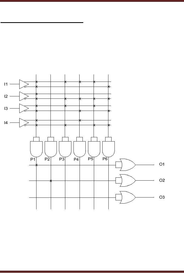
Figure 20.1. All
the
four
inputs and their complements
are shown connected to the
first AND gate. The
product
term
generated by the AND gate is 0.
P1 = 0 . The P1
product term is connected to
the input of
first OR
gate. Thus the output of OR
gate is 0. The inputs to the
second AND gate are
disconnected,
thus the product term
generated by the AND gate is a 1.
P2 = 1 . The P2
term is
connected to
the input of the second OR
gate, therefore the output
of the second OR gate is
a
1. No product
term is connected to the
input of the third OR gate,
therefore the output of
the
third OR
gate is 0.
Figure
20.1
4 x 3 PLA
Device programmed for 0, 1
and 0 output
Implementing
Odd-Prime Number
Function
The
Odd-Prime Number generator
can be implemented by programming
the 4 x 3 PLA.
Due to
the limitations of the PLA
which only has six
product term (six AND
gates), only the
first
six
Odd-Prime numbers 1, 3, 5, 7, 11 and 13
can be detected. Additional
two outputs are
programmed to
detect Odd-Prime multiples of 15
and 39 respectively. The six
product terms
represented by
P1, P2, P3, P4, P5
and P6 are minterms 1, 3, 5, 7, 11
and 13. The first
OR
gate
sums the six minterms
(product terms) to give an
output of 1 when any one of
the first six
Odd-Prime
numbers is applied at the
inputs I1, I2, I3 and I4 of
the PLA respectively.
The
second OR
gate sums the minterms 1, 3
and 5. Thus the output of
the second OR gate is a
1
190
CS302 -
Digital Logic & Design
when
any of the three minterms is
applied at the PLA inputs.
Similarly, the third OR gate
sums
the
minterms 1, 3 and 13 and the
output is set to logic 1
when any one of the
three inputs are
detected at
the input of the PLA.
Figure 20.2.
Figure
20.2
4 x 3 PLA
Device programmed to Detect
Odd-Prime Numbers
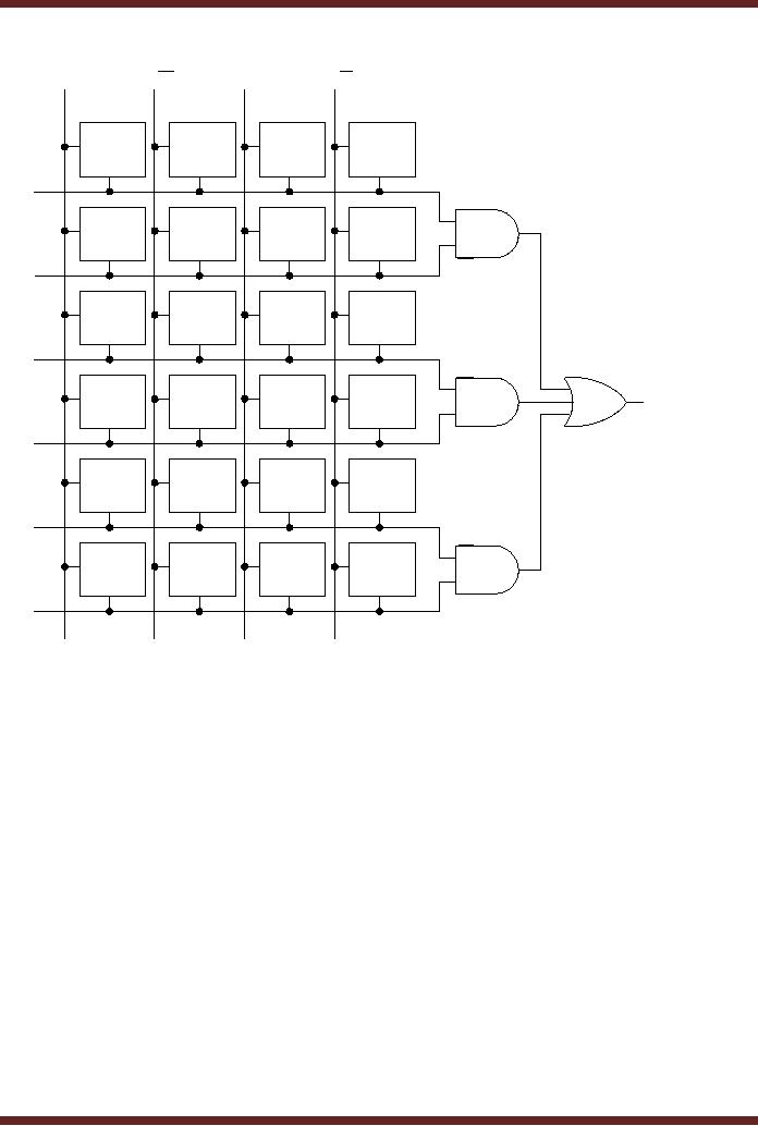
GAL
Operation
The GAL
has a reprogrammable AND gate
array and a fixed OR array.
GAL can be
reprogrammed as
instead of fuses E2CMOS
logic is used which can be
programmed to
connect a
column with a row. The
E2CMOS logic at
each columnrow intersection is
known as
a cell.
Figure 20.3. The E2CMOS cell in the
`on' state connects the
column with the row
and a
cell in
the `off' state disconnects
the column and row.
Appropriate cells are
programmed to the
`on'
state to allow appropriate
literals to be connected to the AND
gates which generate
product
terms. The simplified GAL
structure shows the
implementation of an SOP
function.
Figure
20.4
191
CS302 -
Digital Logic & Design
B
A
A
B
E2CMOS
E2CMOS
E2CMOS
E2CMOS
E2CMOS
E2CMOS
E2CMOS
E2CMOS
E2CMOS
E2CMOS
E2CMOS
E2CMOS
E2CMOS
E2CMOS
E2CMOS
E2CMOS
X
E2CMOS
E2CMOS
E2CMOS
E2CMOS
E2CMOS
E2CMOS
E2CMOS
E2CMOS
Simplified
E2CMOS array
structure of GAL
Figure
20.3
A typical
Gal has eight or more
inputs to the reprogrammable AND
array and 8 or more
input/outputs
from its `Output Logic
Macro Cells' OLMCs. The
OLMCs can be programmed
to
Combinational
Logic or Registered Logic.
Combinational Logic is used
for combinational
circuits,
where as Registered Logic is
based on Sequential circuits.
Figure 20.5
192
CS302 -
Digital Logic & Design
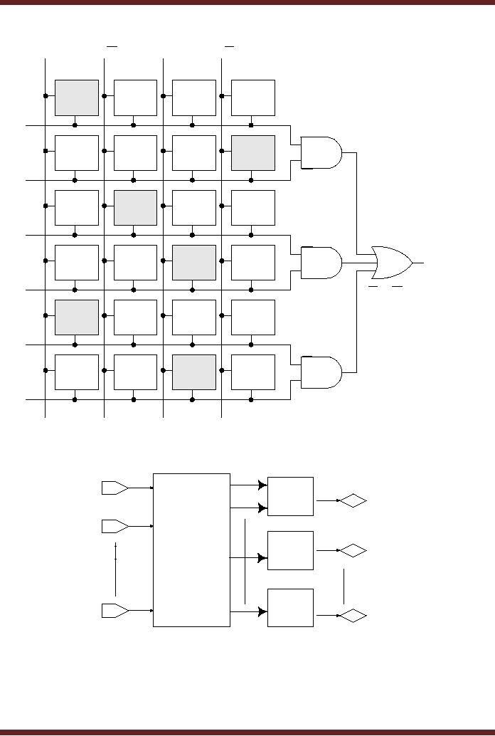
B
A
A
B
ON
OFF
OFF
OFF
OFF
OFF
OFF
ON
OFF
ON
OFF
OFF
OFF
OFF
ON
OFF
AB + AB + AB
ON
OFF
OFF
OFF
OFF
OFF
ON
OFF
Figure
20.4
GAL
implementation of an SOP
function
Input
1
Input/
OLMC
Output
1
Input
2
E2CMOS
Input/
Programmable
OLMC
AND
array
Output
2
Input/
Input
n
OLMC
Output
m
Figure
20.5
Block
diagram of a GAL
193

CS302 -
Digital Logic & Design
GALs
are also available in a
variety of configurations. GALs
are identified by a
prefix
GAL followed by
a 2-digt number indicating
the number of inputs which
is followed by V
indicating
variable output configuration
followed by a number which
indicates the number
of
outputs.
Figure 20.6
G A L 16 V
8
Generic
array Logic
Eight
Outputs
Variable
output Configuration
Sixteen
Inputs
Figure
20.6
Standard GAL
Numbering
Programming of
PLDs
PLDs
are programmed with the
help of computer which runs
the programming
software.
The computer is connected to a
programmer socket in which
the PLD is inserted
for
programming.
PLDs can also be programmed
when they are installed on a
circuit board.
The
programming of a PLD device
involves entering the logic
function in the form of
a
Boolean
equation, truth table or a
state diagram. Any errors
during the entry process
are
corrected.
The software compiler
processes the information in
the input file and
translates it
into a
suitable format. The
complier also minimizes the
logic. The minimized logic
is then
tested by
using a set of hypothetical
inputs known as test
vectors. The testing
verifies the
design of
the logic circuit before
committing it to the PLD. If
any flaws are detected
during the
testing
process the design must be
debugged and submitted for
recompilation. Once
the
design
has been finalized a
documentation file is produced
along with a fuse map
file which is
downloaded to
the programmer which
programs the PLD device
inserted in the
programmer
socket.
PLDs
have In-System Programming
(ISP) capability that allows
the PLDs to be
programmed
after they have been
installed on a circuit board. A
standard 4-wire interface
is
used
for programming the
In-System PLD. ISP
capability allows systems to be
upgraded by
reprogramming
the PLD.
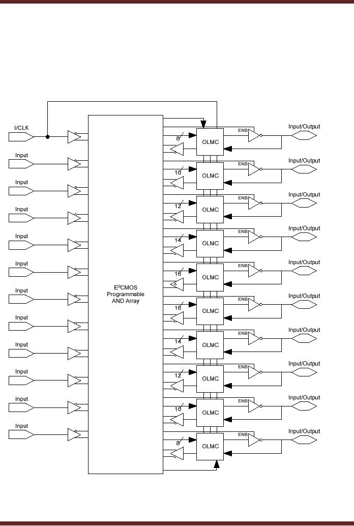
The
GAL22V10
The
GAL22V10 is a popular GAL device
having twelve inputs and
ten inputs/outputs.
The
device is available as low-voltage
3.3v version. It is also
available as an ISP version.
The
device
has ten OLMCs that
can be programmed to different
output modes. The ten
OLMCs
receive
different number of inputs
from the programmable AND
gate array. Figure 20.7. Of
the
ten
OLMCs, two have eight
inputs, two have ten
inputs, two have twelve
inputs, two have
fourteen
and two have sixteen
inputs. Each OLMC can be
programmed for active-high,
active-
low
output or it can be programmed as an
input.
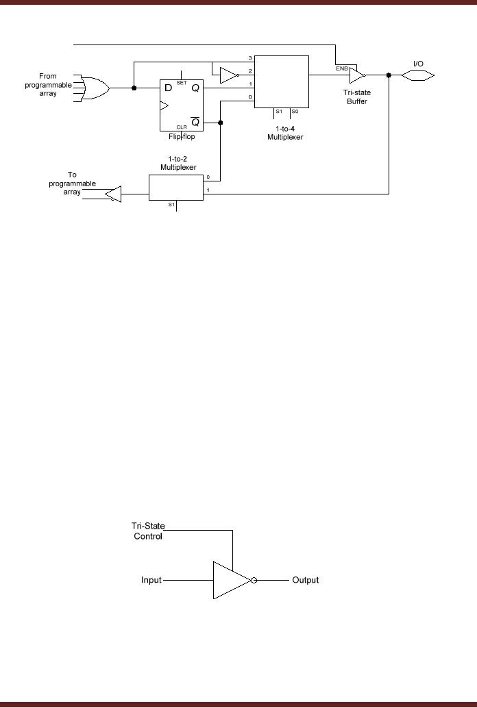
The
circuit diagram of an OLMC is
shown in figure 20.8. The
OLMC consists of a
flip-
flop
which is a sequential logic
device which stores the
information at the output of
the OR
gate.
Flip-flops will be discussed
latter. The output and
the complemented output of
the flip-
flop
are connected to the two
inputs of the 4-to-1 MUX.
The remaining two inputs of
the MUX
are
connected to the OR gate
output and its complemented
output. The output of the
MUX is
connected to
the output through a
tri-state buffer. The output
is also connected to the
input of
194
CS302 -
Digital Logic & Design
a 2-to-1 MUX.
The other input of the
2-to-1 MUX is connected to the
complemented output of
the
flip-flop. The output of the
2-to-1 MUX and its
complemented output is connected to
the
input of
the AND array. The select
inputs S0
and S1 select the appropriate
4-to-1 MUX input to
be routed to
the output or the input.
The S1 select input of
the 2-to-1 MUX is used to
route the
appropriate
input to the input of the
AND array. The select bits
S0 and S1 are programmed in a
dedicated
group of cells in the array
which are separate from
the logic array
cells.
Figure
20.7
Block
diagram of the
GAL22V10
195
CS302 -
Digital Logic & Design
Figure
20.8
Circuit
Diagram of OLMC
The
four OLMC configurations
are
· Combination
Mode with active-low
output
· Combinational
Mode with active-high
output
· Registered
Mode with active-low
output
· Registered
Mode with active-high
output
OLMC
Combinational Mode
When
the select inputs S0 and S1
are
set to 0 and 1 respectively,
the 4-to-1 MUX
selects
the OR gate output and
the output is active-low
because of the inversion by
the tri-
state
buffer. When the select
inputs are set to 1 and 1
respectively, the MUX selects
the
complement of
the OR gate output. The
output of the OLMC is
active-high due to
double
inversion.
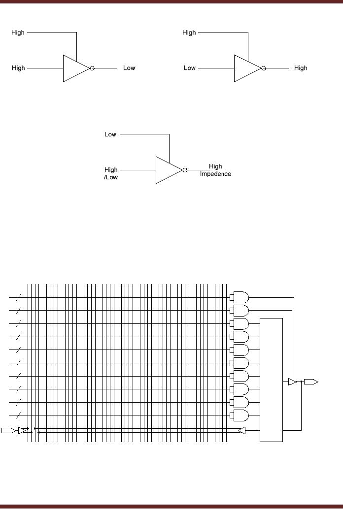
Tri-State
Buffers
Tri-State
Buffer is a NOT gate with a
control line that
disconnects the output from
the
input.
When the control line is
high the buffer operates
like a NOT gate and
when the control
line is
low the output is
disconnected from the output
and high impedance is seen
at the
output.
Tri-state buffers are used
to disconnect the outputs of
devices which are connected
or
share a
common output line. Figure
20.9
Figure
20.9a
Tri-State
Buffer
196
CS302 -
Digital Logic & Design
Figure
20.9b Tri-State Buffer
operating as a NOT
gate
Figure
20.9c Tri-State Buffer in
High-Impedence State
Referring to
the OLMC logic circuit.
Figure 20.8. When the
control input to the
tri-state
buffer is
set to low, the output of
the buffer is set to high
impedance disconnecting the
OLMC
from
the output pin. The
output pin is used as an
input pin.
The
GAL22V10 Array
Input
Lines
Reset to
all OLMCs
44
44
44
44
44
44
Input/Output
OLMC
44
Product
Term Lines
44
44
44
Input
Figure
20.10
Detailed
Connection to the first OLMC
of GAL22V10
The
GAL22V10 has 22 inputs
organized as 44 lines, one
for each input and
its
complement.
Each AND gate has 44 inputs
connected to the 44 input
lines. Detailed
197
CS302 -
Digital Logic & Design
connection of
the first OLMC to the AND
array is shown in figure
20.8. The vertical lines
in
groups of
four represent the inputs.
Thus the first group of
four vertical lines
represents the
input
from the GAL input pin
and the input from
the OLMC. The horizontal
lines represent the
product
terms. The first OLMC
has ten input product
terms. Out of the ten
product terms, eight
product
terms are connected to the
OR gate in the first OLMC.
Out of the remaining
two
product
terms, the first product
term is used to control the
tri-state buffer and the
other is used
for
reset in the Registered mode
for all OLMCs.
Each
OLMC ORs the product
term to give a single sum of
product term. The GAL
has
ten
such OLMCs therefore a total
of ten Sum-of-Product terms
can be implemented.
Programming
the GAL22V10
Figure
20.11 shown the programmed
GAL for the Boolean
expression
X = ABCDEF
+
ABCDEF
+
ABCDEF
+
ABCDEF
+
ABCDEF
+
ABCDEF
+
ABCDEF
Input
Lines
Reset to
all OLMCs
44
x
44
x
x
x
x
x
x
44
x
x
x
x
x
x
44
x
x
x
x
x
x
44
x
x
x
x
x
x
44
x
x
x
x
x
x
Input/Output
OLMC
44
Product
Term Lines
x
x
x
x
x
x
44
x
x
x
x
x
x
44
44
Input
Figure
20.11
GAL22V10
programmed for Boolean
Function
In the
figure 20.9 the GAL has
been programmed for a six
variable Boolean
function.
The
six variables are connected
at the six inputs of the GA
device. The figure shows
the
connection
detail for the first
variable A. The first group
of four vertical lines
represents the
variable A
and its complement A . The remaining two
lines in the group are
not used receive
the
un-complemented and complemented
output from the OLMC.
Similarly, the second
group
of four
vertical lines are connected
to the second input pin of
the GAL which is connected to
a
signal
representing variable B. The
next four sets of four
vertical lines represent
input pins 3,
4, 5 and 6
which are connected to
variables C, D, E and F. The
Boolean expression that
is
implemented
has seven product terms.
The first OLMC has
eight input product terms,
thus it
can be
used to program the Boolean
expression. The output of
the first AND gate
generates
the
first product term of the
Boolean expression. Similarly,
the 2nd
to 7th AND gates generate
the
remaining six product terms
respectively. The eight
input OR gate (not shown) in
the
OLMC
block generates the sum of
product terms. The last
group of vertical lines is
used to
control
the tri-state buffer
connected at the output of
the OLMC. The diagram
shows that it has
198
CS302 -
Digital Logic & Design
been
set to high to allow the
tri-state buffer connect the
OLMC output to the output
pin of the
GAL.
The
GAL16V8
This
device has eight inputs
and eight inputs/output. The
GAL16V8 is designed to be
programmed in
one of the three available
modes to emulate most of the
existing PALs, thus
replacing
the PAL. The three
modes in which PALs are
programmed are
· Simple
· Complex
· Registered
The
simple and complex modes
are associated with the
Combinational Logic whereas
the
Registered
mode is associated with
Sequential Logic.
Simple
Mode
In the
Simple Mode the OLMC is
configured as dedicated active
combinational outputs
or as dedicated
inputs (limited to six).
Three possible combinations of
the Simple Mode are
· Combinational
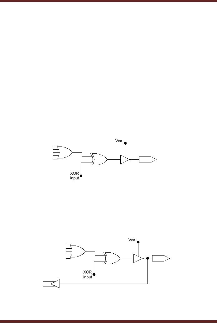
Output. Figure 20.12a
· Combinational
Output with feedback to AND
Array. Fig 20.12b
· Dedicated
input. Fig 20.12c
Figure
20.12a Combinational
Output
In the
Combinational Output the
OLMC is configured to give an
output which is either
active-
low or
active-high. The active-state of
the output is determined by
the XOR input. The
tri-state
buffer
control pin is set to logic
high. The Combinational
Output with feedback to AND
array is
similar.
The tri-state control pin is
set to logic high, the
XOR gate input determines
the active-
state of
the output. The signal at
the output is also connected
to the input of the AND
array
through
the buffer which provides
inverting and non-inverting
outputs.
Figure
20.12b Combinational Output
with feedback to AND
array
199
CS302 -
Digital Logic & Design
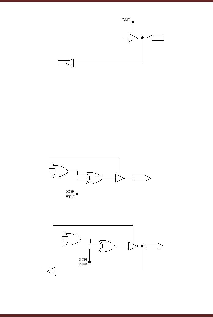
Figure
20.12c Dedicated
Input
In the
Dedicated Input configuration
the tri-state buffer is
configured in the
high
impedance
state by setting the control
pin of the tri-state buffer
to low. Thus the output
pin is
connected t an
input signal which is passed
to the input of the AND
Array in its
complemented
and
un-complemented form by the
buffer.
Complex
Mode
In this
mode the OLMCs can be
configured in two ways. In
the complex Mode the
tri-
state
control is formed by a logical
expression, this leaves
seven product terms that
can be
used to
form a sum-of product
expression.
· Combinational
Output. Fig. 20.13
· Combinational
Input/Output. Fig.
20.14
Figure
20.13
Combinational
Output
Figure
20.14
Combinational
Input/Output
Introduction to
ABEL
ABEL
which is an acronym for
Advanced Boolean Expression
Language is a hardware
description
language used for
implementing logic designs
using PLDs. ABEL is a
device-
200
CS302 -
Digital Logic & Design
independent
language and can be used to
program any type of PLD.
ABEL is run on a
computer
connected to a PLD programmer
which programs the
PLD.
ABEL
provides three different
text-based methods for
describing and entering a
logic
design.
The three methods
are
· Boolean
Equations
· Truth
Tables
· State
Diagrams
The
Boolean Equations and the
Truth Table method are
used for Combinational Logic
Circuits.
The
State Diagram is used
specifically for Sequential
Logic circuits. The Boolean
Equations
and
the Truth Table method
can also be used for
describing and entering
Sequential Logic
Circuits.
Boolean
Operations
The
NOT, AND, OR and XOR
operations have special
symbols in ABEL as shown
in
table
20.1
Logic
Operation
ABEL
Symbol
NOT
!
AND
&
OR
#
XOR
$
Table
20.1
ABEL
Symbols for logic
operations
The
standard Boolean notations in
terms of ABEL notations are
defined in table 20.2
Boolean
Notation
ABEL
Notation
!A
A
A.B
A&B
A +B
A#B
A ⊕B
A$B
Table
20.2
Boolean
and equivalent ABEL
Notations
1. Boolean
Equations
One of
the ABEL entry methods
uses logic equations. In
ABEL any letter or
combination of
letters and numbers can be
used to identify variables.
ABEL however is case-
sensitive,
thus variable `A' is treated
separately from variable
`a'. All ABEL equations
must end
with
`;'. Figure 20.15.
Boolean
expression F
=
AB + AC + BD is written in
ABEL as
F = A & !B # A & C #
!B & !D;
Figure
20.15 ABEL representation of
Boolean expression
201
CS302 -
Digital Logic & Design
The
operators !, &, # and $ have
precedence in the order
given in table 20.1
Multiple
Inputs and
Outputs
In some
cases, multiple input and
output variables can be
grouped as a set to
simplify
an equation.
Fig 20.16. Thus D0, D1 and D2 input or output variables
can be defined by a
single
variable D
using the ABEL notation D =
[D0, D1, D2];
Consider
the ABEL description of a
4-input 4-bit Multiplexer.
Figure 20.1, Table
20.3
Select
Inputs
Outputs
S1
S0
Y3
Y2
Y1
Y0
0
0
A3
A2
A1
A0
0
1
B3
B2
B1
B0
1
0
C3
C2
C1
C0
1
1
D3
D2
D1
D0
Table
20.3
Truth
Table of 4-input 4-bit
MUX
The
Boolean expressions representing
the operation of the MUX
are
Y3 = A 3 S1 S 0 + B3 S1S 0 + C3S1 S 0 + D3S1S 0
Y2 = A 2 S1 S 0 + B 2 S1S 0 + C 2S1 S 0 + D 2S1S 0
Y1 = A 1 S1 S 0 + B1 S1S 0 + C1S1 S 0 + D1S1S 0
Y0 = A 0 S1 S 0 + B 0 S1S 0 + C 0S1 S 0 + D 0S1S 0
The
ABEL notations representing
the operation of the MUX
are
Y3 = A3 &
!S1 & !S0 # B3 & !S1 & S0 #
C3 & S1 & !S0 # D3 & S1 &
S0;
Y2 = A2 &
!S1 & !S0 # B2 & !S1 & S0 #
C2 & S1 & !S0 # D2 & S1 &
S0;
Y1 = A1 &
!S1 & !S0 # B1 & !S1 & S0 #
C1 & S1 & !S0 # D1 & S1 &
S0;
Y0 = A0 &
!S1 & !S0 # B0 & !S1 & S0 #
C0 & S1 & !S0 # D0 & S1 &
S0;
The
four ABEL notations can be
represented by a single notation if
variables A3, A2, A1
and
A0 are
defined as a set A. Similarly,
sets B, C and D can be
defined.
A = [A3,
A2, A1, A0];
B = [B3,
B2, B1, B0];
C = [C3,
C2, C1, C0];
D = [D3,
D2, D1, D0];
Y = [Y3,
Y2, Y1, Y0];
S = [S1,
S0];
The
ABEL notation representing
the MUX is
202

CS302 -
Digital Logic & Design
Y = (S = = 0) & A # (S =
= 1) & B # (S = = 2) & C # (S = = 3) & D;
The `= =' is a
relational operator
Figure
20.16 ABEL representation of
multiple inputs and
outputs
2. Truth
Table
ABEL
accepts a logical design
described in the form of a
Truth Table. Truth Tables
are
sometimes
more convenient in describing
certain logic circuits. The
ABEL Truth Table
format
includes a
header and the truth
table entries.
TRUTH_TABLE
( [ A, B, C, D] → [ X1,
X2])
A, B, C and D
are the inputs and XI
and X2 are the
outputs.
The
truth table of an XOR gate
is represented by the ABEL
Truth Table notation. Figure
20.17
TRUTH_TABLE
( [A, B]
→ [X])
[0, 0]
→ [0];
[0, 1]
→ [1];
[1, 0]
→ [1];
[1, 1]
→ [0];
Figure
20.17 Truth table of an XOR
gate
The
2-bit Comparator logic
circuit can be described in
terms of the truth table
using ABEL
notations.
Fig 20.18a
TRUTH_TABLE
( [A1,
A0, B1, B0] → [G, E, L]
)
[0, 0, 0, 0]
→ [0, 1,
0];
[0, 0, 0, 1]
→ [0, 0,
1];
[0, 0, 1, 0]
→ [0, 0,
1];
[0, 0, 1, 1]
→ [0, 0,
1];
[0, 1, 0, 0]
→ [1, 0,
0];
[0, 1, 0, 1]
→ [0, 1,
0];
[0, 1, 1, 0]
→ [0, 0,
1];
[0, 1, 1, 1]
→ [0, 0,
1];
[1, 0, 0, 0]
→ [1, 0,
0];
[1, 0, 0, 1]
→ [1, 0,
0];
[1, 0, 1, 0]
→ [0, 1,
0];
[1, 0, 1, 1]
→ [0, 0,
1];
[1, 1, 0, 0]
→ [1, 0,
0];
[1, 1, 0, 1]
→ [1, 0,
0];
[1, 1, 1, 0]
→ [1, 0,
0];
[1, 1, 1, 1]
→ [0, 1,
0];
Figure
20.18a
Truth
Table of a 2-bit
Comparator
203

CS302 -
Digital Logic & Design
The
ABEL notation can be
rewritten by defining a set.
Fig 20.18b
INPUT =
[A1, A0, B1,
B0];
TRUTH_TABLE
( INPUT
→ [G, E, L]
)
0 → [0, 1,
0];
1 → [0, 0,
1];
2 → [0, 0,
1];
3 → [0, 0,
1];
4 → [1, 0,
0];
5 → [0, 1,
0];
6 → [0, 0,
1];
7 → [0, 0,
1];
8 → [1, 0,
0];
9 → [1, 0,
0];
10 → [0, 1,
0];
11 → [0, 0,
1];
12 → [1, 0,
0];
13 → [1, 0,
0];
14 → [1, 0,
0];
15 → [0, 1,
0];
Figure
20.18b
Truth
Table of a 2-bit Comparator
using a set
Test
Vectors
Once
the Logic circuit design
has been entered its
operation can be verified by
using
`test
vectors'. A `test vector'
specifies the inputs and
the corresponding outputs.
The software
simulates
the operation of the logic
circuit by applying the test
vectors and checking
the
outputs.
Test
vectors are essentially the
same as Truth Tables. Thus
the Test Vector for
testing
the
2-bit comparator circuit is
the same as its truth
table. Figure 20.19
TEST_VECTORS
( [A1,
A0, B1, B0] → [G, E, L]
)
[0, 0, 0, 0]
→ [0, 1,
0];
[0, 0, 0, 1]
→ [0, 0,
1];
[0, 0, 1, 0]
→ [0, 0,
1];
[0, 0, 1, 1]
→ [0, 0,
1];
[0, 1, 0, 0]
→ [1, 0,
0];
[0, 1, 0, 1]
→ [0, 1,
0];
[0, 1, 1, 0]
→ [0, 0,
1];
[0, 1, 1, 1]
→ [0, 0,
1];
[1, 0, 0, 0]
→ [1, 0,
0];
204

CS302 -
Digital Logic & Design
[1, 0, 0, 1]
→ [1, 0,
0];
[1, 0, 1, 0]
→ [0, 1,
0];
[1, 0, 1, 1]
→ [0, 0,
1];
[1, 1, 0, 0]
→ [1, 0,
0];
[1, 1, 0, 1]
→ [1, 0,
0];
[1, 1, 1, 0]
→ [1, 0,
0];
[1, 1, 1, 1]
→ [0, 1,
0];
Figure
20.19a
Test
Vector of a 2-bit
Comparator
INPUT =
[A1, A0, B1,
B0];
TEST_VECTORS
( INPUT
→ [G, E, L]
)
0 → [0, 1,
0];
1 → [0, 0,
1];
2 → [0, 0,
1];
3 → [0, 0,
1];
4 → [1, 0,
0];
5 → [0, 1,
0];
6 → [0, 0,
1];
7 → [0, 0,
1];
8 → [1, 0,
0];
9 → [1, 0,
0];
10 → [0, 1,
0];
11 → [0, 0,
1];
12 → [1, 0,
0];
13 → [1, 0,
0];
14 → [1, 0,
0];
15 → [0, 1,
0];
Figure
20.19b
Test
Vector of a 2-bit Comparator
using a set
The
ABEL Input File
When an
Input (source) file is
created in ABEL a module is
created which has
three
sections.
The three sections
are
1.
Declarations
The
declaration section generally
includes the device
declaration, pin declarations
and
set
declarations. Device declaration is
used to specify the PLD
device that is to be
programmed.
The device is referred to as
the target device.
Decoder
device `P22V10';
The
`Decoder' is a description which
can be anything defined by
the user
The
`device' is a reserved keyword
which can be in lower or
upper case.
The
`P22V10' is the device name.
It should be in the format
shown.
A0,
A1, A2, A3, PIN 1, 2, 3,
4;
`PIN" is a
keyword which can be in
lower or upper case.
205

CS302 -
Digital Logic & Design
Pin
declaration defines the
relationship between the
variables and the
corresponding pin
numbers of
the PLD.
INPUT =
[A1, A0, B1,
B0];
`INPUT'
defines a set made up of set
elements A1, A0, B1 and
B0. In subsequent
ABEL
notations
the set `INPUT' can be
used instead of set
variables.
2. Logic
Descriptions
Logic
descriptions include the
three methods of describing a
logic circuit. Two
methods
the
Boolean equation and the
Truth Table method already
have been discussed.
3. Test
Vectors
The
Test Vector format has
been described. The Test
vector description is used
to
simulate
the logic circuit and
verify its operation.
The
example describes the Input
(source) file for a 2-bit
Comparator logic
circuit.
The
Documentation file
After an
input file is processed by
ABEL a documentation file is
generated which
provides a
hardcopy of the final
reduced equations and a
device pin diagram.
206
Table of Contents:
- AN OVERVIEW & NUMBER SYSTEMS
- Binary to Decimal to Binary conversion, Binary Arithmetic, 1s & 2s complement
- Range of Numbers and Overflow, Floating-Point, Hexadecimal Numbers
- Octal Numbers, Octal to Binary Decimal to Octal Conversion
- LOGIC GATES: AND Gate, OR Gate, NOT Gate, NAND Gate
- AND OR NAND XOR XNOR Gate Implementation and Applications
- DC Supply Voltage, TTL Logic Levels, Noise Margin, Power Dissipation
- Boolean Addition, Multiplication, Commutative Law, Associative Law, Distributive Law, Demorgans Theorems
- Simplification of Boolean Expression, Standard POS form, Minterms and Maxterms
- KARNAUGH MAP, Mapping a non-standard SOP Expression
- Converting between POS and SOP using the K-map
- COMPARATOR: Quine-McCluskey Simplification Method
- ODD-PRIME NUMBER DETECTOR, Combinational Circuit Implementation
- IMPLEMENTATION OF AN ODD-PARITY GENERATOR CIRCUIT
- BCD ADDER: 2-digit BCD Adder, A 4-bit Adder Subtracter Unit
- 16-BIT ALU, MSI 4-bit Comparator, Decoders
- BCD to 7-Segment Decoder, Decimal-to-BCD Encoder
- 2-INPUT 4-BIT MULTIPLEXER, 8, 16-Input Multiplexer, Logic Function Generator
- Applications of Demultiplexer, PROM, PLA, PAL, GAL
- OLMC Combinational Mode, Tri-State Buffers, The GAL16V8, Introduction to ABEL
- OLMC for GAL16V8, Tri-state Buffer and OLMC output pin
- Implementation of Quad MUX, Latches and Flip-Flops
- APPLICATION OF S-R LATCH, Edge-Triggered D Flip-Flop, J-K Flip-flop
- Data Storage using D-flip-flop, Synchronizing Asynchronous inputs using D flip-flop
- Dual Positive-Edge triggered D flip-flop, J-K flip-flop, Master-Slave Flip-Flops
- THE 555 TIMER: Race Conditions, Asynchronous, Ripple Counters
- Down Counter with truncated sequence, 4-bit Synchronous Decade Counter
- Mod-n Synchronous Counter, Cascading Counters, Up-Down Counter
- Integrated Circuit Up Down Decade Counter Design and Applications
- DIGITAL CLOCK: Clocked Synchronous State Machines
- NEXT-STATE TABLE: Flip-flop Transition Table, Karnaugh Maps
- D FLIP-FLOP BASED IMPLEMENTATION
- Moore Machine State Diagram, Mealy Machine State Diagram, Karnaugh Maps
- SHIFT REGISTERS: Serial In/Shift Left,Right/Serial Out Operation
- APPLICATIONS OF SHIFT REGISTERS: Serial-to-Parallel Converter
- Elevator Control System: Elevator State Diagram, State Table, Input and Output Signals, Input Latches
- Traffic Signal Control System: Switching of Traffic Lights, Inputs and Outputs, State Machine
- Traffic Signal Control System: EQUATION DEFINITION
- Memory Organization, Capacity, Density, Signals and Basic Operations, Read, Write, Address, data Signals
- Memory Read, Write Cycle, Synchronous Burst SRAM, Dynamic RAM
- Burst, Distributed Refresh, Types of DRAMs, ROM Read-Only Memory, Mask ROM
- First In-First Out (FIFO) Memory
- LAST IN-FIRST OUT (LIFO) MEMORY
- THE LOGIC BLOCK: Analogue to Digital Conversion, Logic Element, Look-Up Table
- SUCCESSIVE APPROXIMATION ANALOGUE TO DIGITAL CONVERTER