 |
ODD-PRIME NUMBER DETECTOR, Combinational Circuit Implementation |
| << COMPARATOR: Quine-McCluskey Simplification Method |
| IMPLEMENTATION OF AN ODD-PARITY GENERATOR CIRCUIT >> |
CS302 -
Digital Logic & Design
Lesson
No. 13
ODD-PRIME
NUMBER DETECTOR
The
table of minterms is represented.
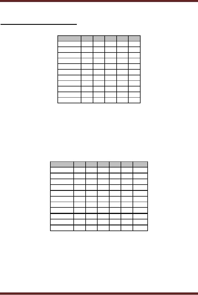
Table 13.1
Minterm
A
B
C
D
E
1
0
0
0
0
1
3
0
0
0
1
1
5
0
0
1
0
1
7
0
0
1
1
1
11
0
1
0
1
1
13
0
1
1
0
1
17
1
0
0
0
1
19
1
0
0
1
1
23
1
0
1
1
1
29
1
1
1
0
1
31
1
1
1
1
1
Table
13.1
Table of
Minterms representing Odd-Prime
Numbers
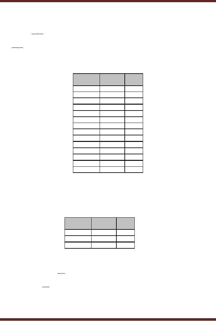
The
table of minterms is reorganized in
terms of groups of minterms
having 0, 1, 2, 3
and 4
1s. Table 13.2
· Minterms 1
has a single 1s
· Minterms
3, 5 and 17 have two 1s
each
· Minterms
7, 11, 13 and 19 have three
1s each
· Minterm 23
and 29 have 4 1s
· Minterm 31
has 5 1s
Minterm
A
B
C
D
E
used
1
0
0
0
0
1
3
0
0
0
1
1
5
0
0
1
0
1
17
1
0
0
0
1
7
0
0
1
1
1
11
0
1
0
1
1
13
0
1
1
0
1
19
1
0
0
1
1
23
1
0
1
1
1
29
1
1
1
0
1
31
1
1
1
1
1
Table
13.2
Reorganized
Minterms representing Odd-Prime
Numbers
In the
first step of Quine-McCluskey
method minterms are compared
to eliminate single
variables.
Minterm 1 is compared with
minterms 3, 5 and 17 in the
next group. Similarly,
each
of the 3
minterms 3, 5 and 17 are
compared with each of the
minterms in the next
group
having 3
1s, that is, minterms 7,
11, 13 and 19. Minterms 7,
11, 13 and 19 are compared
with
each of
the minterms in the next
group having 4 1s, that
is, minterms 23 and 29.
Finally, each
of the
two minterms 23 and 29 are
compared with the minterm 31
in the last group having
all
1s or 5
1s.
118
CS302 -
Digital Logic & Design
The
results of the comparisons
between minterms are
represented in a separate
table.
Table13.3.
The first column lists
the minterms that have
been compared together to
eliminate
common
variables. Terms 1 and 3
form a single term
eliminating variable D, forming
the
product
term ABCE
. The
comparison terms 1 and 3 are
marked as used in table
13.2.
Similarly,
terms 1 and 5 from a
single term eliminating
variable C, forming the
product
term
ABDE . Both these
terms are marked as used in
table 13.2. Similarly, terms
1, 17
eliminate
variable A, terms 3, 7 eliminate
variable C, terms 3, 11 eliminate
variable B and so
on.
Minterms
Variable
used
removed
1,3
2
1,5
4
1,17
16
3,7
4
3,11
8
3,19
16
5,7
2
5,13
8
17,19
2
7,23
16
13,29
16
19,
23
4
23,31
8
29,31
2
Table
13.3
Table of
minterms, Single variable
eliminated
As a result of
comparison a total of 14,
four variable product terms
are formed,
eliminating a
single variable from each
term. All the 14 terms
are represented in table
13.3.
The
exhaustive search for
finding Prime Implicants has
not completed. The results
of the
comparisons
between two terms in table
13.3 are represented in a
separate table. Table
13.4.
Minterms
Variable
used
removed
1,3,5,7
2,4
1,3,17,19
2,16
3,7,19,23
4,16
Table
13.4
Table of
minterms, Two variable
eliminated
The
first column lists the
terms that have been
compared together to
eliminate
common
variables. So terms, 1, 3, 5 and 7
form a single term
eliminating variables C and
D,
forming
the product term ABE . The comparison terms
1,3 and 5,7 are
marked as used in
table
13.3.
Similarly terms, 1, 3, 17 and 19
from a single term
eliminating variable A and D,
forming
the
product term BCE .
Both these terms are
marked as used in table
13.3. All the
product
terms in
table 13.3 are compared to
eliminate common variables. No
more comparisons of
terms
and elimination of variables
take place, thus the
Prime Implicants have been
found.
119
CS302 -
Digital Logic & Design
There
are 3 Prime Implicants in
table 13.4 and 5 Prime
Implicant in table 13.3.
The
eight
Prime Implicants are
represented by product terms ACDE , ACDE , BCDE , ACDE ,
ABCE
, ABE , BCE and BDE .
In the
second step of Quine-McCluskey
method the essential and
minimal Prime
Implicants
are found. The Prime
Implicants found in the
first step are listed in
left most column
of the
table. 13.5. All the
original minterms are listed
in the top row. In each
cell an x is marked
indicating
that the Prime Implicant
listed in the left column
covers the minterm mentioned
in
the
top row. Thus the
Prime Implicant ACDE covers the minterms 3
and 11. In other
words
minterms 3
and 11 all have the
product terms ACDE .
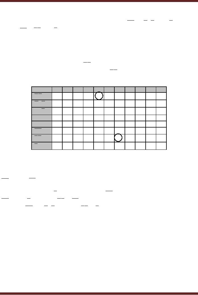
The table 13.5 can be
directly
implemented
from table 13.3 and
13.4.
1
3
5
7
11
13
17
19
23
29
31
x
x
ACDE
x
x
ACDE
x
x
BCDE
ACDE
x
x
ABCE
x
x
x
x
x
x
ABE
x
x
x
x
BCE
x
x
x
x
BDE
Table
13.5
Table of
Prime Implicants
Circles
are marked in cells having
x, which represent minterms
covered by only a
single
prime impicant. Thus the
minterms 11 and 17 are
covered by only the Prime
Implicants
ACDE and BCE respectively. These
implicants do not cover all
the minterms. The
other
essential
implicants that have minimum
number of variables and
which cover all the
remaining
BCDE , ACDE and ABE .
The simplified
expression is
minterms
are
ACDE + BCDE + ACDE
+
ABE + BCE . The function
can also be represented by
the
expression
ACDE + ACDE + ABCE
+
BCE + BDE . In both cases
the number of product
terms
is the
same with same number of
variables.
Combinational
Logic
Individual
gates AND, OR and NOT, NAND
and NOR Universal Gates
and XOR and
XNOR
gates perform unique
functions. These gates in
their individual capacity
can not
perform
any useful function. The
Logic Gates have to be
connected together in
different
combinations to
form Logic Circuits that
are able to perform some
useful operation like
addition ,
comparison etc. These
combinations of gates which
results in a circuit used
to
perform
some function are known as
Combinational Logic.
The
function of any Digital
Logic circuit is represented by
Boolean expressions. In
the
examples
discussed earlier, Boolean
expressions for various
functions have been
determined.
Two
forms of representing functions
through Boolean expressions
are the SOP and
POS
120
CS302 -
Digital Logic & Design
expressions.
These two types of Boolean
expressions are implemented
using a combination of
gates to
form Combinational Logic
Circuits.
Combinational
Circuit Implementation based on
SOP form
A standard
way to express a Boolean
expression is the SOP form.
The expression has
several
product terms which are
summed together through a
single OR gate. The
product
terms
can have variables and
their complemented form. A
SOP expression is implemented
by
using a
combinational circuit made up of
many AND gates and a single
OR gate (AND-OR
gate
combination). The inputs to
the AND gates can be in the
complemented form or the
un-
complemented
form, requiring the use of
NOT gates.
OR
Gate
level
AND
Gate
NOT
level
Gate
level
Figure
13.1
General,
Combination al Logic Circuit
based on SOP form
The
diagram shows the general
architecture of the SOP
Implementation. The
implementation
is based on three levels of
gates. SOP expression is
implemented by the
AND-OR
combination of gates. The AND
gates produce the product
terms. Outputs of all
the
AND gates
are connected to a single
multiple input OR gate for
sum of products. The
product
terms
comprise of literals in their
complemented form and
un-complemented form which
are
implemented by
NOT gates connected to the
inputs of the AND
gates.
Combinational
Circuit Implementation based on
POS form
A standard
way to express a Boolean
expression is the POS form.
The expression has
several
sum terms which are
multiplied together through a
single AND gate. The sum
terms
can
have variables and their
complemented form. A POS
expression is implemented by
using
a combinational
circuit made up of many OR
gates and a single AND gate
(OR-AND gate
combination).
The inputs to the OR gates
can be in the complemented
form or the un-
complemented
form, requiring the use of
NOT gates.
121
CS302 -
Digital Logic & Design
AND
Gate
level
OR
Gate
level
NOT
Gate
level
Figure
13.2
General,
Combination al Logic Circuit
based on POS form
The
diagram shows the general
architecture of the POS
Implementation. The
implementation
is based on three levels of
gates. POS expression is
implemented by the
OR-
AND combination
of gates. The OR gates
produce the sum terms.
Outputs of all the OR
gates
are
connected to a single multiple
input AND gate for product
of sum terms. The sum
terms
comprise of
literals in their complemented
form and un-complemented
form which are
implemented by
NOT gates connected to the
inputs of the OR
gates.
Design
and Implementation of Combinational
Circuits
The
design and implementation of a
combinational circuit starts by
defining the function
of the
Combinational circuit. The
function of a combinational circuit is
defined by a truth
table
or a function
table. Once the function
table is defined the
combinational circuit can be
directly
implemented
from the function
table.
Direct
implementation of a combinational circuit
from the function table
results in a
circuit
which uses maximum number of
gates organized at three
levels. This increases
the
cost,
the size of the circuit
and the power requirement of
the Combinational circuit.
The
propagation
delay of the circuit is of
the order of three gates.
Therefore, before
implementing
the
circuit the expression is
simplified using the manual
method by applying rules,
laws and
theorems of
Boolean Algebra or by the
Karnaugh map method or the
Quine-McCluskey
method if
the number of variables
exceeds 4.
Implementation of
an Adjacent 1s Detector
Circuit
A circuit
that checks an input number
and determines if it has two
adjacent 1s is
considered to
explain the entire process
of design and implementation of a
typical
Combinational
Logic Circuit. The Adjacent
1s detector circuit is implemented
using the
standard
SOP and POS forms of
Boolean expressions. The
circuit is also implemented
using
the
simplified Boolean expressions.
The alternate form of
implementing the circuit
using only
NAND or NOR
gates is also
discussed.
122
CS302 -
Digital Logic & Design
1. SOP
based Implementation of the
Adjacent 1s Detector
Circuit
The
Adjacent 1s Detector accepts
4-bit inputs. If two
adjacent 1s are detected in
the
input,
the output is set to high.
The operation of the
Adjacent 1s Detector is represented by
the
function
table. Table 13.6. In the
function table, for the
input combinations 0011,
0110, 0111,
1011,
1100, 1101, 1110 and
1111 the output function is
a 1.
Input
Output
Input
Output
A
B
C
D
F
A
B
C
D
F
0
0
0
0
0
1
0
0
0
0
0
0
0
1
0
1
0
0
1
0
0
0
1
0
0
1
0
1
0
0
0
0
1
1
1
1
0
1
1
1
0
1
0
0
0
1
1
0
0
1
0
1
0
1
0
1
1
0
1
1
0
1
1
0
1
1
1
1
0
1
0
1
1
1
1
1
1
1
1
1
Table
13.6
Function
Table of Adjacent 1s
Detector
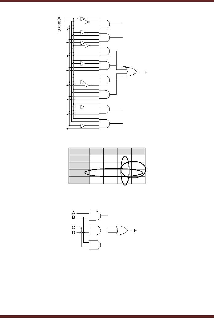
Implementing
the circuit directly from
the function table based on
the SOP form
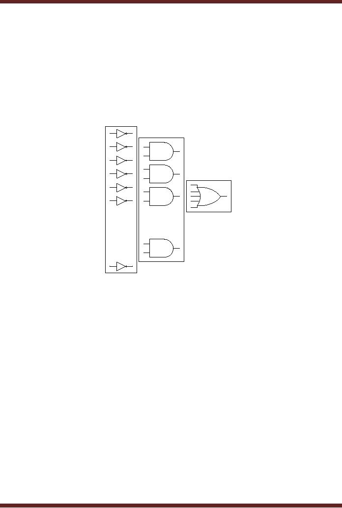
requires 8 AND
gates for the 8 product
terms (minterms) with an
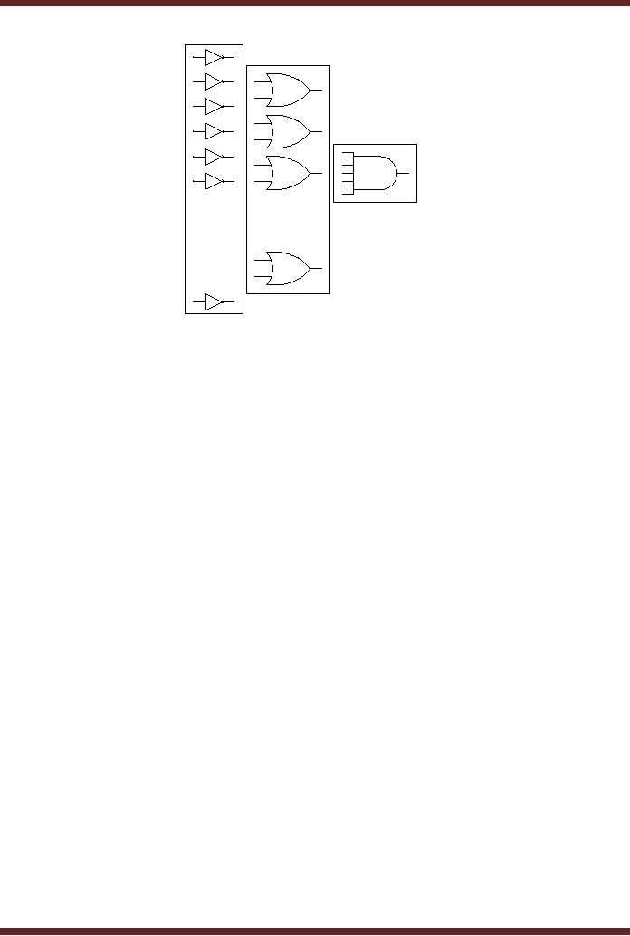
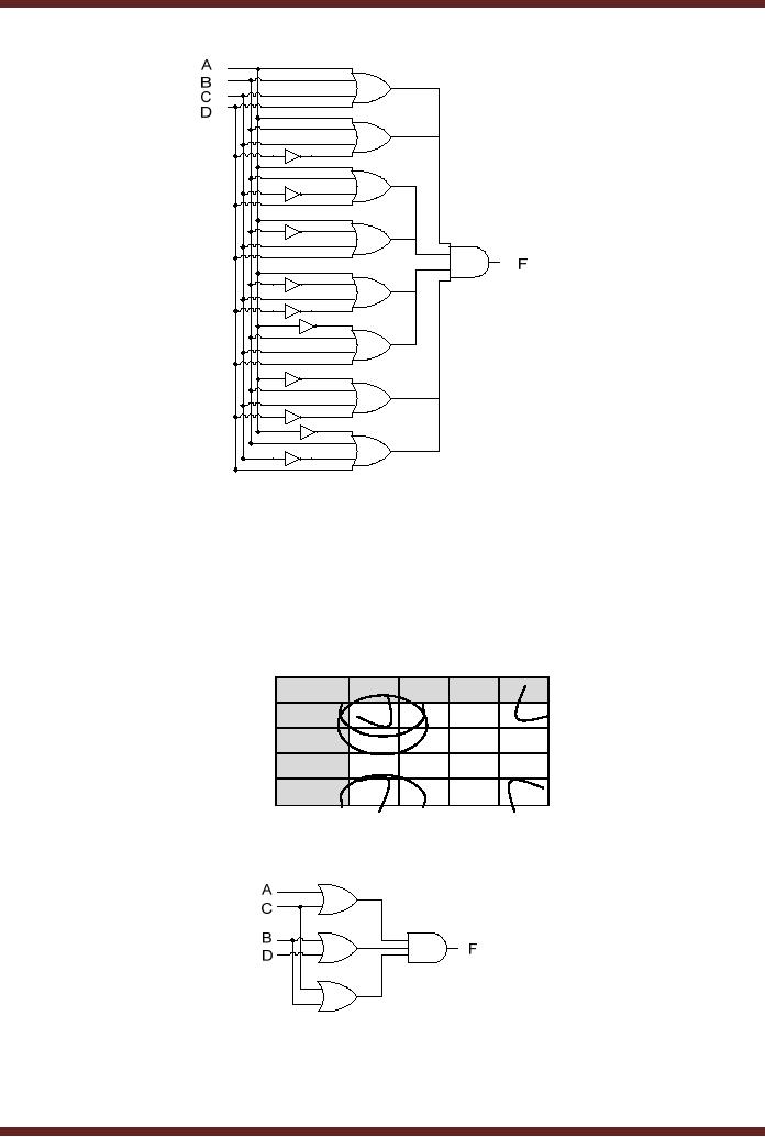
8-input OR gate. Figure
13.3.
The
total gate count is
· One 8
input OR gate
· Eight 4
input AND gates
· Ten
NOT gates
The
expression can be simplified
using a Karnaugh map, figure
13.4, and then
the
simplified
expression can be implemented to
reduce the gate count.
The simplified
expression
is AB + CD + BC . The circuit
implemented using the
expression AB
+
CD + BC has
reduced
to 3 input OR
gate and 2 input AND gates.
Figure 13.5
123
CS302 -
Digital Logic & Design
Figure
13.3
SOP
Implementation of Adjacent 1s
Detector
AB\CD
00
01
11
10
1
00
0
0
0
01
0
0
1
1
11
1
1
1
1
10
0
0
1
0
Figure
13.4
Simplification
of Adjacent 1s Detector SOP
Boolean Expression
Figure
13.5
Simplified
SOP based Adjacent 1s
Detector
The
simplified Adjacent 1s Detector
circuit uses only four
gates reducing the cost,
the
size of
the circuit and the
power requirement. The
propagation delay of the
circuit is of the
order of
two gates.
The
simplified Adjacent 1s Detector
circuit can be implemented
using only NAND
Gates.
The AND-OR combinational
circuit can be easily
replaced by a NAND based
implementation
without changing the number
of gates. Figure
13.6.
124
CS302 -
Digital Logic & Design
Figure
13.6
NAND based
Adjacent 1s Detector
Bubbles
representing NOT gates are
placed at the output of the
three AND gates.
Converting
the three AND gates to NAND
gates. To balance out the
three NOT gates added
at
the
outputs of the three AND
gates, three bubbles
representing three NOT gates
are also
placed at
the three inputs of the OR
gate. The Resulting OR gate
symbol with three bubbles
at
the
three inputs is an alternate
symbol for a three input
NAND gate.
Implementing
Combinational Logic Circuits
using only NAND gates helps
in reducing
the
circuit size and cost as
the Integrated Circuit
packages multiple gates in a
single package.
If,
for example, the 3-input
NAND gate in the circuit had
been a 2-input NAND gate,
only a
single IC
package (74LS00) would have
been required. For the
circuit shown in figure 13.5
two
separate IC
packages (74LS08 and 74LS32)
are required.
2. POS
based Implementation of the
Adjacent 1s Detector
Circuit
A combinational
Adjacent 1s Detector circuit
can be implemented, based on
the POS
form. It
was discussed earlier that
it is very easy to switch
between SOP and the
POS
representations
using the information in a
function table or the
information mapped to a
Karnaugh
Map. Referring to the
Function Table for the
Adjacent 1s Detector. Table
13.6 a
POS
based Adjacent 1s Detector
circuit can be easily
implemented by using the Sum
terms
(Maxterms).
The POS based circuit
for this particular case
has 8 sum terms which
require 8
OR gates
and a single 8-input AND
gate. Figure 13.7. The
total gate count is
· One 8
input AND gate
· Eight 4
input OR gates
· Ten
NOT gates
Both,
the SOP based circuit
discussed earlier and the
POS based circuit give
identical
outputs
for identical set of input
combinations. One practical
purpose of using either the
SOP
or the
POS based implementation is to
reduce the size of the
circuit and have a simpler
circuit.
In the
example of Adjacent 1s Detector
circuit both the SOP
and POS based
implementations
have
equal number of minterms (8)
and maxterms (8) thus
both implementation use
exactly
the
same number of gates (19).
In many cases, the function
describing the operation of
a
combinational
circuit has minterms which
are either less than or
more than the number
of
maxterms.
Thus it is wiser to choose
the implementation form that
uses the least number
of
minterms or
maxterms to achieve a combinational
circuit that uses the
least number of
gates.
125
CS302 -
Digital Logic & Design
Figure
13.7
POS
Implementation of Adjacent 1s
Detector
The
POS expression can be
simplified using a Karnaugh
map. Figure 13.8, the
simplified
expression
can be implemented to reduce
the gate count. The
simplified expression is
(A + C)(B + C)(B + D)
AB\CD
10
00
01
11
00
0
0
1
0
01
0
0
1
1
11
1
1
1
1
10
0
0
1
0
Figure
13.8
Simplification
of Adjacent 1s Detector POS
Boolean Expression
Figure
13.9
Simplified
POS based Adjacent 1s
Detector
126
CS302 -
Digital Logic & Design
The
simplified Adjacent 1s Detector
circuit uses only four
gates reducing the cost,
the
size of
the circuit and the
power requirement. The
propagation delay of the
circuit is of the
order of
two gates.
The
simplified Adjacent 1s Detector
circuit can be implemented
using only NOR
Gates.
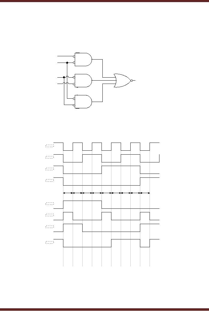
The
OR-AND combinational circuit
can be easily replaced by a
NOR based
implementation
without
changing the number of
gates. Figure 13.10.
Figure
13.10
NOR
based Adjacent 1s
Detector
Bubbles
representing NOT gates are
placed at the output of the
three OR gates,
converting
the three OR gates to NOR
gates. To balance out the
three NOT gates added
at
the
outputs of the three OR
gates, three bubbles
representing three NOT gates
are also
placed at
the three inputs of the AND
gate. The Resulting AND gate
symbol with three
bubbles
at the
three inputs is an alternate
symbol for a three input
NOR gate.
Operation of
Adjacent 1s detector
Circuit
The
operation of a Combinational Logic
Circuit can be verified by
applying varying set
of signals at
the input of the circuit
and comparing the output of
the combinational circuit
with
the
corresponding outputs in the
Function Table. If the
varying set of inputs and
the
corresponding
outputs are plotted over a
period of time, the timing
diagram thus
obtained,
describes
the operation of the
circuit. Figure 13.11
Figure
13.11 Timing Diagram of the
Adjacent 1s Detector
127

CS302 -
Digital Logic & Design
To prove
that the SOP and
POS based Adjacent 1s
Detector combinational
circuits
synthesized
from the Function table.
Table 13.6 are identical,
the timing diagram, figure
13.11
is based on
the operation of the POS
based simplified circuit.
Figure 13.9
The
timing diagram is for time
intervals t0 to t8. A, B, C and D
are the inputs to
the
circuit
which are shown changing
with time. The timing
signals 1, 2 and 3 represent
the
outputs of
the OR gates 1, 2 and 3. The
timing signal F represents
the output of the
circuit.
At interval t0
the input ABCD to the
circuit is 0000, the outputs
of the three OR gates
is
0, 0 and 0
and the circuit output is
also 0. At the interval t3
the input ABCD to the
circuit is
0011,
the outputs of OR gates 1, 2
and 3 are 111. The
output F is also a 1, which
indicates
adjacent
1s. At interval t6 the input
ABCD to the circuit is 0110,
the outputs of OR gates 1,
2
and 3
are 111. The output F is
again 1 indicating adjacent
1s.
The
operation of the circuit
which is based on the POS
simplified expression
also
proves
that a POS based expression
determined from the truth
table and K-map results in
a
circuit
which operates in an identical
manner to that of a SOP
based circuit.
Active
low/high Inputs and
Outputs
The
circuits discussed so far
have their output set to
when to indicate an active
state.
For
example, the output of the
BCD to 7-Segment Decoder
circuit has its seven
segment
outputs
set to 1 to indicate a segment
that has been selected.
Similarly, the
Comparator
circuit's
three outputs are normally
at binary 0. The appropriate
output is set to 1 to
indicate
the
relationship between the two
numbers. The Odd-Prime
Number detector circuit
output
normally is
set at 0. It is activated to 1 to
indicate an Odd-Prime number.
The Adjacent 1s
Detector
circuit also sets its
output to active 1 to indicate
detection of Adjacent 1s.
All the four
circuits
have an active-high output.
That is, normally the
output is at logic 0. The
output is set
to 1 to indicate
an active state.
Combinational
circuits can have an
active-high output or an active-low
output. An
active-high or
active-low output doesn't
effect the operation of the
combinational circuit in
any
manner. To
convert a circuit having an
active-high output to active
low-output requires
the
inversion of
the circuit output by
connecting a NOT gate.
Symbolically, a bubble is added
to
the
circuit output. Thus,
circuits having a bubble at
their outputs are considered
to have an
active-low
output.
Circuits
can also have active-high or
active-low inputs. The
operation of the
circuits
having an
active-high input is not any
different from that of an
active-low input circuit.
Active-
low
input circuits are activated
on a logic 0 input. Circuits
having an active-low input
have
bubbles
connected to circuits inputs.
The four circuits discussed
so far have active-high
inputs.
The
four logic gates AND,
OR, NAND and NOR can be
described in terms of their
input
and
output logic levels. The AND
gate doesn't have any
bubbles at its inputs or
output. The
AND gate
performs AND operation on two
active high inputs to result
in an active high
output.
The OR
gate also doesn't have
any bubbles at its inputs
and output. OR gate performs
OR
operation on
two active high inputs to
result in an active high
output. The NAND and
NOR
gates
have a bubble at their
outputs. Their operation can
be described in terms of AND
and
OR gates. NAND
gate performs AND operation on
two active high inputs
resulting in an active
low
output. The NOR gate
performs OR operation on two
active high inputs to result
in an
active
low output
128
CS302 -
Digital Logic & Design
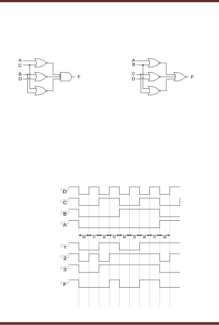
To help
understand active-low input,
consider the active-high
input and active-high
output
SOP circuit. Fig. 13.5
which is converted into an
active-low input and output
circuit by
connecting
NOT gates at the circuit
inputs and outputs. Figure
13.12. The circuit operation
is
verified
with the help of a timing
diagram. Figure
13.13.
A
1
B
C
2
F
D
3
Figure
13.12
SOP
based active-low input and
output Adjacent 1s
Detector
D
C
B
A
t0
t1
t2
t3
t4
t5
t6
t7
t8
1
2
3
F
Figure
13.13 Timing Diagram of the
active-low input/output Adjacent 1s
Detector
The
timing diagram describes the
operation of the circuit for
the intervals t0 to t8.
The
timing
signals A, B, C and D represent
the active-low inputs
applied at the inputs. The
timing
signals 1, 2
and 3 represent the outputs
of the NOR gates 1, 2 and 3
respectively, shown in
their
alternate symbolic form. The
timing signal F represents
the active-low
output.
129

CS302 -
Digital Logic & Design
At interval t0
the active-low input at
inputs ABCD is 0000 which
actually represents
1111.
The active-low output F is 0
which indicates that
adjacent 1s have been
detected.
Similarly at
intervals t1 to t4, the
active-low inputs ABCD 0001,
0010, 0011 and 0100
actually
represent
the numbers 1110, 1101,
1100 and 1011, the
output is 0 indicating that
adjacent 1s
have
been detected.
Implementation of
an Odd-Parity Generator
Circuit
Consider
the second example of a
circuit to generate odd
parity. The circuit checks
an
8-bit
number and generates a
parity bit to fulfil the
Odd-Parity condition. The
8-bit data and
the
parity
bit are communicated to the
receiver circuit. The
receiver circuit checks the
8-bit data
and
the parity bit to determine
if an error has
occurred.
The
first step in implementing
any circuit is to represent
its operation in terms of a
Truth
or Function
table. The function table
for an 8-bit data as input
has 28 has 256
input
combinations,
which becomes unmanageable.
Therefore, for the sake of
simplicity a 4-bit
data
with
odd parity is assumed. The
receiver circuit is also
based on the 4-bit
data.
130
Table of Contents:
- AN OVERVIEW & NUMBER SYSTEMS
- Binary to Decimal to Binary conversion, Binary Arithmetic, 1s & 2s complement
- Range of Numbers and Overflow, Floating-Point, Hexadecimal Numbers
- Octal Numbers, Octal to Binary Decimal to Octal Conversion
- LOGIC GATES: AND Gate, OR Gate, NOT Gate, NAND Gate
- AND OR NAND XOR XNOR Gate Implementation and Applications
- DC Supply Voltage, TTL Logic Levels, Noise Margin, Power Dissipation
- Boolean Addition, Multiplication, Commutative Law, Associative Law, Distributive Law, Demorgans Theorems
- Simplification of Boolean Expression, Standard POS form, Minterms and Maxterms
- KARNAUGH MAP, Mapping a non-standard SOP Expression
- Converting between POS and SOP using the K-map
- COMPARATOR: Quine-McCluskey Simplification Method
- ODD-PRIME NUMBER DETECTOR, Combinational Circuit Implementation
- IMPLEMENTATION OF AN ODD-PARITY GENERATOR CIRCUIT
- BCD ADDER: 2-digit BCD Adder, A 4-bit Adder Subtracter Unit
- 16-BIT ALU, MSI 4-bit Comparator, Decoders
- BCD to 7-Segment Decoder, Decimal-to-BCD Encoder
- 2-INPUT 4-BIT MULTIPLEXER, 8, 16-Input Multiplexer, Logic Function Generator
- Applications of Demultiplexer, PROM, PLA, PAL, GAL
- OLMC Combinational Mode, Tri-State Buffers, The GAL16V8, Introduction to ABEL
- OLMC for GAL16V8, Tri-state Buffer and OLMC output pin
- Implementation of Quad MUX, Latches and Flip-Flops
- APPLICATION OF S-R LATCH, Edge-Triggered D Flip-Flop, J-K Flip-flop
- Data Storage using D-flip-flop, Synchronizing Asynchronous inputs using D flip-flop
- Dual Positive-Edge triggered D flip-flop, J-K flip-flop, Master-Slave Flip-Flops
- THE 555 TIMER: Race Conditions, Asynchronous, Ripple Counters
- Down Counter with truncated sequence, 4-bit Synchronous Decade Counter
- Mod-n Synchronous Counter, Cascading Counters, Up-Down Counter
- Integrated Circuit Up Down Decade Counter Design and Applications
- DIGITAL CLOCK: Clocked Synchronous State Machines
- NEXT-STATE TABLE: Flip-flop Transition Table, Karnaugh Maps
- D FLIP-FLOP BASED IMPLEMENTATION
- Moore Machine State Diagram, Mealy Machine State Diagram, Karnaugh Maps
- SHIFT REGISTERS: Serial In/Shift Left,Right/Serial Out Operation
- APPLICATIONS OF SHIFT REGISTERS: Serial-to-Parallel Converter
- Elevator Control System: Elevator State Diagram, State Table, Input and Output Signals, Input Latches
- Traffic Signal Control System: Switching of Traffic Lights, Inputs and Outputs, State Machine
- Traffic Signal Control System: EQUATION DEFINITION
- Memory Organization, Capacity, Density, Signals and Basic Operations, Read, Write, Address, data Signals
- Memory Read, Write Cycle, Synchronous Burst SRAM, Dynamic RAM
- Burst, Distributed Refresh, Types of DRAMs, ROM Read-Only Memory, Mask ROM
- First In-First Out (FIFO) Memory
- LAST IN-FIRST OUT (LIFO) MEMORY
- THE LOGIC BLOCK: Analogue to Digital Conversion, Logic Element, Look-Up Table
- SUCCESSIVE APPROXIMATION ANALOGUE TO DIGITAL CONVERTER