 |

CS302 -
Digital Logic & Design
Lesson
No. 28
TIMING
DIAGRAM OF A SYNCHRONOUS DECADE
COUNTER
CLOCK
Input
F0
Output
F1
Output
F2
Output
F3
Output
t2
t3
t4
t5
t6
t7
t8
t10
t9
t1
Figure
28.1
Timing
diagram of a Synchronous Decade
Counter
Mod-n
Synchronous Counter
A Mod-n
Synchronous can be implemented
using appropriate number of
J-K flip-flops
connected
together with their clocks
triggered simultaneously. A synchronous
counter which
counts a
truncated sequence of n unique
states can be similarly
implemented. The
Modulus
number
represents the unique number
of states which the counter
counts in a sequence.
The
Modulus
number determines the number
of flip-flops required based on
the relation n = 2m
where m is
the number of
flip-flops.
284
CS302 -
Digital Logic & Design
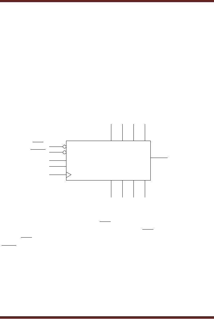
Integrated
Circuit Synchronous
Counters
Instead of
connecting a large number of
flip-flops together to form
large Synchronous
counters,
counter circuits available in
Integrated Circuit form can
be quickly connected to
form
large
counters. The 74HC163 is a
4-bit Synchronous Counter.
Figure 28.2. The counter
has
the
following pins.
1.
Parallel
data inputs D0, D1, D2 and D3
2.
Data
outputs Q0, Q1, Q2 and Q3
3.
Positive
edge-triggered CLOCK
signal
4.
Active-low
CLR input which resets
the Counter output to
0000
5.
Active-low
LOAD input which loads
the 4-bit data applied at
the counter inputs
6.
Active-high
ENT and ENP enable
inputs. For the counter to
operate both the enable
inputs
have to be
high
7. The
Ripple Clock Output RCO
goes high when the
Counter reaches the terminal
count
1111.
The RCO output along
with ENT and ENP
enable input pins are
used to cascade
multiple
counter ICs for implementing
larger counters
D0 D1 D2 D3
CLR
LOAD
RCO
74HC163
ENT
ENP
CLK
Q0 Q1 Q2 Q3
Figure
28.2a 74HC163 4-bit
Synchronous Counter
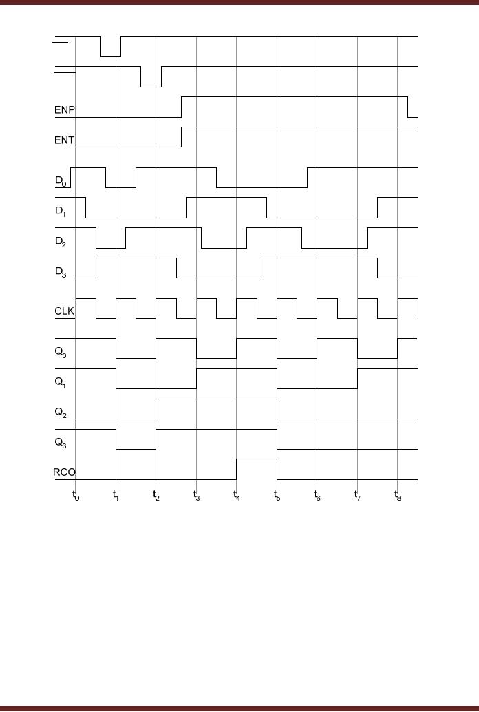
Referring to
the timing diagram, the
CLR signal is
activated between interval t0 and t1.
The
counter output is reset
synchronously at interval t1 as the CLR signal is active at
interval
t1. If the CLR signal is deactivated before
interval t1
then
the counter output is not
reset. The
LOAD
signal is
activated between interval t1 and t2. At
the clock transition at t2, the counter is
loaded
with the 4-bit data
applied at the inputs D0, D1, D2 and
D3. The ENP
and ENT enable
signals
are activated before
interval t3
and
the counter increments to
the higher count at
clock
transition at
intervals t3
and t4. When the counter
reaches the count 15 at
interval t4,
the RCO
(Ripple
Clock Output) is set to high
indicating that terminal
count has been reached.
At
intervals
t5, t6, t7 and t8
the
counter successively counts to 0, 1, 2
and 3. The counter
enable
signal
ENP is deactivated after
interval t8,
which inhibits the counter
from counting any
further.
285
CS302 -
Digital Logic & Design
CLR
LOAD
Figure
28.2b Timing diagram of the
74HC163 Synchronous
counter
The
74HC160 is a 4-bit Synchronous
Decade counter with the
same input and
output
pins as
the 74HC163. The RCO
output of the decade counter
is activated when the
counter
reaches
its terminal count
1001.
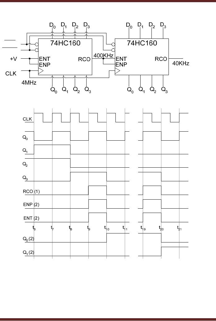
Cascading
Counters
It is very
convenient to cascade Integrated
Circuit counters together to
form larger
counters
instead of connecting together
flip-flops to implement a large
counter. The enable
inputs
and Ripple Clock Outputs of
the Integrated Circuit
counters allow cascading of
multiple
counters
together. Two, 74HC160
decade counters are shown
connected together to
divide
the
input frequency by 10 and
100. Figure 28.3. The
74HC163 can also be
similarly cascaded
together.
286
CS302 -
Digital Logic & Design
CLR
LOAD
Figure
28.3a Cascaded Decade
Counters
Figure
28.3b Timing diagram of a
Cascaded Decade
Counter
In the
timing diagram, at interval t9 the first decade
counter reaches the terminal
count 1001.
The
RCO output of the counter is
set to logic 1. The RCO of
the first counter is
connected to
the
ENP and ENT enable
pins of the second counter,
therefore the counter is
enabled. At
interval
t10 on a positive
clock transition the first
counter increments to count
0000. Since the
second
counter is also enabled, it is
incremented to 0001. As soon as
the first counter is
incremented to
0000, the ECO signal is
deactivated which in-turn
also inhibits the
second
counter.
The first counter counts
from 0001 to 1000 in the
intervals t11
to t19. At interval t19 the
287
CS302 -
Digital Logic & Design
first
counter again reaches its
terminal count 1001, the
RCO output of counter once
again
becomes
active thereby activating
the second counter. At
interval t20
on a positive
clock
transition
the first and second
counters increment to count
0000 and 0010 respectively.
The
RCO
signal is again deactivated
inhibiting the second
counter from counting. This
sequence
continues
after the first counter
reaches its terminal
count.
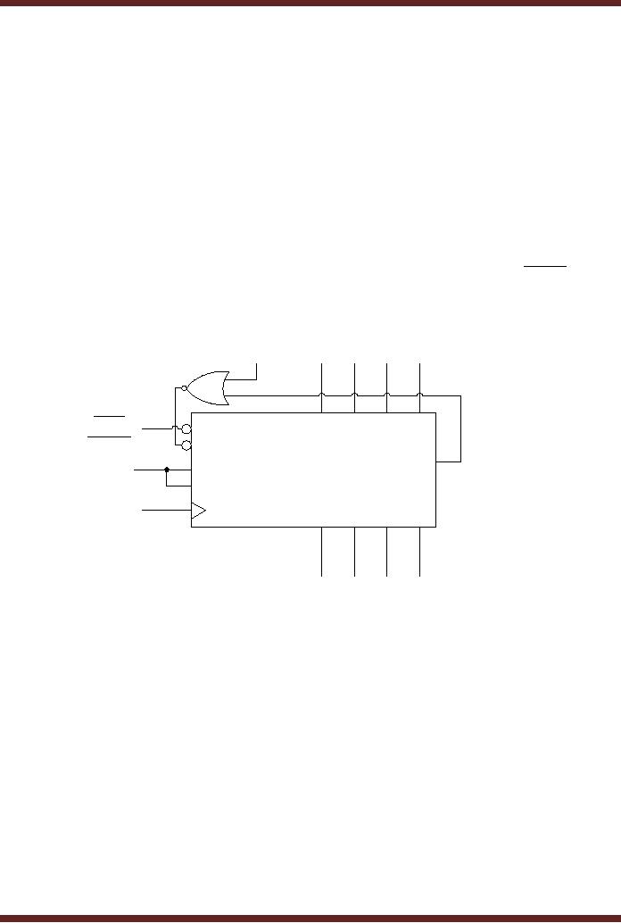
Integrated
Circuit Counters with
Truncated Sequences
Earlier, a
decade counter was
implemented by truncating the
counting sequence of a
MOD-16
counter. The Integrated
Circuit Counters can also be
configured as MOD-n
counters
where n
represents the truncated
sequence and is less than
16. Figure 28.4 shows
the circuit
diagram of
the 74HC163 counter
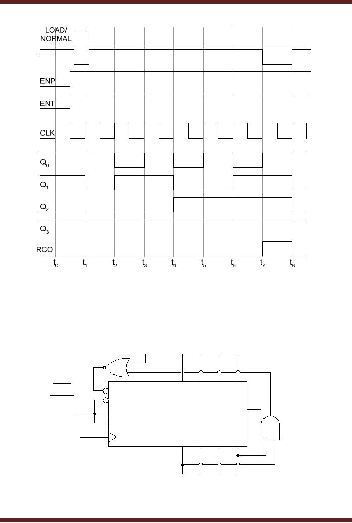
configured as Mod-7 counter.
The counter is preset with
the
count
value 1001 by setting the
LOAD/NORMAL input to logic 1 at
the NOR gate input. At
the
positive
clock transition t1, the
count value is loaded. The
counter increments and at
interval t7
it reaches
the terminal count. The
RCO output is set to logic 1
which sets the LOAD input to
logic 0. At
the positive clock
transition at interval t8 the preset value
1001 is reloaded and
the
counter
continues its counting
sequence.
D0 D1 D2 D3
LOAD/NORMAL
1/0
1001
CLR
LOAD
RCO
74HC163
ENT
+V
ENP
CLK
Q0 Q1 Q2 Q3
Figure
28.4a 74HC163 configured as
Mod-7 counter
288
CS302 -
Digital Logic & Design
LOAD
Figure
28.4b The timing diagram of
a truncated Mod-7
Counter
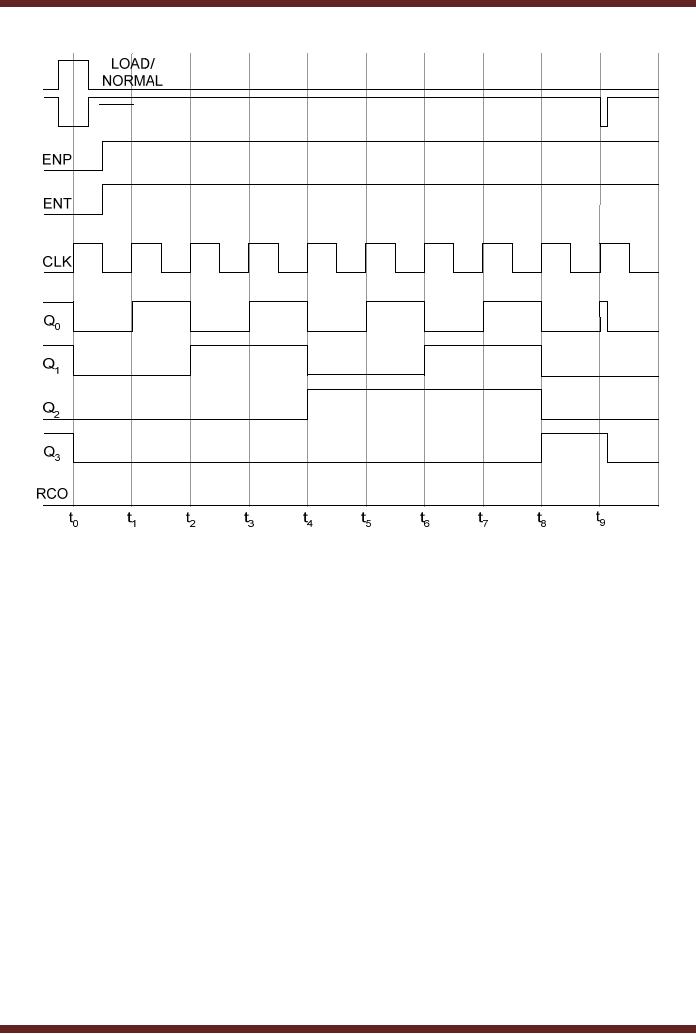
Another
method to configure an Integrated
Circuit counter is to reset
the counter when
it reaches
the maximum count value of
its truncated sequence. This
requires extra logic in
the
form of
logic gates that determine
the terminating state and
reset the counter. The
circuit
diagram of
the counter is shown. Figure
28.5
D0 D1 D2 D3
LOAD/NORMAL
1/0
CLR
LOAD
RCO
74HC161
ENT
+V
ENP
CLK
Q0 Q1 Q2 Q3
Figure
28.5a 74HC161 configured as
Mod-9 counter
289
CS302 -
Digital Logic & Design
CLR
Figure
28.5b Timing diagram of a
74HC161 configured as Mod-9
counter
The
counter used is 74HC161
instead of 74HC163. The
74HC161 has an
Asynchronous
Clear input, where as the
74HC163 counter has a
synchronous Clear input.
At
time
interval t9
the
counter increments to 1001
which sets the output of
the AND gate to logic
1. The
NOR gate output is set to
logic low which activates
the clear input and
resets the
counter to
0000. The 74HC163 counter
which has a synchronous
clear input, will reset
counter
resets at
interval t10
when
there is a transition at the
clock input. It is clear
from the timing
diagram
that to implement a Mod-9
counter the 74HC161 instead
of 74HC163 counter has
to
be
used.
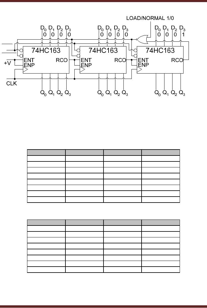
Cascaded
Counters with Truncated
Sequences
Cascaded
counters can also be
configured to count in a truncated
sequence. The
circuit
diagram of three cascaded
74HC163 is shown. Figure
28.6. The 12-bit
cascaded
counter is
loaded with initial count
value 1000 0000 0000.
When the counter counts to
1111
1111
1111, the RCO output
set to logic 1 by the third
counter reloads the initial
count values
0000,
0000 and 1000 in all
the three counters
respectively. The 12-bit
counter can be
configured
for maximum count sequence
as Modulus 4096 counter. The
counter has been
configured to
count from 1000 0000
0000 to 1111 1111 1111
that is 2048 states or
Modulus
2048
counter.
290
CS302 -
Digital Logic & Design
CLR
LOAD
Figure
28.6
74HC163
counters connected for
cascaded truncated count
sequence
Up-Down
Counter
An up-down
counter can increment its
output count value at each
clock transition or
decrement
its count value at each
clock transition, depending
upon the count mode it
is
configured
in. The counter can be
reconfigured to count in the
opposite direction during
its
count
sequence. The circuit of an
up-down 3-bit counter can be
developed by studying the
up-
down
count sequence of the
counter. Table 28.1.
Clock
Pulse
Q2
Q1
Q0
0
0
0
0
1
0
0
1
2
0
1
0
3
0
1
1
4
1
0
0
5
1
0
1
6
1
1
0
7
1
1
1
Table
28.1a
Up-counting
sequence of a 3-bit Synchronous
Counter
Clock
Pulse
Q2
Q1
Q0
0
1
1
1
1
1
1
0
2
1
0
1
3
1
0
0
4
0
1
1
5
0
1
0
6
0
0
1
7
0
0
0
Table
28.1b Down-counting sequence of a
3-bit Synchronous
Counter
A 3-bit
Synchronous up-counter has
been discussed earlier.
Consider the implementation
of
down-counter,
the up and down counter
can be combined to form a
single configurable
up-
down
counter. For the
down-counting sequence the
output Q0
of the
first flip-flop
toggles
291

CS302 -
Digital Logic & Design
between 0
and 1, therefore the J-K
inputs are connected to
logic 1. The output Q1 of the
second
flip-flop toggles between
logic 0 and 1 when the
Q0 output is logic 0
or Q 0 is logic
1.
The
output Q2
of the
third flip-flop toggles when
Q0 and Q1 outputs are both
logic 0 or Q
0 and
Q1 are
both logic 1.
292
Table of Contents:
- AN OVERVIEW & NUMBER SYSTEMS
- Binary to Decimal to Binary conversion, Binary Arithmetic, 1s & 2s complement
- Range of Numbers and Overflow, Floating-Point, Hexadecimal Numbers
- Octal Numbers, Octal to Binary Decimal to Octal Conversion
- LOGIC GATES: AND Gate, OR Gate, NOT Gate, NAND Gate
- AND OR NAND XOR XNOR Gate Implementation and Applications
- DC Supply Voltage, TTL Logic Levels, Noise Margin, Power Dissipation
- Boolean Addition, Multiplication, Commutative Law, Associative Law, Distributive Law, Demorgans Theorems
- Simplification of Boolean Expression, Standard POS form, Minterms and Maxterms
- KARNAUGH MAP, Mapping a non-standard SOP Expression
- Converting between POS and SOP using the K-map
- COMPARATOR: Quine-McCluskey Simplification Method
- ODD-PRIME NUMBER DETECTOR, Combinational Circuit Implementation
- IMPLEMENTATION OF AN ODD-PARITY GENERATOR CIRCUIT
- BCD ADDER: 2-digit BCD Adder, A 4-bit Adder Subtracter Unit
- 16-BIT ALU, MSI 4-bit Comparator, Decoders
- BCD to 7-Segment Decoder, Decimal-to-BCD Encoder
- 2-INPUT 4-BIT MULTIPLEXER, 8, 16-Input Multiplexer, Logic Function Generator
- Applications of Demultiplexer, PROM, PLA, PAL, GAL
- OLMC Combinational Mode, Tri-State Buffers, The GAL16V8, Introduction to ABEL
- OLMC for GAL16V8, Tri-state Buffer and OLMC output pin
- Implementation of Quad MUX, Latches and Flip-Flops
- APPLICATION OF S-R LATCH, Edge-Triggered D Flip-Flop, J-K Flip-flop
- Data Storage using D-flip-flop, Synchronizing Asynchronous inputs using D flip-flop
- Dual Positive-Edge triggered D flip-flop, J-K flip-flop, Master-Slave Flip-Flops
- THE 555 TIMER: Race Conditions, Asynchronous, Ripple Counters
- Down Counter with truncated sequence, 4-bit Synchronous Decade Counter
- Mod-n Synchronous Counter, Cascading Counters, Up-Down Counter
- Integrated Circuit Up Down Decade Counter Design and Applications
- DIGITAL CLOCK: Clocked Synchronous State Machines
- NEXT-STATE TABLE: Flip-flop Transition Table, Karnaugh Maps
- D FLIP-FLOP BASED IMPLEMENTATION
- Moore Machine State Diagram, Mealy Machine State Diagram, Karnaugh Maps
- SHIFT REGISTERS: Serial In/Shift Left,Right/Serial Out Operation
- APPLICATIONS OF SHIFT REGISTERS: Serial-to-Parallel Converter
- Elevator Control System: Elevator State Diagram, State Table, Input and Output Signals, Input Latches
- Traffic Signal Control System: Switching of Traffic Lights, Inputs and Outputs, State Machine
- Traffic Signal Control System: EQUATION DEFINITION
- Memory Organization, Capacity, Density, Signals and Basic Operations, Read, Write, Address, data Signals
- Memory Read, Write Cycle, Synchronous Burst SRAM, Dynamic RAM
- Burst, Distributed Refresh, Types of DRAMs, ROM Read-Only Memory, Mask ROM
- First In-First Out (FIFO) Memory
- LAST IN-FIRST OUT (LIFO) MEMORY
- THE LOGIC BLOCK: Analogue to Digital Conversion, Logic Element, Look-Up Table
- SUCCESSIVE APPROXIMATION ANALOGUE TO DIGITAL CONVERTER