 |
CS302 -
Digital Logic & Design
Lesson
No. 40
DECODING
LARGE MEMORIES
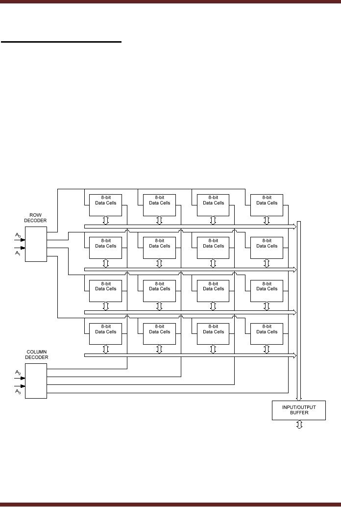
Large
memories such as the 16 KB
memory have row and
column decoders that
split
the
input address into a row
address and a column address
and activate a row and
column
select
lines respectively. The row
and column select lines
select a location in the
memory
array.
The memory is arranged in a
two-dimensional manner instead of
the linear address
method
discussed earlier. The
reason for adopting a row
and column decoder to
independently
but simultaneously select a
location by its unique row
and column number is
to
speed up
the decoding process. As the
memories get larger the
decoders that decode
and
select a
unique memory location also
become very large with
large number of gates. Due
to
the
increased level of gates of
the decoding circuitry the
delay in decoding the input
address
increases,
thereby slowing the memory
access. A large address
split into row and
column
addresses
and separately decoded by
row and column decoders
requires comparatively
smaller
decoders with fewer number
of gates resulting in fast
decoding times and
thereby
faster
memory access. The block
diagram of a memory using
row and column decoders
is
shown.
Figure 40.1.
Figure
40.1
Memory
array decoded by Row and
Columns Decoders
Detail
circuitry of the Input/Output
Buffer is shown which
manages the control of
the
Data In
and Data Out lines.
Figure 40.2. When the W,
write signal is active and
the memory
chip is
selected CS, the top AND
gate is selected and the
bottom AND gate is disabled.
The
data
applied at the Data In/Out
bi-directional lines is stored in
the selected latches. When
the
W signal is
inactive and the CS and OE
signals are active the
bottom AND gate is
selected
403

CS302 -
Digital Logic & Design
which
enables the tri-state
buffers connected at the end
of the data out lines
leading from the
latch
outputs. This allows data
from the selected latches to
be available on the Data
In/Out
lines.
Figure
40.2
Input/Output
Data Circuit
The
Reading and Writing of data
is done by activating the
various memory signals in
a
proper
sequence. The Memory Read
Cycle controls the memory
for reading of data and
a
Memory
Write Cycle controls the
memory for writing of
data.
Memory
Read Cycle
The
timing diagram of the read
cycle is shown. Figure 40.3.
To read data from
the
memory,
the Read Cycle is initiated
by applying the address
signals. The valid address
needs
to be maintained
stable for a specified
duration tRC
the
read cycle time. Next,
the CS
and
the OE signals are activated,
after a delay of tGQ, the
output enable access time
measured with
respect to
the high-to-low transition of
the OE
signal,
valid data appears on the
data lines.
The
tAQ, address access
time is measured from the
beginning of the valid
address that
appears on
the address lines to the
appearance of valid data on
the data lines. The
time tEQ
measures
the chip enable access
time which is the time
for the valid data to
appear after the
high-to-low
transition of the chip
select signal CS .
Memory
Write Cycle
The
timing diagram of the write
cycle is shown. Figure 40.4.
To write data to the
memory,
the Write Cycle is initiated
by applying the address
signals. The valid address
needs
to be maintained
stable for a specified
duration tWC
the
write cycle time. Next,
the CS
and
the WE signals are activated.
The write enable signal
WE is activated after
a minimum time of
ts(A) the address
setup time which is measured
from the beginning of the
valid address. The
time
for which the WE signal remains active is
known as the write pulse
width. After the
WE signal becomes
active the data that is to
be written in the memory at
the addressed
location is
applied at the data lines.
The WE
signal
must remain valid after
data is applied at
the
data input lines and
must remain valid for a
minimum time duration tWD. The data
must
remain
valid for a time th(D), hold time
after the WE signal is deactivated.
404

CS302 -
Digital Logic & Design
CS
OE
Figure
40.3
Timing
diagram of a Read
Cycle
CS
WE
Figure
40.4
Timing
diagram of a Write
Cycle
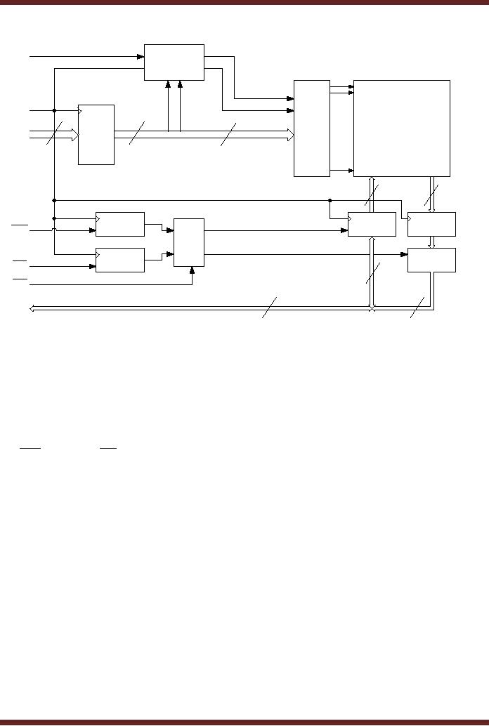
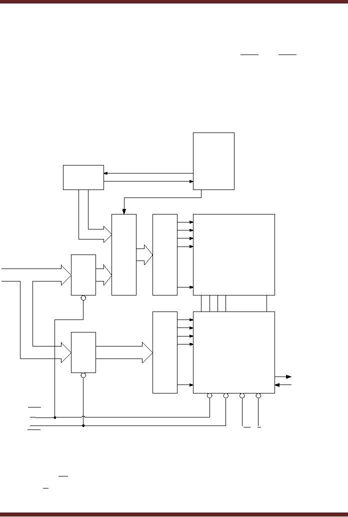
Synchronous
Burst SRAM
RAM chips
are subdivided into
Asynchronous RAM (ASRAM) and
Synchronous Burst
RAM (SB
SRAM).The Static memory
described is an Asynchronous SRAM,
the operation of
which
does not depend upon
the clock signal. The
read and write operations
are carried out
asynchronously.
Synchronous SRAM uses a clock
signal which is used by the
microprocessor
to synchronize
its activities to synchronize
the read and write
operations for faster
operation.
The
block diagram of a Synchronous
Burst SRAM is shown. Figure
40.5.
405
CS302 -
Digital Logic & Design
BURST
A0'
CONTROL
Burst
Logic
A1'
A0
A1
CLK
Address
Decoder
16K x
8
(row
Address
Memory
Array
&
Register
column)
14
14
12
A0-A13
External
Address
8
8
Write
Data
Input
Data
Output
Register
Register
Register
WE
Data
I/O
Control
Enable
Output
Register
Buffers
CS
OE
8
I/O0-I/O7
8
8
Data
Input/Output
Figure
40.5
Block
diagram of a Synchronous Burst
RAM
Synchronous RAM
is very similar to the
Asynchronous RAM, in terms of
the memory
array,
the address decoders,
read/write and enable
inputs. In the Asynchronous
memory the
various
input signals are
asynchronous and are not
tied to the clock, whereas
in the
Synchronous
memory all the inputs
are synchronized with
respect to the clock and
are latched
into
their various registers on an
active clock pulse edge. In
the diagram, the external
address,
the WE and the CS external signals are
latched in on a positive clock
transition
simultaneously.
The data that is to be
written into the memory is
also latched into the
Data
Input
Register at the same
positive clock transition.
For a read operation the
data is latched in
the
Data Output register on the
positive clock transition.
There are two variations of
the
Synchronous
SRAM, the Flow-through and
the Pipelined SRAM. In the
Flow-through SRAM
there is no
Data Output Register so the
data is asynchronously available on
the data lines
during a
read operation. In the
Pipelined version there is a
Data Output Register which
latches
in the
data read from the
memory array.
The
Synchronous SRAM also has a
Burst feature which allows
the Synchronous
SRAM to read or
write up to four locations
using a single address. When
an external address
is latched in by
the Address register, the
lower two bits of the
address are connected to
the
Burst
logic circuitry which
internally increments the
addresses at each clock
transition
producing
four different addresses 00,
01, 10 and 11. For
example, if an external
base
address of
37A0 H is stored in the
Address Register, the Burst
Logic circuitry
produces
addresses
37A0, 37A1, 37A2 and
37A3. The detailed Burst
Logic circuit is shown.
Figure 40.6.
406
CS302 -
Digital Logic & Design
Figure
40.6
Burst
Logic Circuit
Dynamic
RAM
A static RAM
uses a latch to store a
single bit of information.
Four gates are used
to
implement a
latch. In terms of transistors, 4 to 6
transistors are required to
implement a single
storage
cell. In order to build
memories with higher
densities, a single transistor is
used to
store a
binary value. A single
transistor can not store a
binary value however it is
used to
charge
and discharge a capacitor. A
single memory cell is thus
implemented using a
single
transistor
and a capacitor which occupy
lesser space as compared to
the six transistors
which
are
used to implement a single
Static RAM cell. Thus the
density of the capacitor
based
memory is
significantly increased. The
capacitor based memory is
known as a Dynamic RAM
(DRAM).
The drawback of DRAM is the
discharging of the capacitor
over a period of
time.
Unless
the capacitor is periodically
recharged all the
information stored in terms of
binary bits
in a capacitor
based memory array is lost.
The extra circuitry required
to refresh the
capacitor
complicates
the operation of the
DRAM.
The
circuit diagram of a single DRAM
capacitor based memory cell
is shown.
Fig
40.7a.
The capacitor is connected
through a MOSFET which
connects or disconnects
the
column
line at B to the capacitor at D. If
the row is set at logic
high the MOSFET
connects
the
column
line to the capacitor. If
the row line is set to
logic low the MOSFET
disconnects
the
column
line form the
capacitor.
407
CS302 -
Digital Logic & Design
Column
Refresh
Buffer
C
Refresh
Row
Output
Buffer/
B
D
Sense
Amplifier
MOSFET
Capacitor
DOUT
A
R/W
DIN
Bit
line
Input
Buffer
Figure
40.7a Writing a 1 or 0 into
the DRAM cell
A write
operation allows a logic 1 or 0 to be
stored in a DRAM cell (capacitor).
The
appropriate
cell is selected by specifying
the address of the memory
location which is
decoded
and
the row connecting the
desired cell is activated.
The R / W
signal is
set to logic low
indicating a
write operation which
enables the tri-state Input
Buffer. The logic 1 which is
to be
stored in
the memory cell is applied
at the DIN
data
line which is available at A on
the column
line.
The row line is selected
(set to logic high) which
allows the MOSFET to connect
column B
to capacitor D.
The capacitor is charged to
logic 1 voltage level via
ABD. Figure 40.7a. A
Write
operation to
store logic 0 in a DRAM cell is
similar. The appropriate row
is selected by
specifying
the storage location
address. The R / W signal is set to logic
low which enables
the
Input
Buffer. The logic 0 to be
stored in the DRAM cell is
applied at the DIN which is stored on
the
capacitor via ABD. Figure
40.7a. The thick line in
the diagram indicates the
data path from
DIN to the storage
capacitor.
The
read operation is accomplished by
specifying the address of
the location from
which
data is to be read. The DRAM
address decoder activates
the appropriate row.
The
R / W signal is set to
logic high which enables
the output buffer. The
logic 1 or 0 stored on
the
capacitor is
available at DOUT through path DBA.
Figure 40.7b.
The
capacitor can not retain
the charge, therefore it has
to be periodically charged
through a
refresh cycle. The Refresh
Buffer is enabled by setting
the Refresh signal to
high.
The
input of the Refresh Buffer
is connected to the output
buffer/sense amplifier. The R / W
signal is
set to logic high during
the Refresh cycle allowing
the information stored on
the
capacitor to be
available at the output of
the Output Buffer/Sense
amplifier. The information
is
feed
back to the capacitor
through the Refresh Buffer
via path CBD. Figure
40.7c.
408

CS302 -
Digital Logic & Design
Column
Refresh
Buffer
C
Refresh
Row
Output
Buffer/
B
D
Sense
Amplifier
MOSFET
Capacitor
DOUT
A
R/W
DIN
Bit
line
Input
Buffer
Figure
40.7b Reading a 0 or 1 from
the DRAM cell
R/W
Figure
40.7c Refreshing a DRAM
cell
Address
Multiplexing
DRAM chips
use address multiplexing to
reduce the number of address
lines by half.
The
address required to select a
memory location is split
into row and column
addresses. To
409
CS302 -
Digital Logic & Design
access a DRAM
location for reading or
writing of information the
row address is first applied
at
the
address lines. The row
address is latched by the
Row Address Latch of the
DRAM
memory
chip. The column address is
applied next at the same
address lines. The
column
address is
latched by the Column
Address Latch. Two signals
RAS and CAS are used
as
strobe
signals to control the Row
Address and Column Address
latches respectively.
The
external
address lines are
multiplexed as the same set
of address lines are used to
apply the
row
address and the column
address at different time
instances. The outputs of
the Row
Address
Latch and the Column
Address Latch are connected
to the Row and
Column
Decoders
which select a single row
and column line selecting
the storage cell to be
accessed.
Figure
40.8
Refresh
Control
and
Refresh
Timing
Counter
Row
Decoder
Address
Memory
Array
Lines
1024
rows x
A0-A9
1024
columns
Row
Address
Data
Latch
Selector
Input/Output
Buffers
and
Sense
Amplifiers
Column
DOUT
Address
Latch
DIN
Column
Decoder
RAS
R/W
E
CAS
Figure
40.8
Circuit
Diagram of a 1M x 1 DRAM
The R / W signal controls the
Reading and Writing of data
through the DOUT and DIN
lines.
The E
signal
enables the DRAM chip. The
refresh cycle is controlled by
the Refresh
Control
and Timing circuit which
configures the Data Selector
to select row
addresses
410

CS302 -
Digital Logic & Design
generated by
the refresh counter. During
the refresh cycle all
memory cells connected to
the
selected
row are refreshed
simultaneously. Therefore, a 1M bit DRAM
arranged as 1024 rows
and
1024 columns is refreshed by
selecting all the 1024
rows in a sequence.
411
Table of Contents:
- AN OVERVIEW & NUMBER SYSTEMS
- Binary to Decimal to Binary conversion, Binary Arithmetic, 1s & 2s complement
- Range of Numbers and Overflow, Floating-Point, Hexadecimal Numbers
- Octal Numbers, Octal to Binary Decimal to Octal Conversion
- LOGIC GATES: AND Gate, OR Gate, NOT Gate, NAND Gate
- AND OR NAND XOR XNOR Gate Implementation and Applications
- DC Supply Voltage, TTL Logic Levels, Noise Margin, Power Dissipation
- Boolean Addition, Multiplication, Commutative Law, Associative Law, Distributive Law, Demorgans Theorems
- Simplification of Boolean Expression, Standard POS form, Minterms and Maxterms
- KARNAUGH MAP, Mapping a non-standard SOP Expression
- Converting between POS and SOP using the K-map
- COMPARATOR: Quine-McCluskey Simplification Method
- ODD-PRIME NUMBER DETECTOR, Combinational Circuit Implementation
- IMPLEMENTATION OF AN ODD-PARITY GENERATOR CIRCUIT
- BCD ADDER: 2-digit BCD Adder, A 4-bit Adder Subtracter Unit
- 16-BIT ALU, MSI 4-bit Comparator, Decoders
- BCD to 7-Segment Decoder, Decimal-to-BCD Encoder
- 2-INPUT 4-BIT MULTIPLEXER, 8, 16-Input Multiplexer, Logic Function Generator
- Applications of Demultiplexer, PROM, PLA, PAL, GAL
- OLMC Combinational Mode, Tri-State Buffers, The GAL16V8, Introduction to ABEL
- OLMC for GAL16V8, Tri-state Buffer and OLMC output pin
- Implementation of Quad MUX, Latches and Flip-Flops
- APPLICATION OF S-R LATCH, Edge-Triggered D Flip-Flop, J-K Flip-flop
- Data Storage using D-flip-flop, Synchronizing Asynchronous inputs using D flip-flop
- Dual Positive-Edge triggered D flip-flop, J-K flip-flop, Master-Slave Flip-Flops
- THE 555 TIMER: Race Conditions, Asynchronous, Ripple Counters
- Down Counter with truncated sequence, 4-bit Synchronous Decade Counter
- Mod-n Synchronous Counter, Cascading Counters, Up-Down Counter
- Integrated Circuit Up Down Decade Counter Design and Applications
- DIGITAL CLOCK: Clocked Synchronous State Machines
- NEXT-STATE TABLE: Flip-flop Transition Table, Karnaugh Maps
- D FLIP-FLOP BASED IMPLEMENTATION
- Moore Machine State Diagram, Mealy Machine State Diagram, Karnaugh Maps
- SHIFT REGISTERS: Serial In/Shift Left,Right/Serial Out Operation
- APPLICATIONS OF SHIFT REGISTERS: Serial-to-Parallel Converter
- Elevator Control System: Elevator State Diagram, State Table, Input and Output Signals, Input Latches
- Traffic Signal Control System: Switching of Traffic Lights, Inputs and Outputs, State Machine
- Traffic Signal Control System: EQUATION DEFINITION
- Memory Organization, Capacity, Density, Signals and Basic Operations, Read, Write, Address, data Signals
- Memory Read, Write Cycle, Synchronous Burst SRAM, Dynamic RAM
- Burst, Distributed Refresh, Types of DRAMs, ROM Read-Only Memory, Mask ROM
- First In-First Out (FIFO) Memory
- LAST IN-FIRST OUT (LIFO) MEMORY
- THE LOGIC BLOCK: Analogue to Digital Conversion, Logic Element, Look-Up Table
- SUCCESSIVE APPROXIMATION ANALOGUE TO DIGITAL CONVERTER