 |
LOGIC GATES: AND Gate, OR Gate, NOT Gate, NAND Gate |
| << Octal Numbers, Octal to Binary Decimal to Octal Conversion |
| AND OR NAND XOR XNOR Gate Implementation and Applications >> |
CS302 -
Digital Logic & Design
Lesson
No. 05
LOGIC
GATES
The
Digital Systems should be
able to process or perform
operations on the
numbers
that
are represented in the
Binary Number System. The
simplest operations that
come to mind
are
the arithmetic operations
like add and subtract.
There are many more
operations and
functions
that Digital Systems are
able to perform.
Digital
Logic Gates provide the
basic building blocks; these
Logic Gates perform
different
operations on the Binary
information. These Logic
Gates are used in
different
combinations to
implement large complex
systems. Digital Logic Gates
are represented and
identified by
unique symbols. These
symbols are used in circuit
diagrams to describe
the
function of a
digital circuit.
Digital
Logic Gates function is
represented by a function table or a
truth table that
describes
all the Logic gate
outputs for every possible
combination of inputs. As the
logic
Gates
operate on binary values
therefore these function
tables describes the
relationship
between
the input and output in
terms of binary values. The
function of a Logic Gate is
also
described in
terms of an expression.
Logic
Gates are practically used
in circuits where the inputs
to the Logic Gates vary
in
time.
Timing diagrams are used to
describe the response of the
Logic Gates in a certain
period
of time
with respect to the changing
input. Timing diagrams
graphically show the
actual
performance
(behavior) of the logic gate
to the changing inputs for a
predetermined period of
time or
sequence of input
signals.
The
three fundamental Gates are
the AND, OR and NOT
Gates.
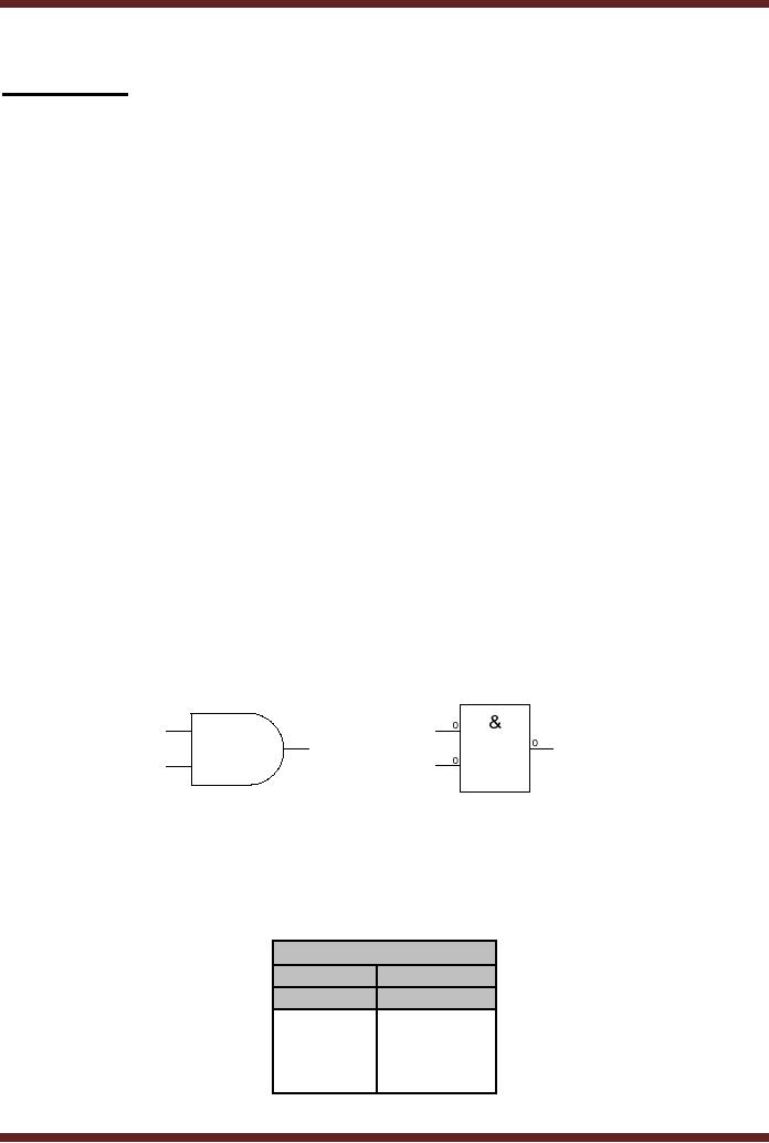
AND
Gate
The AND
Gate performs a logical
multiplication function. An AND Gate
has multiple
inputs
and a single output. Most
commonly used AND Gates are
two input AND gates.
An
AND Gate is
represented by the symbols
shown in Figure 5.1
Figure
5.1
Symbolic
representation of AND Gate
The
multiplication function performed by
the AND Gate is shown in the
function table
for a
two input AND Gate. Figure
5.2. The function table
for a 3, 4 or multiple input AND
Gate
is similar.
The output is 1 when all
the inputs are at logic
level 1. For all other
input
combinations
the output is zero.
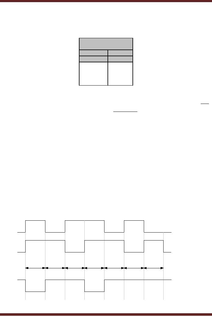
Logical AND
Operation
Inputs
Output
A
B
F
0
0
0
0
1
0
1
0
0
1
1
1
Figure
5.2
Function
Table of an AND Gate
40

CS302 -
Digital Logic & Design
The
expression describing the
operation of a two inputs AND
Gate is F
=
A.B
The `.' is an
AND Operator and the
expression represents an AND operation
between inputs A
and B.
Expression for multiple
input AND Gates is F = A.B.C. ⋅ ⋅ ⋅ N , where N is the
total
number of
inputs.
The
timing diagram of the two
input AND gate with the
input varying over a period
of 7
time
intervals is shown in the
diagram. Figure 5.3.
Figure
5.3
Timing
diagram of operation of an AND
gate
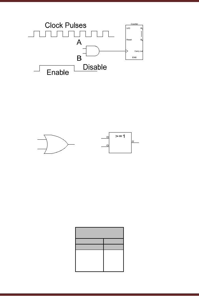
An important
use of an AND gate in addition to
the multiplication operation is
its use to
disable or
enable a device. Figure 5.4.
A Counter device counts from
0 to 100. The counter
device
increments its current count
value to the next when it
receives a pulse at its
clock input.
To allow
the Counter device to count
continuously from 0 to 100,
continuous pulses are
applied at
the clock input of the
Counter Device. The
continuous pulses are shown
as Clock
pulses.
The
counter can be stopped from
counting by stopping the
clock pulses from
reaching
the
clock input of the Counter
Device. A 2-input AND gate is
connected to the Counter
Clock
input.
The clock pulses are
applied at the Input A of
the AND Gate. Input B of the
AND Gate is
connected to an
Enable/Disable signal. When
the Counter Device is
stopped from counting
the
enable/disable
signal ay Input B is set to
0.
The
Function Table, figure 5.2,
indicates that when ever an
input of the AND gate is
set
to 0 the
output also becomes 0. Thus
by applying the disable
signal 0 at Input B, the
output of
the
gate becomes zero and
therefore clock signals are
prevented from reaching the
Counter
device. To
allow the Counter Device to
count, the enable/disable
signal at input B of the
AND
gate is
set to 1. The Function Table
of the AND gate indicates
that when an Input of the
AND
gate is 1,
the output follows the
input signal applied at the
input A of the AND Gate.
Thus the
clock
signal at Output of the AND
gate follows the clock
signal at Input A of the AND
Gate.
41
CS302 -
Digital Logic & Design
Figure
5.4
Enabling a
Counter using an AND
Gate
OR
Gate
The OR
Gate performs a Boolean add
function. An OR Gate has
multiple inputs and a
single
output. Most commonly used
OR Gates are two input OR
gates. An OR Gate is
represented by
symbols as shown in figure
5.5.
Figure
5.5
Symbolic
representation of OR Gate
The
addition function performed by
the OR Gate is shown in the
function table for a
two
input OR
Gate. Figure 5.6. The
function table for a 3, 4 or
multiple input OR Gate is
similar.
The
output is 1 when any one
input is at logic level 1.
The output is 0 when all
inputs are zero.
The
expression describing the
operation of the two inputs
OR Gate is F
=
A + B . The
`+' is an OR
Operator and the expression
represents an OR operation between
inputs A and B.
Expression
for multiple input OR Gates
is F = A + B + C + .....N , where N is the
total number of
inputs.
Logical
OR
Operation
Inputs
Output
A
B
F
0
0
0
1
0
1
1
1
0
1
1
1
Figure
5.6
Function
Table of an OR Gate
42
CS302 -
Digital Logic & Design
The
timing diagram of the two
input OR gate with the
input varying over a period
of 7
time
intervals is shown in the
diagram 5.7.
A
B
t0
t1
t2
t3
t4
t5
t6
F
Figure
5.7
Timing
diagram of operation of an OR
gate
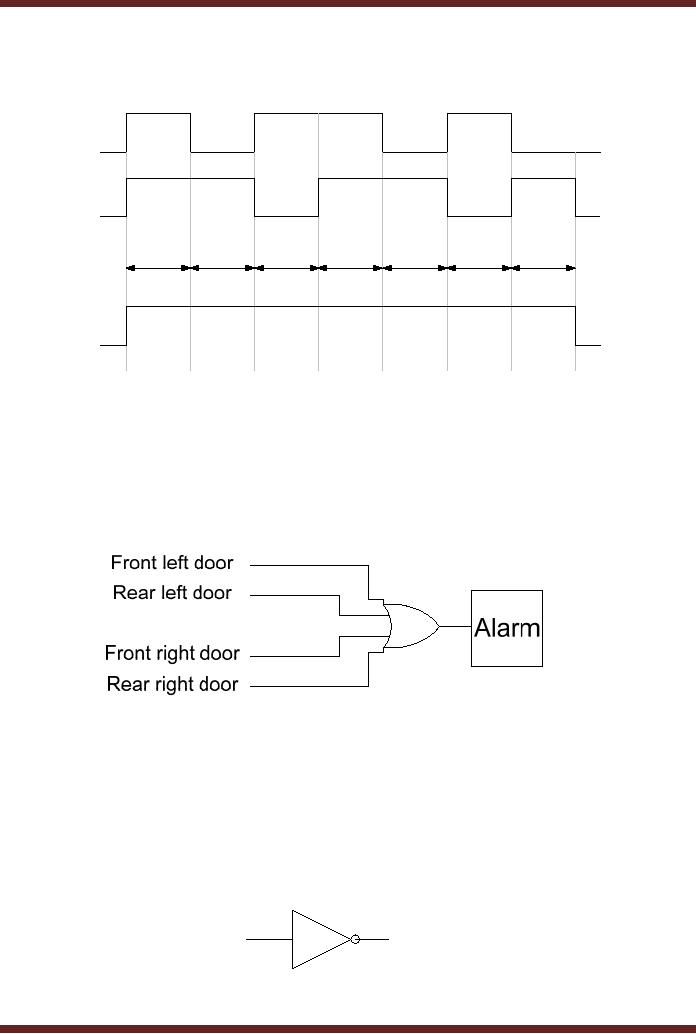
The OR
Gate is used in applications
where the output signal is a
1 when any one
input
is a 1. An
example of such an application is an
alarm circuit for car
door locks shown in
diagram,
figure 5.8. Four circuits
are connected to each of the
four doors of a car. The
door
circuit
generates a 1 when the door
is open and a 0 when it is
closed. The four outputs of
each
of the
four door circuits are
connected to the four inputs
of an OR Gate. The output of
the OR
gate is
connected to an Alarm.
Figure
5.8
Car
door Alarm System based on a
4-input OR Gate
When
any one or more doors
are open the inputs of
the OR Gate have a 1. The
output
of the OR
gate is a 1, according to the
Function Table of an OR Gate,
figure 5.6, which
enables
the Alarm.
NOT
Gate
NOT
Gate is also known as an
Inverter. The name indicates
that the NOT Gate
should
be performing an
inversion function. The Not
Gate has a single input
and a single output.
The
NOT
Gate is represented by the
symbol shown in Figure
5.9.
Figure
5.9
NOT
Gate
43
CS302 -
Digital Logic & Design
The
input signal applied across
the single input of the OR
gate is inverted and
is
available at
the output. The function of
the NOT Gates is described
by the Function Table
or
the
Truth Table represented in
Figure 5.10.
Logical
NOT
Operation
Input
Output
A
F
0
1
1
0
Figure
5.10
Function
Table of a NOT Gate
The
expression describing the
behavior of a NOT gate in
terms of the Input and
Output
shown in
the Function Table, Figure
5.10 is F
=
A where A indicates invert of A
The
timing diagram of a NOT gate
with the input varying
over a period of 7
time
intervals
and its corresponding output
is shown in the Figure
5.11.
Figure
5.11
Timing
diagram of operation of a NOT
gate
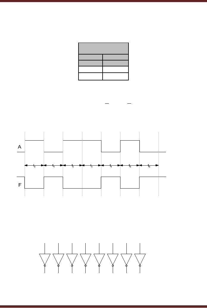
The
NOT Gate is used in circuits
to generate the 1's
Complement of a number by
inverting
all its bits. Figure
5.12. It is also used to
invert an incoming signal
`1' as per
requirements of
another circuit which
requires the signal to be
`0'.
1
0
0
1
1
0
1
0
0
0
1
1
0
1
0
1
Figure
5.12
A 1's
Complement Circuit using 8
NOT Gates
44

CS302 -
Digital Logic & Design
In addition to
the three Fundamental Gates
which perform AND, OR and
NOT operations, two
other
important gates that are
commonly used in Digital
Logic are the NAND and
NOR Gates.
These
two gates do not perform
any new functions. The NAND
Gate performs an
AND-NOT
function
and the NOR gate
performs the OR-NOT
function.
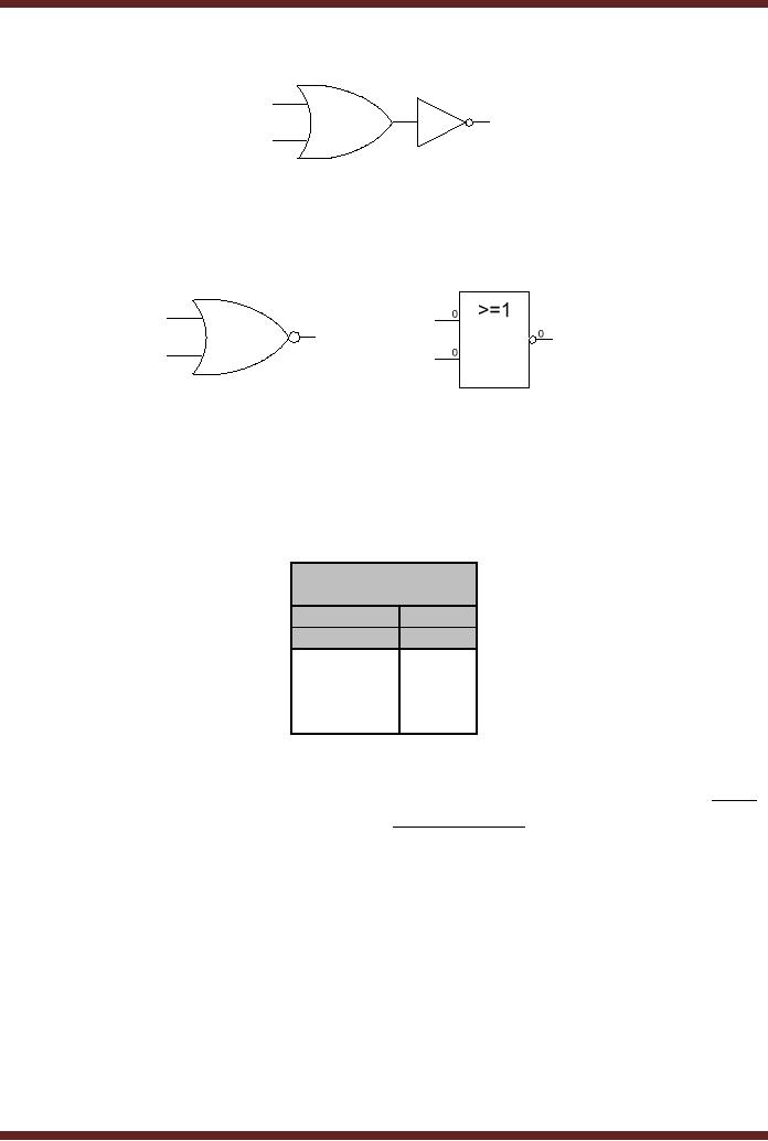
AND & OR Gate
alternate symbols
The AND
gate and the OR gate
can also be represented by
alternate symbols. The
two
fundamental
symbols, the AND Gate symbol
and the OR gate symbol
complement each
other.
Thus a
gate can be represented by
its complementary symbol.
The inputs and outputs of
the
complementary
symbol are inverted by
placing or removing bubbles.
Figure 5.13.
Figure
5.13
Alternate
Symbolic representation of AND & OR
gates
The AND
gate is represented by its
complementary OR gate symbol,
the two inputs
and
the output are inverted by
placing bubbles. The OR gate
is represented by its
complementary
AND gate symbol, the two
inputs and the output
are inverted by
placing
bubbles.
NAND
Gate
The NAND
Gate performs a function
that is equivalent to the
function performed by
the
combination of
an AND gate and a NOT gate.
Figure 5.14
A NAND Gate
has multiple inputs and a
single output. Most commonly
used NAND
Gates
are two input NAND gates. A
NAND gate is represented by the
symbols shown in
figure
5.15,
the NOT gate connected at
the output of the AND gate
is represented by a circle, in
Digital
Logic terminology a
`bubble'.
Figure
5.14
NAND Gate
function
Figure
5.15
Symbolic
representation of NAND Gate
The
function performed by the NAND
Gate is described by the
Function Table for a
two
input NAND
Gate. Figure 5.16. The
function table for a 3, 4 or
multiple input NAND Gate
is
45
CS302 -
Digital Logic & Design
similar.
The output is 0 when all
inputs are 1s. For
all other combinations of
inputs the output
logic
level is 1.
Logical
NAND
Operation
Inputs
Output
A
B
F
0
0
1
0
1
1
1
0
1
1
1
0
Figure
5.16
Function
Table of a NAND Gate
The
expression describing the
operation of the two inputs
NAND Gate is F
=
A.B .
Expression
for multiple input NAND
Gates is F
=
A.B.C......N , where N is the
total number of
inputs.
The
timing diagram of the two
input NAND gate with the
input varying over a period
of
7 time
intervals is shown in the
diagram. Figure 5.17.
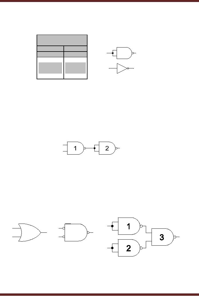
NAND
Gate as a Universal
Gate
The NAND
gate is also used as a
Universal Gate as the NAND
Gate can be used in a
combination to
perform the function of a
AND, OR and NOT
gates.
1. NOT
Gate Implementation
A NOT
gate can be implemented
using a NAND gate by connecting
both the inputs of
the
NAND gate
together. By connecting the
two inputs together, the
input combinations where
the
inputs
are dissimilar become
redundant. The Function
Table of the 2-input NAND
Gate
reduces to
that of the NOT gate.
Figure 5.18
A
B
t0
t1
t2
t3
t4
t5
t6
F
Figure
5.17
Timing
diagram of operation of a NAND
gate
46
CS302 -
Digital Logic & Design
Logical
NAND
Operation
Inputs
Output
A
B
F
0
0
1
0
1
1
1
0
1
1
1
0
Figure
5.18
Implementing a
NOT Gate using a NAND
gate
2. AND Gate
Implementation
A NAND Gate
performs the AND-NOT
function. Removing the NOT
gate at the output
of the NAND
gate results in an AND gate.
The effect of the NOT
gate at the output of
the
NAND gate
can be cancelled by connecting a
NOT gate at the output of
the NAND Gate. The
two
NOT gates cancel each
other out. A NOT Gate
implemented using a NAND gate
(2) is
connected to
the output of a NAND gate
(1). Figure 5.19.
Figure
5.19
Implementing an
AND Gate using two NAND
gates
3. OR Gate
Implementation
An OR Gate
can be implemented using a
combination of three NAND gates.
The
implementation
is based on the alternate
symbolic representation of the OR
gate. The OR
gate is
represented as an AND gate with
bubbles at the inputs and
outputs. Figure 5.13.
The
two
bubbles at the input can be
replaced by two NOT gates
(1) & (2) implemented
using two
NAND gates. If
the two bubbles are
removed from the two
inputs, the AND gate with
the
bubble at
the output represents a NAND
gate (3). Figure
5.20
Figure
5.20
Implementing an
OR Gate using three NAND
gates
NOR
Gate
The
NOR Gate performs a function
that is equivalent to the
function performed by a
combination of
an OR gate and a NOT gate.
Figure 5.21
47
CS302 -
Digital Logic & Design
Figure
5.21
NOR
Gate function
A NOR
Gate has multiple inputs
and a single output. Most
commonly used NOR
Gates
are
two input NOR gates. A
NOR gate is represented by
the symbols shown in figure
5.22, the
NOT
gate connected at the output
of the OR gate is represented by a
circle.
Figure
5.22
Symbolic
representation of NOR
Gate
The
function performed by the
NOR Gate is described by the
Function Table for a
two
input
NOR Gate. Figure 5.23.
The function table for a 3,
4 or multiple input NOR Gate
is
similar.
The output is 1 when all
inputs are 0s. For
all other combinations of
inputs the output
logic
level is 0.
Logical
NOR
Operation
Inputs
Output
A
B
F
0
0
1
0
1
0
1
0
0
1
1
0
Figure
5.23
Function
Table of a NOR Gate
The
expression describing the
operation of the two inputs
NOR Gate is F = A + B .
Expression
for multiple input NOR
Gates is F
=
A + B + C + .....N , where N is the
total number
of
inputs.
The
timing diagram of the two
input NOR gate with
the input varying over a
period of 7
time
intervals is shown in the
diagram. Figure 5.24.
48
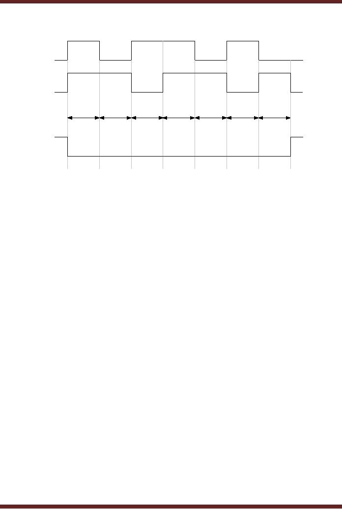
CS302 -
Digital Logic & Design
A
B
t0
t1
t2
t3
t4
t5
t6
F
Figure
5.24
Timing
diagram of operation of a NOR
gate
49
Table of Contents:
- AN OVERVIEW & NUMBER SYSTEMS
- Binary to Decimal to Binary conversion, Binary Arithmetic, 1s & 2s complement
- Range of Numbers and Overflow, Floating-Point, Hexadecimal Numbers
- Octal Numbers, Octal to Binary Decimal to Octal Conversion
- LOGIC GATES: AND Gate, OR Gate, NOT Gate, NAND Gate
- AND OR NAND XOR XNOR Gate Implementation and Applications
- DC Supply Voltage, TTL Logic Levels, Noise Margin, Power Dissipation
- Boolean Addition, Multiplication, Commutative Law, Associative Law, Distributive Law, Demorgans Theorems
- Simplification of Boolean Expression, Standard POS form, Minterms and Maxterms
- KARNAUGH MAP, Mapping a non-standard SOP Expression
- Converting between POS and SOP using the K-map
- COMPARATOR: Quine-McCluskey Simplification Method
- ODD-PRIME NUMBER DETECTOR, Combinational Circuit Implementation
- IMPLEMENTATION OF AN ODD-PARITY GENERATOR CIRCUIT
- BCD ADDER: 2-digit BCD Adder, A 4-bit Adder Subtracter Unit
- 16-BIT ALU, MSI 4-bit Comparator, Decoders
- BCD to 7-Segment Decoder, Decimal-to-BCD Encoder
- 2-INPUT 4-BIT MULTIPLEXER, 8, 16-Input Multiplexer, Logic Function Generator
- Applications of Demultiplexer, PROM, PLA, PAL, GAL
- OLMC Combinational Mode, Tri-State Buffers, The GAL16V8, Introduction to ABEL
- OLMC for GAL16V8, Tri-state Buffer and OLMC output pin
- Implementation of Quad MUX, Latches and Flip-Flops
- APPLICATION OF S-R LATCH, Edge-Triggered D Flip-Flop, J-K Flip-flop
- Data Storage using D-flip-flop, Synchronizing Asynchronous inputs using D flip-flop
- Dual Positive-Edge triggered D flip-flop, J-K flip-flop, Master-Slave Flip-Flops
- THE 555 TIMER: Race Conditions, Asynchronous, Ripple Counters
- Down Counter with truncated sequence, 4-bit Synchronous Decade Counter
- Mod-n Synchronous Counter, Cascading Counters, Up-Down Counter
- Integrated Circuit Up Down Decade Counter Design and Applications
- DIGITAL CLOCK: Clocked Synchronous State Machines
- NEXT-STATE TABLE: Flip-flop Transition Table, Karnaugh Maps
- D FLIP-FLOP BASED IMPLEMENTATION
- Moore Machine State Diagram, Mealy Machine State Diagram, Karnaugh Maps
- SHIFT REGISTERS: Serial In/Shift Left,Right/Serial Out Operation
- APPLICATIONS OF SHIFT REGISTERS: Serial-to-Parallel Converter
- Elevator Control System: Elevator State Diagram, State Table, Input and Output Signals, Input Latches
- Traffic Signal Control System: Switching of Traffic Lights, Inputs and Outputs, State Machine
- Traffic Signal Control System: EQUATION DEFINITION
- Memory Organization, Capacity, Density, Signals and Basic Operations, Read, Write, Address, data Signals
- Memory Read, Write Cycle, Synchronous Burst SRAM, Dynamic RAM
- Burst, Distributed Refresh, Types of DRAMs, ROM Read-Only Memory, Mask ROM
- First In-First Out (FIFO) Memory
- LAST IN-FIRST OUT (LIFO) MEMORY
- THE LOGIC BLOCK: Analogue to Digital Conversion, Logic Element, Look-Up Table
- SUCCESSIVE APPROXIMATION ANALOGUE TO DIGITAL CONVERTER