 |
LAST IN-FIRST OUT (LIFO) MEMORY |
| << First In-First Out (FIFO) Memory |
| THE LOGIC BLOCK: Analogue to Digital Conversion, Logic Element, Look-Up Table >> |
CS302 -
Digital Logic & Design
Lesson
No. 43
LAST
IN-FIRST OUT (LIFO)
MEMORY
Last
In-First Out Memory finds
applications in computer systems
where it is used to
implement a
stack. The operation of a
stack can be understood by
viewing a stack of plates.
In
a stack of
plates the first plate is
placed at the bottom the
next plate placed is placed
on the
top,
the third plate is placed on
the top of the second
plate and so on. Plates
are removed one
at a time
from the top of the
stack, thus the last
plate placed on the stack
top is the first to
be
removed
followed by the second plate
and then the plate at
the bottom which was
placed first.
In a register
based LIFO memory
implementation a set of Parallel
In/Parallel Out registers
are
connected
together such that data is
pushed down or pulled up
when data is stored
or
removed
from the memory
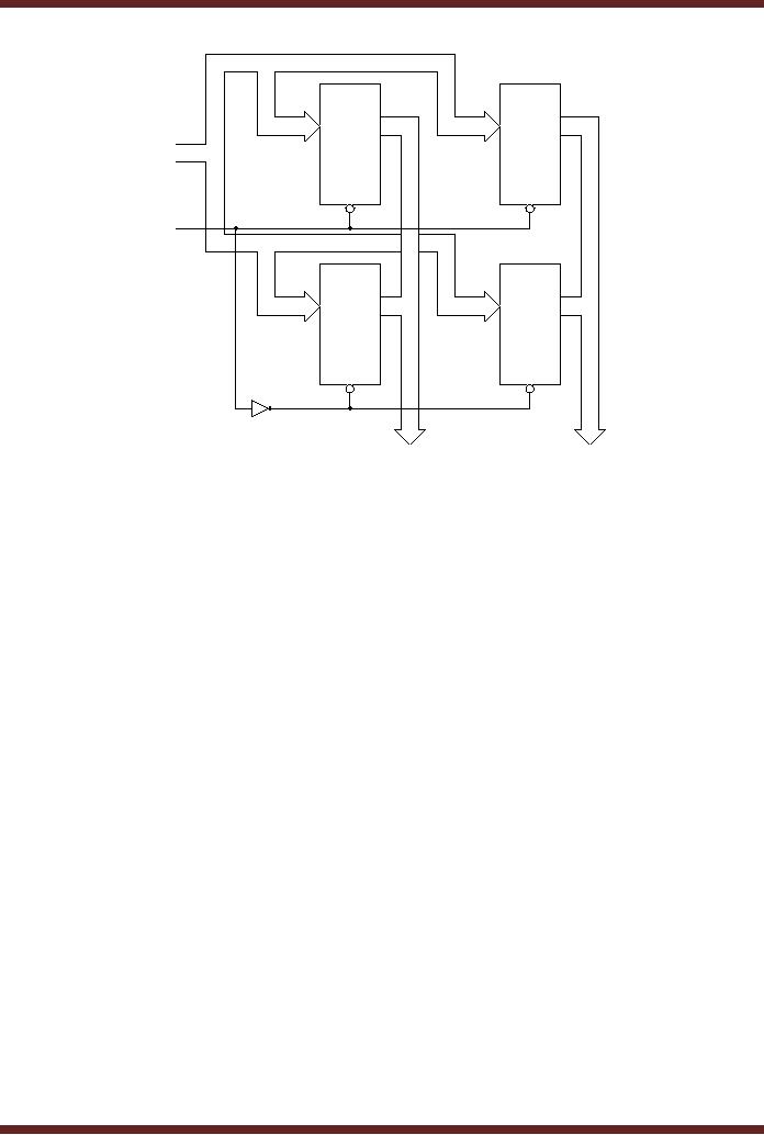
respectively. Figure
43.1.
Stack
Top
Register
1
Register
2
Stack
Register
3
Control
Register
4
Register
5
Figure
43.1
A five
byte LIFO Memory
In the
LIFO memory shown, the
first 8-bit data value is
stored in the first register
Reg.
1. To store
the next value, the
first value stored in Reg. 1
is pushed down (shifted) to
the
second
register Reg. 2. The second
8-bit data value is written
into the first register
Reg. 1. The
third
data value can only be
stored when both the
previous values are pushed
(shifted) down
to the
Registers 2 and 3. A maximum of
five, 8-bit data values
can be stored in the
LIFO
register.
The fifth and the
last value stored in the
first register Reg. 1 is the
first value to be
read
out. The remaining four
values in the memory are
pulled (shifted) up. At any
time new
data
can be added to the LIFO
memory or the stored data
can be read out.
Shift
Register based Stack
implementation finds use in
specialized digital systems.
A
practical
way to implement the program
stack which a program under
execution uses to
access
variables is by means of the RAM
memory. The stack is known
as a RAM Stack. A
special
purpose register known as
the `Stack Pointer Register'
stores the address of the
top of
the
stack, a reserved area in
the RAM memory. As data
values are written or read
from the
RAM stack,
the Stack Pointer Register
increments or decrements its
contents always
pointing
to the
stack top. Figure
43.2.
429
CS302 -
Digital Logic & Design
Initially,
the Stack Pointer Register
has the contents 0, which is
address of memory
location of
the stack. A value `7' is
stored in the Stack by
writing it to memory location
0
pointed to by
the Stack Pointer Register.
To store the next value 4 in
the stack the contents
of
the
Stack Register are
incremented so that the next
vacant location in the Stack
is accessed.
The
new data value 4 is written
at the new location.
Similarly, data values 9 and
8 are stored in
the
next two consecutive
locations in the Stack. The
Stack Pointer Register
points to the Stack
Top
(location 3) which has the
data value 8 stored. A data
value can be read from
the Stack
Top by
reading the data value
from the address pointed to
by the Stack Pointer
Register. After
reading
the data value the
contents of the Stack
Pointer Register are
decremented to point to
the
new Stack Top.
Locations
3
4
Stack
8
3
Pointer
Register
2
9
1
4
7
0
Figure
43.2
Memory
Based Stack
Memory
Expansion
Digital
systems require different
amounts of memory in the
form of RAM and ROM
Memory
depending upon specific
applications. A computer requires
large amounts of RAM
memory to
store multiple application
programs, data and the
operating system. In a
computer,
part of
the RAM is reserved to support
the Video Memory, Stack
and I/O buffers. The
ROM
used by a
computer is relatively very
small as it stores few bytes
of code used to Boot
the
Computer
system on power up.
Micro-controller based digital
system designed for
specific
applications do
not have large memory
requirement, in fact the
total memory requirement
of
such
micro-controller systems is met by
on-board RAM and ROM having a
total storage
capacity of
few hundred of kilobytes.
Computer and Digital systems
have the capability
to
allow RAM
memory to be expanded as the
needed arises by inserting
extra memory in
dedicated
memory sockets on the
computer motherboard.
The
total amount of memory that
is supported by any digital
system depends upon
the
size of
the address bus of the
microprocessor or a micro-controller. A
microprocessor having
an address
bus of 16 bits can generate
216 or 65536 unique
addresses to access
65536
locations
which allows either a single
65536 location RAM or a combination of
RAM and ROM
totalling
65536 memory locations to be
connected to the microprocessor. It is
also possible to
initially
have a 32768 location RAM
connected to the microprocessor
with the remaining
32768
address
locations unoccupied allowing
the microprocessor to execute a
program that can be
stored in
32768 locations. The
remaining memory space can
be utilized latter by
connecting
430

CS302 -
Digital Logic & Design
another
32768 location RAM.
Microprocessors used in computer
systems have memory
spaces of
the order of 232 and
larger.
The
data unit size accessed by a
microprocessor when it issues an
address to either
read or
write from or to a memory
also depends upon the
microprocessor architecture
more
specifically
the number of the data
lines. A microprocessor having an
8-bit data bus
can
access a
byte of information from any
unique memory location. A
microprocessor having a
16-
bit
data bus allows two
bytes to be accessed from a
memory location.
Practically,
microprocessors
used in computer systems
have up to 64 bit wide data
buses allowing up to 8
bytes of
data to be accessed simultaneously. A
microprocessor that accesses
64-bits of data
simultaneously
requires RAM to be organized in such a
way that allows 8 bytes of
data to be
accessed
when ever any unique
address is selected. On the
other hand a
microprocessor
having a
data bus of only 8-bits
requires RAM that allows
only a single byte of data
to be
accessed
when ever any single
address location is
selected.
The
total memory requirement of a
computer or digital system is
determined by the
size of
the address and data
bus of a microprocessor. Microprocessors
which have small
address
bus and a data bus
have a small memory space.
Microprocessors which have
wide
address
and data buses have
very large memory spaces
which are rarely fully
occupied by
RAM and ROM
devices.
Memory,
both RAM and ROM are
implemented in fixed data
unit sizes of 1, 4 or 8
bits.
Similarly,
these memory devices are
implemented having sizes in
terms of total
addressable
locations
which are restricted to
address ranges between few
hundred kilobytes to
megabytes.
The
memories that are available
in fixed sizes have to be
connected together to form
larger
memories
having appropriate data unit
sizes and total number of
addressable locations to
fulfil
the
memory space requirements of a
digital or computer system.
Another important aspect
of
the RAM
and ROM memories that are
manufactured are the
addresses of each
memory
location.
For example, two 32Kbyte RAM
chips have 215 locations each. The
first addressable
locations in
both the RAM chips have an
address 0. Similarly, the
second and third locations
in
both
the memory chips have
addresses 1 and 2 respectively. If
the two RAM chips
are
connected
together to form a 64 Kbyte RAM
then one of 32Kbyte memory
chips should
respond to
the address between 0 and
32767 and the other
32Kbyte memory chip
should
respond to
the address 32768 and
65535. The two memory
chips have bases address 0
and
32768
respectively.
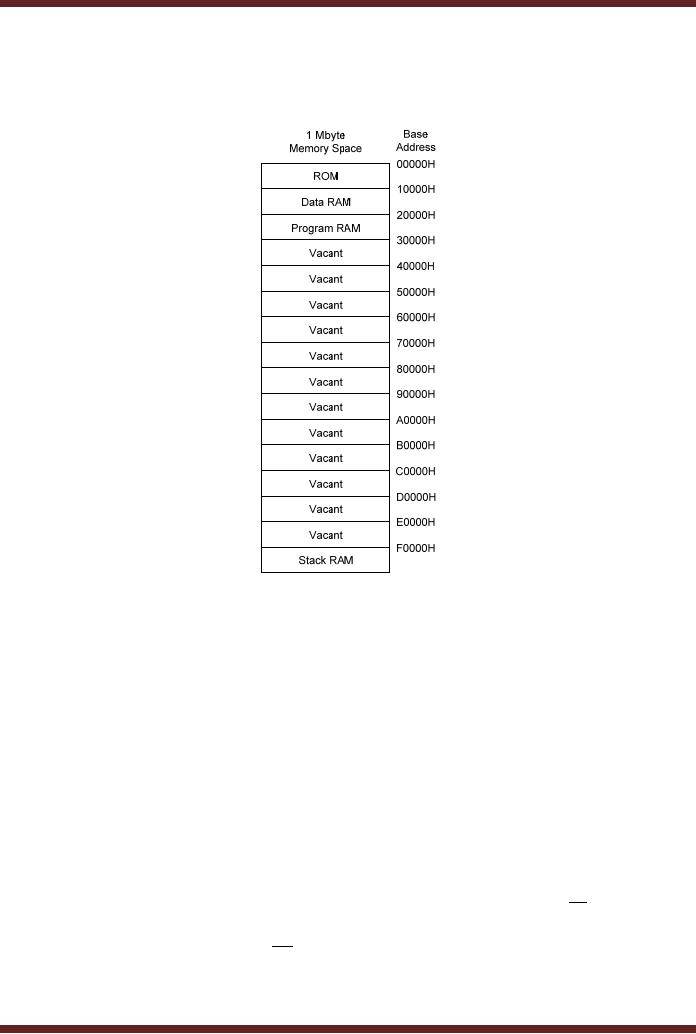
Memory
Map
The
Memory Map of any digital
system specifies the total
memory space that can
be
accessed by
the microprocessor and the
distribution of the total
addressable space
amongst
RAM,
ROM, stack and buffers.
The memory map shown in
the figure shows the
division of 1
MByte of
addressable space into ROM,
RAM for storage of data, RAM
for storage of
program
code,
vacant space which can be
used in the future and a
stack. Figure 43.3. The 1
MByte
address
space is divided into 16
equal blocks of 64 Kbytes
each. The first 64Kbyte
block
having a
base address 00000H is
reserved for ROM memory. A
maximum 64Kbyte sized
ROM chip
can be connected in the
memory space. If a smaller ROM
chip is connected in
the
memory
space, the remaining
unoccupied addresses can be
utilized in future to expand
the
ROM memory by
connecting extra ROM chips.
The next block of 64KByte is
reserved for
storage of
data by connecting a 64KByte RAM
chip. The base address of
the block is 10000H.
The
third block of 64KByte is
used to store program code
by connecting a 64KByte RAM
chip.
The
base address of the third
block is 20000H. The last
64KByte block having a base
address
of F0000H is
reserved for implementing
the stack. A 64Kbyte RAM
chip is connected at
the
431
CS302 -
Digital Logic & Design
base
address F0000H to support
the Stack. Twelve blocks
starting from base address
30000H
are
left unoccupied. These
blocks can be used to
connect additional RAM to increase
the total
amount of
Memory RAM.
Figure
43.3
1 MByte
Memory Map
Expanding
Data Unit Size
Memories
are implemented in 1, 4 and 8
bit data unit sizes. A
processor that
accesses
16-bit of
data at each address
location requires memory to be
connected such that
each
address
location allows access to
16-bits of data. In the
example shown, two 4 K byte
RAM
chips
are connected together to
form a 4K Word (16-bit)
memory or 8K Byte memory.
Figure
43.4. A
4KByte RAM memory chip has
A0 A11 address lines to address 4K
locations. The
address
lines of both the 4KByte RAM
chips are connected together
so that the same
address
is used to
select identical memory
locations in both the memory
chips. Each 4KByte RAM
chip
has 8
data lines to allow access
to 8-bits of data at each
memory location. The address
lines
of both
the memory chips are
kept separate. The memory
chip shown on the right
stores the
least
significant byte of the
16-bit data and the
chip on the left stores
the most significant
byte
of the
16-bit data value. The
least significant byte is
accessed through data lines
D0 D7 and
the
most significant byte is
accessed through data lines
D8 D15. The
R / W control
line of
both
the memory chips are
also connected together so
that a word (16-bit) value
is read or
written to
the selected location. The
CS pins of
both the chips are
also connected together
so
that
both the memory chips
are selected simultaneously
when ever a read or write
memory
operation is
carried out.
432

CS302 -
Digital Logic & Design
Figure
43.4
Implementing 4K
Word RAM using two 4K Byte
RAM chips
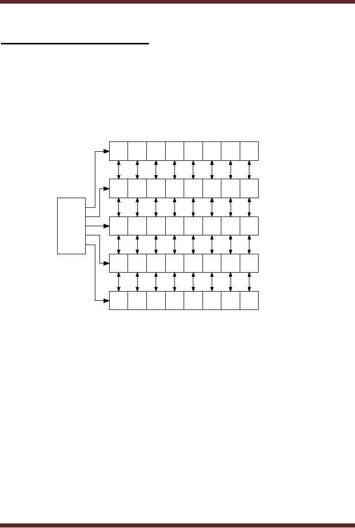
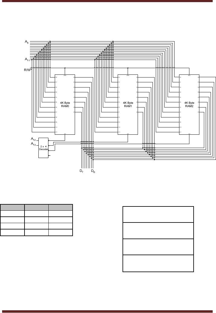
Expanding
Memory Locations
The
two 4KByte memory chips
can be connected together to
form an 8 KByte
memory
thereby
doubling the total number of
memory locations. Addressing
8KByte of memory
requires 13
address lines. The first 12
address lines A0
A11 of the two
memory chips are
connected
together, the data lines of
both the chips are
also connected together.
Since the
data
lines are shared, therefore
at any given instant data
can be read or written to
one of the
two
chips. Selection of either of
the two memory chips is
done through the CS signal. The
first
memory
chip which maps the
address range from 0 to 4K is
selected when the CS signal is
set to
logic 0. The second memory
chip which maps the
memory range 4K to 8K is
connected
to the
CS through a NOT
gate therefore it is selected
when the signal is set to
logic high. The
CS line is connected
to the A12
address
line which selects the
first memory chip when it
is
logic 0,
the second memory chip is
selected when the A12 signal is set to logic 1.
Figure 43.5.
433
CS302 -
Digital Logic & Design
Figure
43.5
Implementing 8K
Byte RAM using two 4K Byte
RAM chips
Expanding
Data Unit Size and
Memory Locations
Memory
chips can be connected
together in different manners to
increase the total
size
(locations) or
the size of the data
unit stored. Four 4K Byte
chips can be connected
together to
implement an 8K
x Word memory. Figure 43.6.
Chips A and B are connected
to provide 4K x
16 bit of
memory space and the
chips C and D are connected
to provide another 4K x 16 bit
of
memory
space. The RAM chips A and B
are selected simultaneously
when A12
address
line is
set to
logic 0. The RAM chips C and
D are selected simultaneously
when A12
address
line is
set to
logic 1. The R / W control
line is connected to all the
four RAM chips. RAM chips A
and
C provide
access to upper byte of the
16-bit data and RAM chips B
and D provide access
to
the
lower byte of the 16-bit
data.
434
CS302 -
Digital Logic & Design
4K x 8
4K x 8
RAM
RAM
A0 - A11
A
B
A12
4K x 8
4K x 8
RAM
RAM
C
D
D8 - D15
D0 - D7
Figure
43.6
An 8K x 16 RAM
implemented using four 4K x 8
memory chips
Address
Decoders
All
memory chips have the
first location identified by
address zero. The next
location
has
the address one and
successive memory locations
have addresses assigned in
an
ascending
order. When these memory
chips are connected to a
microprocessor at the
specified
location represented in the
memory map the memory
chips are connected such
that
the
memory chip has the
start address specified by a
Base Address and the
successive
memory
locations are selected by
ascending addresses with
respect to the Base
address.
Thus
the first memory location is
accessed by the Base Address
and the next
successive
location is
accessed by Base Address +1
and so on. In the 8KByte
memory implemented in
figure
43.5 the first 4KByte
memory has the base
address 0000H and the
second 4KByte
memory
chip has a base address
1000H. A memory chip is
connected at the Base
Address by
selecting it
when the specified Base
Address is generated by the
microprocessor. An Address
Decoder
detects the generated Base
Address and selects the
desired memory chip.
Three
4KByte memory chips are
shown to be connected at Base
Addresses 0000H,
1000H
and 2000H respectively.
Figure 43.7. A 2 x 4 decoder is
used for address
decoding.
The
most significant address
lines A12
and A13 are connected to the
two input lines of the 2 x
4
decoder.
When both the address
lines are logic 0, the
base address is
0000
and the first 4K memory
chip RAM1 is selected. When A12 address line is logic 1
it
indicates
the Base Address 4K which
selects the second 4K memory
chip RAM2. When
address
line A13
is set to
logic 1 it indicates a Base
Address 8K selecting the
third 4K memory
chip
RAM3.
435
CS302 -
Digital Logic & Design
Figure
43.7a Address Decoding of
three 4KByte memory
chips
The
memory map of the memory
configuration shown in figure
43.7a is shown in
figure
43.7b.
A13
A12
Output
0
0
CS0
4K RAM0
0
1
CS1
1
0
CS2
4K RAM1
1
1
CS3
4K RAM2
Vacant
Figure
43.7b Memory Map for the
three 4K RAM chips
Memory
Decoders can be implemented in
different ways. The simplest
method to
implement is by
using logic gates. The
other method is to use m x n
decoders. Both
decoders
are
shown. Figure 43.8 and
43.9. In the logic based
address decoder a combination of
OR,
436
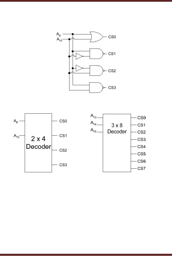
CS302 -
Digital Logic & Design
NAND and
NOT gates are used to
select four memory devices
at Base Addresses
000H,
200H,
400H, 600H respectively. A 2 x 4
Decoder is used to decode
the same memory
space.
A 3 x 8 Decoder
divides the 64K memory
space into eight equal
blocks of 8K.
Figure
43.8
Logic
Gate based Address
Decoder
Figure
43.9
2 x 4 and 3 x 8
Decoder based Address
Decoders
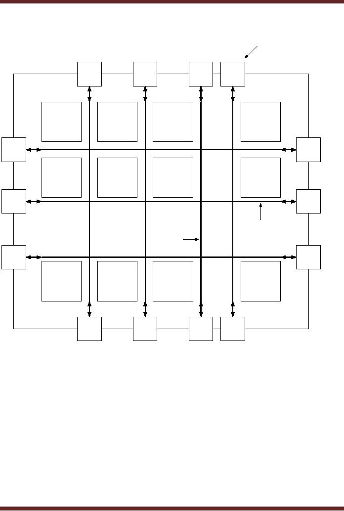
Introduction to
FPGAs
Programmable
Logic Devices are based on a
programmable AND-OR gate
array which
are
programmed to implement any
function in the SOP form.
The output of the AND-OR
gate
array
can be directly used as a
combinational circuit output.
Provision is there to connect
the
output of
the AND-OR gate array to a
D-flip-flop for Sequential
circuit operation. An FPGA is
a
more
flexible device than PLDs as
instead of a single AND-OR
gate array, an FPGA
device
contains
multiple logic blocks that
can be individually programmed to
perform different
functions.
Each Logic Block is
connected to other blocks
through row and
column
interconnects
that can be programmed to
connect any Logic block to
another. The Logic
blocks
are connected to the outside
world through programmable
I/O blocks. The
block
diagram of a
Field Programmable Gate
Array FPGA is shown. Figure
43.10.
437
CS302 -
Digital Logic & Design
Input/Output
Block
I/O
I/O
I/O
I/O
Logic
Logic
Logic
Logic
Block
Block
Block
Block
I/O
I/O
Logic
Logic
Logic
Logic
Block
Block
Block
Block
I/O
I/O
Row
Interconnect
Column
Interconnect
I/O
I/O
Logic
Logic
Logic
Logic
Block
Block
Block
Block
I/O
I/O
I/O
I/O
Figure
43.10 Block diagram of a
FPA
438
Table of Contents:
- AN OVERVIEW & NUMBER SYSTEMS
- Binary to Decimal to Binary conversion, Binary Arithmetic, 1s & 2s complement
- Range of Numbers and Overflow, Floating-Point, Hexadecimal Numbers
- Octal Numbers, Octal to Binary Decimal to Octal Conversion
- LOGIC GATES: AND Gate, OR Gate, NOT Gate, NAND Gate
- AND OR NAND XOR XNOR Gate Implementation and Applications
- DC Supply Voltage, TTL Logic Levels, Noise Margin, Power Dissipation
- Boolean Addition, Multiplication, Commutative Law, Associative Law, Distributive Law, Demorgans Theorems
- Simplification of Boolean Expression, Standard POS form, Minterms and Maxterms
- KARNAUGH MAP, Mapping a non-standard SOP Expression
- Converting between POS and SOP using the K-map
- COMPARATOR: Quine-McCluskey Simplification Method
- ODD-PRIME NUMBER DETECTOR, Combinational Circuit Implementation
- IMPLEMENTATION OF AN ODD-PARITY GENERATOR CIRCUIT
- BCD ADDER: 2-digit BCD Adder, A 4-bit Adder Subtracter Unit
- 16-BIT ALU, MSI 4-bit Comparator, Decoders
- BCD to 7-Segment Decoder, Decimal-to-BCD Encoder
- 2-INPUT 4-BIT MULTIPLEXER, 8, 16-Input Multiplexer, Logic Function Generator
- Applications of Demultiplexer, PROM, PLA, PAL, GAL
- OLMC Combinational Mode, Tri-State Buffers, The GAL16V8, Introduction to ABEL
- OLMC for GAL16V8, Tri-state Buffer and OLMC output pin
- Implementation of Quad MUX, Latches and Flip-Flops
- APPLICATION OF S-R LATCH, Edge-Triggered D Flip-Flop, J-K Flip-flop
- Data Storage using D-flip-flop, Synchronizing Asynchronous inputs using D flip-flop
- Dual Positive-Edge triggered D flip-flop, J-K flip-flop, Master-Slave Flip-Flops
- THE 555 TIMER: Race Conditions, Asynchronous, Ripple Counters
- Down Counter with truncated sequence, 4-bit Synchronous Decade Counter
- Mod-n Synchronous Counter, Cascading Counters, Up-Down Counter
- Integrated Circuit Up Down Decade Counter Design and Applications
- DIGITAL CLOCK: Clocked Synchronous State Machines
- NEXT-STATE TABLE: Flip-flop Transition Table, Karnaugh Maps
- D FLIP-FLOP BASED IMPLEMENTATION
- Moore Machine State Diagram, Mealy Machine State Diagram, Karnaugh Maps
- SHIFT REGISTERS: Serial In/Shift Left,Right/Serial Out Operation
- APPLICATIONS OF SHIFT REGISTERS: Serial-to-Parallel Converter
- Elevator Control System: Elevator State Diagram, State Table, Input and Output Signals, Input Latches
- Traffic Signal Control System: Switching of Traffic Lights, Inputs and Outputs, State Machine
- Traffic Signal Control System: EQUATION DEFINITION
- Memory Organization, Capacity, Density, Signals and Basic Operations, Read, Write, Address, data Signals
- Memory Read, Write Cycle, Synchronous Burst SRAM, Dynamic RAM
- Burst, Distributed Refresh, Types of DRAMs, ROM Read-Only Memory, Mask ROM
- First In-First Out (FIFO) Memory
- LAST IN-FIRST OUT (LIFO) MEMORY
- THE LOGIC BLOCK: Analogue to Digital Conversion, Logic Element, Look-Up Table
- SUCCESSIVE APPROXIMATION ANALOGUE TO DIGITAL CONVERTER