 |
Introduction to Assembly Language Programming |
| << Preface |
| Addressing Modes: Data Declaration, Direct, Register Indirect , Offset Addressing >> |
1
Introduction to
Assembly
Language
1.1.
BASIC COMPUTER
ARCHITECTURE
Address,
Data, and Control
Buses
A
computer system comprises of a
processor, memory, and I/O
devices.
I/O is
used for interfacing with
the external world, while
memory is the
processor's
internal world. Processor is
the core in this picture
and is
responsible
for performing operations.
The operation of a computer
can be
fairly
described with processor and
memory only. I/O will be discussed in
a
later
part of the course. Now the
whole working of the
computer is
performing
an operation by the processor on
data, which resides in
memory.
The
scenario that the processor
executes operations and the
memory
contains
data elements requires a
mechanism for the processor
to read that
data
from the memory. "That
data" in the previous
sentence much be
rigorously
explained to the memory which is a dumb
device. Just like a
postman,
who must be told the precise
address on the letter, to
inform him
where
the destination is located.
Another significant point is
that if we only
want to
read the data and
not write it, then
there must be a mechanism to
inform
the memory that we are
interested in reading data
and not writing
it.
Key
points in the above
discussion are:
� There
must be a mechanism to inform memory
that we want to do the
read
operation
� There
must be a mechanism to inform memory
that we want to read
precisely
which element
� There
must be a mechanism to transfer that
data element from
memory
to processor
The
group of bits that the
processor uses to inform the
memory about
which
element to read or write is
collectively known as the address
bus.
Another
important bus called the data
bus is used
to move the data from
the
memory
to the processor in a read
operation and from the
processor to the
memory
in a write operation. The
third group consists of
miscellaneous
independent
lines used for control
purposes. For example, one
line of the bus
is used
to inform the memory about
whether to do the read
operation or the
write
operation. These lines are
collectively known as the control
bus.
These
three buses are the
eyes, nose, and ears of
the processor. It
uses
them in a
synchronized manner to perform a
meaningful operation.
Although
the
programmer specifies the
meaningful operation, but to fulfill it
the
processor
needs the collaboration of
other units and peripherals.
And that
collaboration
is made available using the
three buses. This is the
very basic
description
of a computer and it can be
extended on the same lines
to I/O
but we
are leaving it out just for
simplicity for the
moment.
The
address bus is unidirectional and
address always travels
from
processor
to memory. This is because
memory is a dumb device and
cannot
predict
which element the processor at a
particular instant of time
needs.
Data
moves from both, processor
to memory and memory to
processor, so
the
data bus is bidirectional. Control bus is
special and relatively
complex,
because
different lines
comprising it behave
differently. Some
take
Computer
Architecture & Assembly Language
Programming
Course
Code: CS401
CS401@vu.edu.pk
information
from the processor to a
peripheral and some take
information
from
the peripheral to the
processor. There can be
certain events outside
the
processor
that are of its interest. To
bring information about
these events the
data
bus cannot be used as it is owned by
the processor and will only
be
used
when the processor grants
permission to use it.
Therefore certain
processors
provide control lines to
bring such information to
processor's
notice
in the control bus. Knowing
these signals in detail is
unnecessary but
the
general idea of the control
bus must be conceived in full.
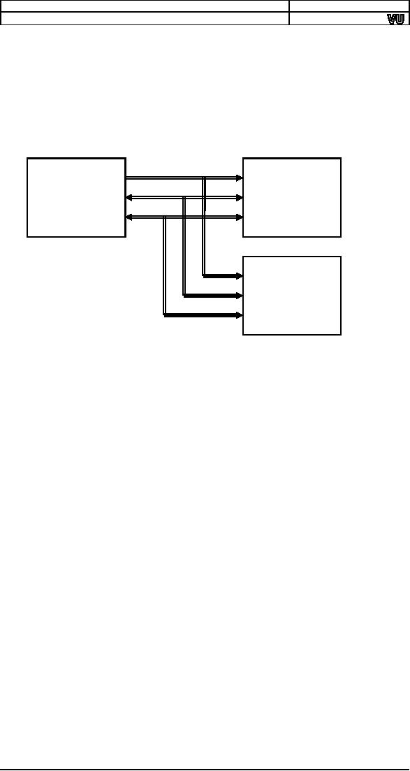
PROCESSOR
MEMORY
PERIPHERALS
We take
an example to explain the
collaboration of the processor
and
memory
using the address, control,
and data buses. Consider
that you want
your
uneducated servant to bring a
book from the shelf.
You order him to
bring
the fifth book from
top of the shelf. All the
data movement
operations
are
hidden in this one sentence.
Such a simple everyday
phenomenon seen
from
this perspective explains
the seemingly complex
working of the three
buses.
We told the servant to
"bring a book" and the
one which is "fifth
from
top,"
precise location even for
the servant who is much more
intelligent then
our dumb
memory. The dumb servant
follows the steps one by
one and the
book is
in your hand as a result. If
however you just asked him
for a book or
you
named the book, your
uneducated servant will stand
there gazing at you
and
the book will never come in
your hand.
Even in
this simplest of all
examples, mathematics is there,
"fifth from
top."
Without a number the servant
would not be able to locate
the book. He
is
unable to understand your
will. Then you tell him to
put it with the
seventh
book on the right shelf.
Precision is involved and
only numbers are
precise
in this world. One will
always be one and two will
always be two. So
we tell
in the form of a number on
the address bus which cell is
needed out
of say
the 2000 cells in the
whole memory.
A
binary number is generated on
the address bus, fifth,
seventh, eighth,
tenth;
the cell which is needed. So
the cell number is placed on
the address
bus. A
memory cell is an n-bit
location to store data,
normally 8-bit also
called
a byte. The number of bits
in a cell is called the cell
width. The
two
dimensions,
cell width and number of
cells, define the memory
completely
just
like the width and depth of
a well defines it completely.
200 feet deep by
15 feet
wide and the well is
completely described. Similarly
for memory we
define
two dimensions. The first
dimension defines how many parallel
bits
are
there in a single memory
cell. The memory is called
8-bit or 16-bit for
this
reason and this is also
the word size of the
memory. This need
not
match
the size of a processor word
which has other parameters to
define it.
In
general the memory cell
cannot be wider than the
width of the data
bus.
Best
and simplest operation
requires the same size of
data bus and memory
cell
width.
2

Computer
Architecture & Assembly Language
Programming
Course
Code: CS401
CS401@vu.edu.pk
As we
previously discussed that
the control bus carries the
intent of the
processor
that it wants to read or to
write. Memory changes its
behavior in
response
to this signal from the
processor. It defines the
direction of data
flow.
If processor wants to read but
memory wants to write, there
will be no
communication
or useful flow of information.
Both must be synchronized,
like a
speaker speaks and the
listener listens. If both
speak simultaneously
or both
listen there will be no communication.
This precise
synchronization
between
the processor and the
memory is the responsibility of
the control
bus.
Control
bus is only the mechanism.
The responsibility of sending
the
appropriate
signals on the control bus to
the memory is of the
processor.
Since
the memory never wants to
listen or to speak of itself.
Then why is the
control
bus bidirectional. Again we take
the same example of the
servant and
the
book further to elaborate
this situation. Consider
that the servant
went
to
fetch the book just to
find that the drawing
room door is locked. Now
the
servant
can wait there indefinitely
keeping us in surprise or come
back and
inform
us about the situation so
that we can act accordingly.
The servant
even
though he was obedient was unable to
fulfill our orders so in all
his
obedience,
he came back to inform us
about the problem.
Synchronization is
still
important, as a result of our orders
either we got the desired
cell or we
came to
know that the memory is
locked for the moment.
Such information
cannot
be transferred via the
address or the data bus.
For such situations
when
peripherals want to talk to the
processor when the processor
wasn't
expecting
them to speak, special lines in
the control bus are used.
The
information
in such signals is usually to
indicate the incapability of
the
peripheral
to do something for the
moment. For these reasons
the control
bus is a
bidirectional bus and can
carry information from
processor to
memory
as well as from memory to
processor.
1.2.
REGISTERS
The
basic purpose of a computer is to
perform operations, and
operations
need
operands. Operands are the
data on which we want to perform a
certain
operation.
Consider the addition
operation; it involves adding two
numbers
to get
their sum. We can have
precisely one address on the
address bus and
consequently
precisely one element on the
data bus. At the very
same instant
the
second operand cannot be
brought inside the
processor. As soon as
the
second
is selected, the first
operand is no longer there.
For this reason
there
are
temporary storage places
inside the processor called
registers. Now
one
operand
can be read in a register
and added into the
other which is read
directly
from the memory. Both
are made accessible at one
instance of time,
one
from inside the processor
and one from outside on
the data bus.
The
result
can be written to at a distinct
location as the operation
has completed
and we
can access a different
memory cell. Sometimes we
hold both
operands
in registers for the sake of
efficiency as what we can do inside
the
processor
is undoubtedly faster than if we
have to go outside and bring
the
second
operand.
Registers
are like a scratch pad ram
inside the processor and
their
operation
is very much like normal
memory cells. They have
precise locations
and
remember what is placed inside
them. They are used when we
need
more
than one data element
inside the processor at one
time. The concept of
registers
will be further elaborated as we progress
into writing our
first
program.
Memory
is a limited resource but the
number of memory cells is
large.
Registers
are relatively very small in
number, and are therefore a
very scarce
and
precious resource. Registers
are more than one in
number, so we have to
precisely
identify or name them. Some
manufacturers number their
registers
like
r0, r1, r2, others
name them like A, B, C, D etc.
Naming is useful
since
the
registers are few in number.
This is called the
nomenclature of the
3
Computer
Architecture & Assembly Language
Programming
Course
Code: CS401
CS401@vu.edu.pk
particular
architecture. Still other
manufacturers name their
registers
according
to their function like X
stands for an index
register. This also
informs
us that there are special
functions of registers as well,
some of which
are
closely associated to the
particular architecture. For
example index
registers
do not hold data instead
they are used to hold
the address of data.
There
are other functions as well
and the whole spectrum of
register
functionalities
is quite large. However most
of the details will become
clear as
the
registers of the Intel
architecture are discussed in
detail.
Accumulator
There
is a central register in every
processor called the
accumulator.
Traditionally
all mathematical and logical
operations are performed on
the
accumulator.
The word size of a processor
is defined by the width of
its
accumulator.
A 32bit processor has an
accumulator of 32 bits.
Pointer, Index, or
Base Register
The
name varies from
manufacturer to manufacturer, but the
basic
distinguishing
property is that it does not
hold data but holds the
address of
data.
The rationale can be
understood by examining a "for"
loop in a higher
level
language, zeroing elements in an
array of ten elements
located in
consecutive
memory cells. The location
to be zeroed changes every
iteration.
That is
the address where the
operation is performed is changing.
Index
register
is used in such a situation to
hold the address of the
current array
location.
Now the value in the index
register cannot be treated as
data, but it
is the
address of data. In general
whenever we need access to a
memory
location
whose address is not known until
runtime we need an
index
register.
Without this register we
would have needed to
explicitly code each
iteration
separately.
In
newer architectures the
distinction between accumulator
and index
registers
has become vague. They
have general registers which
are more
versatile
and can do both functions.
They do have some
specialized behaviors
but
basic operations can be done
on all general
registers.
Flags Register or
Program Status
Word
This is
a special register in every
architecture called the
flags register or
the
program status word. Like
the accumulator it is an 8, 16, or 32
bits
register
but unlike the accumulator it is
meaningless as a unit, rather
the
individual
bits carry different
meanings. The bits of the
accumulator work in
parallel
as a unit and each bit mean
the same thing. The
bits of the flags
register
work independently and individually,
and combined its value
is
meaningless.
An
example of a bit commonly present in
the flags register is the
carry flag.
The
carry can be contained in a
single bit as in binary arithmetic
the carry
can
only be zero or one. If a
16bit number is added to a
16bit accumulator,
and
the result is of 17 bits the
17th bit is placed in the
carry bit of the
flags
register.
Without this 17th bit the
answer is incorrect. More
examples of flags
will be
discussed when dealing with the
Intel specific register
set.
Program Counter or
Instruction Pointer
Everything
must translate into a binary
number for our dumb processor
to
understand
it, be it an operand or an operation
itself. Therefore the
instructions
themselves must be translated into
numbers. For example
to
add
numbers we understand the
word "add." We translate
this word into a
number
to make the processor
understand it. This number
is the actual
instruction
for the computer. All the
objects, inheritance and
encapsulation
constructs
in higher level languages
translate down to just a number
in
assembly
language in the end.
Addition, multiplication, shifting;
all big
4

Computer
Architecture & Assembly Language
Programming
Course
Code: CS401
CS401@vu.edu.pk
programs
are made using these
simple building blocks. A
number is at the
bottom
line since this is the
only thing a computer can
understand.
A
program is defined to be "an
ordered set of instructions."
Order in this
definition
is a key part. Instructions run
one after another, first,
second,
third
and so on. Instructions have
a positional relationship. The
whole logic
depends
on this positioning. If the
computer executes the fifth
instructions
after
the first and not
the second, all our logic is
gone. The processor
should
ensure
this ordering of instructions. A
special register exists in
every
processor
called the program counter
or the instruction pointer
that ensures
this
ordering. "The program
counter holds the address of
the next instruction
to be
executed." A number is placed in
the memory cell pointed to
by this
register
and that number tells
the processor which instruction to
execute; for
example
0xEA, 255, or 152. For
the processor 152 might be
the add
instruction.
Just this one number tells
it that it has to add, where
its
operands
are, and where to store
the result. This number is
called the
opcode. The
instruction pointer moves
from one opcode to the
next. This is
how our
program executes and
progresses. One instruction is
picked, its
operands
are read and the
instruction is executed, then
the next instruction
is
picked from the new address
in instruction pointer and so
on.
Remembering
152 for the add
operation or 153 for the
subtract operation
is
difficult. To make a simple way to
remember difficult things we
associate a
symbol
to every number. As when we write
"add" everyone understands
what
we mean
by it. Then we need a small
program to convert this
"add" of ours to
152
for the processor. Just a
simple search and replace
operation to
translate
all such symbols to their
corresponding opcodes. We have
mapped
the
numeric world of the
processor to our symbolic world.
"Add" conveys a
meaning
to us but the number 152
does not. We can say
that add is closer to
the
programmer's thinking. This is
the basic motive of adding
more and more
translation
layers up to higher level
languages like C++ and
Java and Visual
Basic.
These symbols are called
instruction
mnemonics.
Therefore the
mnemonic
"add a to b" conveys more
information to the reader.
The dumb
translator
that will convert these
mnemonics back to the
original opcodes is
a key
program to be used throughout
this course and is called
the assembler.
1.3.
INSTRUCTION GROUPS
Usual
opcodes in every processor
exist for moving data,
arithmetic and
logical
manipulations etc. However
their mnemonics vary
depending on the
will of
the manufacturer. Some
manufacturers name the
mnemonics for data
movement
instructions as "move," some
call it "load" and "store"
and still
other
names are present. But the
basic set of instructions is
similar in every
processor.
A grouping of these instructions
makes learning a new
processor
quick
and easy. Just the group an
instruction belongs tells a
lot about the
instruction.
Data
Movement Instructions
These
instructions are used to
move data from one
place to another.
These
places
can be registers, memory, or
even inside peripheral
devices. Some
examples
are:
mov
ax, bx
lad
1234
Arithmetic
and Logic
Instructions
Arithmetic
instructions like addition,
subtraction, multiplication,
division
and
Logical instructions like
logical and, logical or,
logical xor, or
complement
are part of this group.
Some examples are:
and
ax,
1234
add
bx,
0534
add
bx, [1200]
5

Computer
Architecture & Assembly Language
Programming
Course
Code: CS401
CS401@vu.edu.pk
The
bracketed form is a complex
variation meaning to add the
data placed
at
address 1200. Addressing
data in memory is a detailed
topic and is
discussed
in the next chapter.
Program
Control Instructions
The
instruction pointer points to
the next instruction and
instructions run
one
after the other with the
help of this register. We
can say that
the
instructions
are tied with one another.
In some situations we don't want
to
follow
this implied path and want
to order the processor to
break its flow if
some
condition becomes true
instead of the spatially
placed next
instruction.
In
certain other cases we want
the processor to first
execute a separate
block
of code
and then come back to
resume processing where it
left.
These
are instructions that
control the program
execution and flow by
playing
with the instruction pointer
and altering its normal
behavior to point
to the
next instruction. Some
examples are:
cmp
ax, 0
jne
1234
We are
changing the program flow to
the instruction at 1234
address if the
condition
that we checked becomes
true.
Special
Instructions
Another
group called special
instructions works like the
special service
commandos.
They allow changing specific
processor behaviors and are
used
to play
with it. They are used
rarely but are certainly
used in any
meaningful
program.
Some examples are:
cli
sti
Where
cli clears the interrupt
flag and sti sets
it. Without delving deep
into
it,
consider that the cli
instruction instructs the
processor to close its
ears
from
the outside world and
never listen to what is happening
outside,
possibly
to do some very important
task at hand, while sti
restores normal
behavior.
Since these instructions
change the processor
behavior they are
placed
in the special instructions
group.
1.4.
INTEL IAPX88
ARCHITECTURE
Now we
select a specific architecture to
discuss these abstract ideas
in
concrete
form. We will be using IBM PC based on
Intel architecture
because
of its
wide availability, because of
free assemblers and
debuggers available
for
it, and because of its
wide use in a variety of
domains. However the
concepts
discussed will be applicable on any
other architecture as well;
just
the
mnemonics of the particular
language will be different.
Technically
iAPX88 stands for "Intel
Advanced Processor Extensions
88." It
was a
very successful processor
also called 8088 and was
used in the very
first
IBM PC machines. Our discussion will
revolve around 8088 in the
first
half of
the course while in the
second half we will use
iAPX386 which is very
advanced
and powerful processor. 8088
is a 16bit processor with
its
accumulator
and all registers of 16
bits. 386 on the other
hand, is a 32bit
processor.
However it is downward compatible with
iAPX88 meaning that
all
code
written for 8088 is valid on
the 386. The architecture of
a processor
means
the organization and
functionalities of the registers it
contains and
the
instructions that are valid
on the processor. We will discuss
the register
architecture
of 8088 in detail below
while its instructions are
discussed in
the
rest of the book at
appropriate places.
1.5.
HISTORY
Intel
did release some 4bit
processors in the beginning but
the first
meaningful
processor was 8080, an 8bit
processor. The processor
became
6
Computer
Architecture & Assembly Language
Programming
Course
Code: CS401
CS401@vu.edu.pk
popular
due to its simplistic design
and versatile architecture.
Based on the
experience
gained from 8080, an
advanced version was released as
8085.
The
processor became widely
popular in the engineering
community again
due to
its simple and logical
nature.
Intel
introduced the first 16bit
processor named 8088 at a
time when the
concept
of personal computer was
evolving. With a maximum memory of
64K
on the
8085, the 8088 allowed a
whole mega byte. IBM
embedded this
processor
in their personal computer.
The first machines ran at
4.43 MHz; a
blazing
speed at that time. This was
the right thing at the
right moment. No
one
expected this to become the
biggest success of computing
history. IBM
PC XT
became so popular and
successful due to its open
architecture and
easily
available information.
The
success was unexpected for
the developers themselves. As when
Intel
introduced
the processor it contained a
timer tick count which was
valid for
five
years only. They never
anticipated the architecture to
stay around for
more
than five years but the
history took a turn and the
architecture is there
at
every desk even after 25
years and the tick is to be
specially handled
every
now and
then.
1.6.
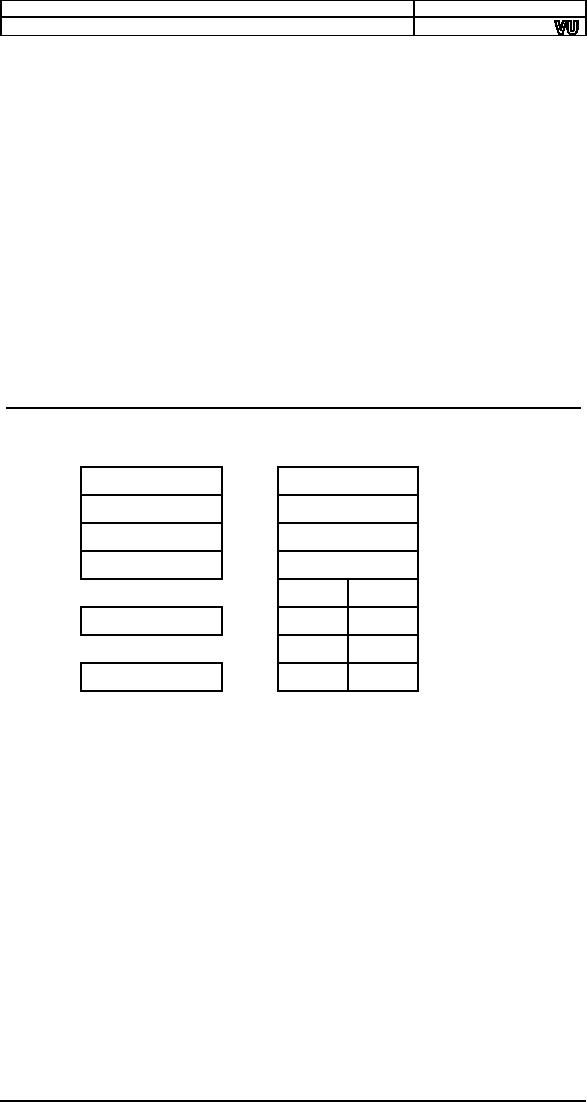
REGISTER ARCHITECTURE
The
iAPX88 architecture consists of 14
registers.
CS
SP
DS
BP
SS
SI
ES
DI
(AX)
AH
AL
(BX)
IP
BH
BL
(CX)
CH
CL
(DX)
DH
DL
FLAGS
General Registers
(AX, BX, CX, and
DX)
The
registers AX, BX, CX, and DX behave as
general purpose registers
in
Intel
architecture and do some
specific functions in addition to
it. X in their
names
stand for extended meaning
16bit registers. For example
AX means
we are
referring to the extended
16bit "A" register. Its
upper and lower
byte
are
separately accessible as AH (A high
byte) and AL (A low byte). All
general
purpose
registers can be accessed as
one 16bit register or as two
8bit
registers.
The two registers AH and AL
are part of the big
whole AX. Any
change
in AH or AL is reflected in AX as well. AX is a
composite or extended
register
formed by gluing together
the two parts AH and
AL.
The A
of AX stands for Accumulator.
Even though all general
purpose
registers
can act as accumulator in
most instructions there are
some specific
variations
which can only work on AX which is why it is
named the
accumulator.
The B of BX stands for Base
because of its role in
memory
addressing
as discussed in the next
chapter. The C of CX stands
for Counter
as
there are certain
instructions that work with an automatic
count in the
CX
register. The D of DX stands
for Destination as it acts as
the destination
in I/O
operations. The A, B, C, and D
are in letter sequence as
well as depict
some
special functionality of the
register.
7
Computer
Architecture & Assembly Language
Programming
Course
Code: CS401
CS401@vu.edu.pk
Index Registers
(SI and DI)
SI and
DI stand for source index
and destination index
respectively. These
are
the index registers of the
Intel architecture which hold
address of data
and
used in memory access. Being
an open and flexible
architecture, Intel
allows
many mathematical and logical
operations on these registers as
well
like
the general registers. The
source and destination are
named because of
their
implied functionality as the
source or the destination in a
special class
of
instructions called the
string instructions. However
their use is not at
all
restricted
to string instructions. SI and DI
are 16bit and cannot be
used as
8bit
register pairs like AX, BX, CX,
and DX.
Instruction
Pointer (IP)
This is
the special register
containing the address of
the next instruction
to
be
executed. No mathematics or memory
access can be done through
this
register.
It is out of our direct control and is
automatically used. Playing
with
it is
dangerous and needs special
care. Program control
instructions change
the IP
register.
Stack
Pointer (SP)
It is a
memory pointer and is used
indirectly by a set of instructions.
This
register
will be explored in the discussion of
the system stack.
Base
Pointer (BP)
It is
also a memory pointer
containing the address in a
special area of
memory
called the stack and will be
explored alongside SP in the
discussion
of the
stack.
Flags
Register
The
flags register as previously
discussed is not meaningful as a
unit
rather
it is bit wise significant and
accordingly each bit is named
separately.
The
bits not named are
unused. The Intel FLAGS
register has its
bits
organized
as follows:
15
14
13
12
11
10
9
8
7
6
5
4
3
2
1
0
O
D
I
T
S
Z
A
P
C
The
individual flags are
explained in the following
table.
C
Carry
When
two 16bit numbers are added
the answer can be
17 bits
long or when two 8bit numbers
are added the
answer
can be 9 bits long. This
extra bit that won't
fit
in the
target register is placed in
the carry flag where
it
can be
used and tested.
P
Parity
Parity
is the number of "one" bits
in a binary number.
Parity
is either odd or even. This
information is
normally
used in communications to verify
the integrity
of data
sent from the sender to
the receiver.
A
Auxiliary
A
number in base 16 is called a
hex number and can
be
Carry
represented
by 4 bits. The collection of 4
bits is called a
nibble.
During addition or subtraction if a
carry goes
from
one nibble to the next
this flag is set. Carry
flag is
for
the carry from the
whole addition while
auxiliary
carry
is the carry from the
first nibble to the
second.
Z
Zero
Flag
The
Zero flag is set if the
last mathematical or
logical
instruction
has produced a zero in its
destination.
8
Computer
Architecture & Assembly Language
Programming
Course
Code: CS401
CS401@vu.edu.pk
S
Sign
Flag
A
signed number is represented in
its two's complement
form in
the computer. The most
significant bit (MSB) of
a
negative number in this
representation is 1 and for
a
positive
number it is zero. The sign
bit of the last
mathematical
or logical operation's destination
is
copied
into the sign
flag.
T
Trap
Flag
The
trap flag has a special
role in debugging which will
be
discussed later.
I
Interrupt
Flag
It
tells whether the processor
can be interrupted
from
outside
or not. Sometimes the
programmer doesn't
want a
particular task to be interrupted so
the
Interrupt
flag can be zeroed for
this time. The
programmer
rather than the processor
sets this flag
since
the programmer knows when
interruption is okay
and
when it is not. Interruption can be
disabled or
enabled
by making this bit zero or
one, respectively,
using
special instructions.
D
Direction
Flag
Specifically
related to string instructions,
this flag tells
whether
the current operation has to
be done from
bottom
to top of the block (D=0) or
from top to bottom
of the
block (D=1).
O
Overflow
Flag
The
overflow flag is set during
signed arithmetic,
e.g.
addition
or subtraction, when the
sign of the
destination
changes unexpectedly. The
actual process
sets
the overflow flag whenever
the carry into the
MSB
is
different from the carry out
of the MSB
Segment Registers
(CS, DS, SS, and
ES)
The
code segment register, data
segment register, stack
segment register,
and
the extra segment register
are special registers
related to the Intel
segmented
memory model and will be
discussed later.
1.7.
OUR FIRST PROGRAM
The
first program that we will
write will only add three
numbers. This very
simple
program will clarify most of
the basic concepts of
assembly language.
We will
start with writing our algorithm in
English and then moving on
to
convert
it into assembly
language.
English
Language Version
"Program
is an ordered set of instructions
for the processor." Our
first
program
will be instructions manipulating AX and
BX in plain English.
move 5 to
ax
move 10 to
bx
add bx to
ax
move 15 to
bx
add bx to
ax
Even in
this simple reflection of
thoughts in English, there
are some key
things
to observe. One is the
concept of destination as every
instruction has
a "to
destination" part and there
is a source before it as well.
For example the
second
line has a constant 10 as
its source and the
register BX as its
destination.
The key point in giving
the first program in English
is to convey
that
the concepts of assembly
language are simple but
fine. Try to
understand
them considering that all
above is everyday English
that you
know
very well and every
concept will eventually be applicable to
assembly
language.
9
Computer
Architecture & Assembly Language
Programming
Course
Code: CS401
CS401@vu.edu.pk
Assembly
Language Version
Intel
could have made their
assembly language exactly
identical to our
program
in plain English but they
have abbreviated a lot of
symbols to avoid
unnecessarily
lengthy program when the
meaning could be conveyed
with
less
effort. For example Intel
has named their move
instruction "mov"
instead
of
"move." Similarly the Intel
order of placing source and
destination is
opposite
to what we have used in our English
program, just a change
of
interpretation.
So the Intel way of writing
things is:
operation destination,
source
operation
destination
operation
source
operation
The
later three variations are
for instructions that have
one or both of their
operands
implied or they work on a single or no
operand. An implied
operand
means
that it is always in a particular
register say the
accumulator, and it
need
not be mentioned in the
instruction. Now we attempt to write
our
program
in actual assembly language of
the iapx88.
Example
1.1
001
; a program to
add
three numbers
using registers
002
[org
0x0100]
003
mov
ax,
5
;
load first number
in ax
004
mov
bx,
10
;
load second
number in bx
005
add
ax,
bx
;
accumulate
sum in ax
006
mov
bx,
15
;
load third number
in bx
007
add
ax,
bx
;
accumulate
sum in ax
008
009
mov
ax,
0x4c00
; terminate
program
010
int
0x21
To
start a comment a semicolon is
used and the assembler
ignores
001
everything
else on the same line.
Comments must be extensively
used in
assembly language programs to
make them readable.
Leave
the org directive for now as
it will be discussed later.
002
The
constant 5 is loaded in one
register AX.
003
The
constant 10 is loaded in another
register BX.
004
Register
BX is added to register AX and
the result is stored
in
005
register
AX. Register AX should contain 15 by
now.
The
constant 15 is loaded in the
register BX.
006
Register
BX is again added to register AX now
producing 15+15=30
007
in the
AX register. So the program
has computed
5+10+15=30.
Vertical
spacing must also be used
extensively in assembly
language
008
programs
to separate logical blocks of
code.
The
ending lines are related
more to the operating system
than to
009-010
assembly
language programming. It is a way to
inform DOS that our
program
has terminated so it can
display its command
prompt
again.
The computer may reboot or
behave improperly if
this
termination
is not present.
Assembler,
Linker, and Debugger
We need
an assembler to assemble this
program and convert this
into
executable
binary code. The assembler
that we will use during this
course is
"Netwide
Assembler" or NASM. It is a free
and open source assembler.
And
the
tool that will be most used
will be the debugger. We will use a
free
debugger
called "A fullscreen debugger" or
AFD. These are the
whole set of
10
Computer
Architecture & Assembly Language
Programming
Course
Code: CS401
CS401@vu.edu.pk
weapons
an assembly language programmer
needs for any task
whatsoever
at
hand.
To
assemble we will give the
following command to the
processor assuming
that
our input file is named
EX01.ASM.
nasm
ex01.asm o ex01.com l
ex01.lst
This
will produce two files EX01.COM
that is our executable file
and
EX01.LST
that is a special listing
file that we will explore
now. The listing
file
produced
for our example above is
shown below with comments
removed for
neatness.
1
2
[org
0x0100]
3
00000000
B80500
mov
ax,
5
4
00000003
BB0A00
mov
bx,
10
5
00000006
01D8
add
ax,
bx
6
00000008
BB0F00
mov
bx,
15
7
0000000B
01D8
add
ax,
bx
8
9
0000000D
B8004C
mov
ax,
0x4c00
10
00000010
CD21
int
0x21
The
first column in the above
listing is offset of the
listed instruction in
the
output
file. Next column is the
opcode into which our instruction
was
translated.
In this case this opcode is
B8. Whenever we move a constant
into
AX
register the opcode B8 will be
used. After it 0500 is
appended which is
the
immediate operand to this
instruction. An immediate operand is
an
operand
which is placed directly inside
the instruction. Now as the
AX
register
is a word sized register,
and one hexadecimal digit
takes 4 bits so 4
hexadecimal
digits make one word or two
bytes. Which of the two
bytes
should
be placed first in the
instruction, the least
significant or the
most
significant?
Similarly for 32bit numbers
either the order can be
most
significant,
less significant, lesser
significant, and least
significant called
the
big-endian
order used by Motorola and
some other companies or it
can be
least
significant, more significant,
more significant, and most
significant
called
the little-endian order and
is used by Intel. The
big-endian have the
argument
that it is more natural to
read and comprehend while
the little-
endian
have the argument that
this scheme places the
less significant
value
at a
lesser address and more
significant value at a higher
address.
Because
of this the constant 5 in our
instruction was converted into
0500
with
the least significant byte
of 05 first and the most
significant byte of 00
afterwards.
When read as a word it is
0005 but when written in memory
it
will
become 0500. As the first
instruction is three bytes
long, the listing
file
shows
that the offset of the
next instruction in the file
is 3. The opcode BB is
for
moving a constant into the
BX register, and the operand
0A00 is the
number
10 in little-endian byte order.
Similarly the offsets and
opcodes of
the
remaining instructions are
shown in order. The last
instruction is placed
at
offset 0x10 or 16 in decimal. The
size of the last instruction
is two bytes,
so the
size of the complete COM
file becomes 18 bytes. This
can be verified
from
the directory listing, using
the DIR command, that the
COM file
produced
is exactly 18 bytes
long.
Now the
program is ready to be run inside
the debugger. The
debugger
shows
the values of registers,
flags, stack, our code, and
one or two areas of
the
system memory as data.
Debugger allows us to step our
program one
instruction
at a time and observe its
effect on the registers and
program
data.
The details of using the
AFD debugger can be seen
from the AFD
manual.
After
loading the program in the
debugger observe that the
first instruction
is now at
0100 instead of absolute
zero. This is the effect of
the org directive
at the
start of our program. The
first instruction of a COM file must be
at
11

Computer
Architecture & Assembly Language
Programming
Course
Code: CS401
CS401@vu.edu.pk
offset
0100 (decimal 255) as a
requirement. Also observe
that the debugger is
showing
your program even though it
was provided only the COM
file and
neither
of the listing file or the
program source. This is
because the
translation
from mnemonic to opcode is
reversible and the debugger
mapped
back
from the opcode to the
instruction mnemonic. This will
become
apparent
for instructions that have
two mnemonics as the debugger
might
not
show the one that was
written in the source
file.
As a
result of program execution
either registers or memory will
change.
Since
our program yet doesn't
touch memory the only
changes will be in the
registers.
Keenly observe the registers
AX, BX, and IP change after
every
instruction.
IP will change after every
instruction to point to the
next
instruction
while AX will accumulate the
result of our addition.
1.8.
SEGMENTED MEMORY
MODEL
Rationale
In
earlier processors like 8080
and 8085 the linear
memory model was
used to
access memory. In linear
memory model the whole
memory appears
like a
single array of data. 8080
and 8085 could access a
total memory of
64K
using the 16 lines of their
address bus. When designing
iAPX88 the Intel
designers
wanted to remain compatible with
8080 and 8085 however
64K
was
too small to continue with,
for their new processor. To
get the best of
both
worlds they introduced the
segmented memory model in
8088.
There
is also a logical argument in
favor of a segmented memory
model in
additional
to the issue of compatibility
discussed above. We have two
logical
parts
of our program, the code and
the data, and actually
there is a third
part
called the program stack as
well, but higher level
languages make this
invisible
to us. These three logical
parts of a program should
appear as three
distinct
units in memory, but making
this division is not
possible in the
linear
memory model. The segmented
memory model does allow
this
distinction.
Mechanism
The
segmented memory model
allows multiple functional
windows into the
main
memory, a code window, a
data window etc. The
processor sees code
from
the code window and data
from the data window.
The size of one
window is
restricted to 64K. 8085
software fits in just one
such window. It
sees
code, data, and stack
from this one window, so
downward compatibility
is
attained.
However
the maximum memory iAPX88
can access is 1MB which can
be
accessed
with 20 bits. Compare this with
the 64K of 8085 that were
accessed
using
16 bits. The idea is that
the 64K window just discussed can be
moved
anywhere
in the whole 1MB. The four
segment registers discussed in
the
Intel
register architecture are
used for this purpose.
Therefore four
windows
can
exist at one time. For
example one window that is
pointed to by the CS
register
contains the currently
executing code.
To
understand the concept,
consider the windows of a
building. We say
that a
particular window is 3 feet
above the floor and
another one is 20
feet
above
the floor. The reference
point, the floor is the
base of the segment
called
the datum point in a graph
and all measurement is done
from that
datum
point considering it to be zero. So CS
holds the zero or the
base of
code.
DS holds the zero of data.
Or we can say CS tells how
high code from
the
floor is, and DS tells how
high data from the
floor is, while SS tells
how
high
the stack is. One
extra segment ES can be used
if we need to access two
distant
areas of memory at the same
time that both cannot be
seen through
the
same window. ES also has
special role in string
instructions. ES is used
as an
extra data segment and
cannot be used as an extra
code or stack
segment.
12
Computer
Architecture & Assembly Language
Programming
Course
Code: CS401
CS401@vu.edu.pk
Revisiting
the concept again, like
the datum point of a graph,
the segment
registers
tell the start of our window
which can be opened anywhere in
the
megabyte
of memory available. The window is of a
fixed size of 64KB.
Base
and
offset are the two key
variables in a segmented address.
Segment tells
the
base while offset is added
into it. The registers
IP, SP, BP, SI, DI,
and BX
all
can contain a 16bit offset
in them and access memory
relative to a
segment
base.
The IP
register cannot work alone. It
needs the CS register to
open a 64K
window in
the 1MB memory and then IP
works to select code from
this
window as
offsets. IP works only
inside this window and
cannot go outside of
this
64K in any case. If the window is
moved i.e. the CS register
is changed,
IP will
change its behavior
accordingly and start
selecting from the
new
window.
The IP register always works
relatively, relative to the
segment base
stored
in the CS register. IP is a 16bit
register capable of accessing
only 64K
memory
so how the whole megabyte
can contain code anywhere.
Again the
same
concept is there, it can
access 64K at one instance of
time. As the base
is
changed using the CS
register, IP can be made to
point anywhere is the
whole
megabyte. The process is
illustrated with the following
diagram.
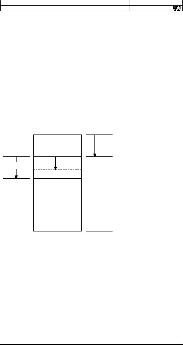
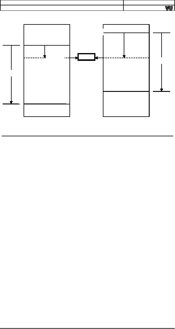
Physical
Address
00000
Segment
Base
xxxx0
Offset
Paragraph
64K
Boundary
FFFFF
Physical
Address Calculation
Now for
the whole megabyte we need
20 bits while CS and IP are
both
16bit
registers. We need a mechanism to
make a 20bit number out of
the two
16bit
numbers. Consider that the
segment value is stored as a 20 bit
number
with
the lower four bits
zero and the offset
value is stored as another 20
bit
number
with the upper four bits
zeroed. The two are added to
produce a
20bit
absolute address. A carry if
generated is dropped without
being stored
anywhere
and the phenomenon is called
address wraparound. The
process is
explained
with the help of the
following diagram.
13
Computer
Architecture & Assembly Language
Programming
Course
Code: CS401
CS401@vu.edu.pk
15----------------------------0
Segment
Address
16bit Segment
Register
0000
15----------------------------0
Offset
Address
0000
16bit Logical
Address
19-----------------------------------0
20bit Physical
Address
Therefore
memory is determined by a segment-offset
pair and not alone
by
any
one register which will be an ambiguous
reference. Every offset
register
is
assigned a default segment
register to resolve such
ambiguity. For
example
the
program we wrote when loaded
into memory had a value of
0100 in IP
register
and some value say 1DDD in
the CS register. Making both
20 bit
numbers,
the segment base is 1DDD0
and the offset is 00100
and adding
them we
get the physical memory
address of 1DED0 where the
opcode
B80500
is placed.
Paragraph
Boundaries
As the
segment value is a 16bit
number and four zero
bits are appended to
the
right to make it a 20bit
number, segments can only be
defined a 16byte
boundaries
called paragraph boundaries.
The first possible segment
value is
0000
meaning a physical base of
00000 and the next
possible value of
0001
means a
segment base of 00010 or 16 in
decimal. Therefore segments
can
only be
defined at 16 byte
boundaries.
Overlapping
Segments
We can
also observe that in the
case of our program CS, DS,
SS, and ES
all
had the same value in
them. This is called
overlapping segments so
that
we can
see the same memory
from any window. This is
the structure of a
COM
file.
Using
partially overlapping segments we
can produce a number
of
segment,
offset pairs that all
access the same memory.
For example
1DDD:0100
and IDED:0000 both point to
the same physical memory. To
test
this we
can open a data window at
1DED:0000 in the debugger
and change
the
first three bytes to "90"
which is the opcode for NOP
(no operation). The
change
is immediately visible in the
code window which is pointed to by
CS
containing
1DDD. Similarly IDCD:0200
also points to the same
memory
location.
Consider this like a portion
of wall that three different
people on
three
different floors are seeing
through their own windows.
One of them
painted
the wall red; it will be changed
for all of them though
their
perspective
is different. It is the same
phenomenon occurring
here.
The
segment, offset pair is
called a logical address,
while the 20bit
address
is a
physical address which is the
real thing. Logical
addressing is a
mechanism
to access the physical
memory. As we have seen
three different
logical
addresses accessed the same
physical address.
14
Computer
Architecture & Assembly Language
Programming
Course
Code: CS401
CS401@vu.edu.pk
00000
1DCD0
Offset
1DDD0
0200
Offset
0100
1DED0
64K
64K
FFFFF
EXERCISES
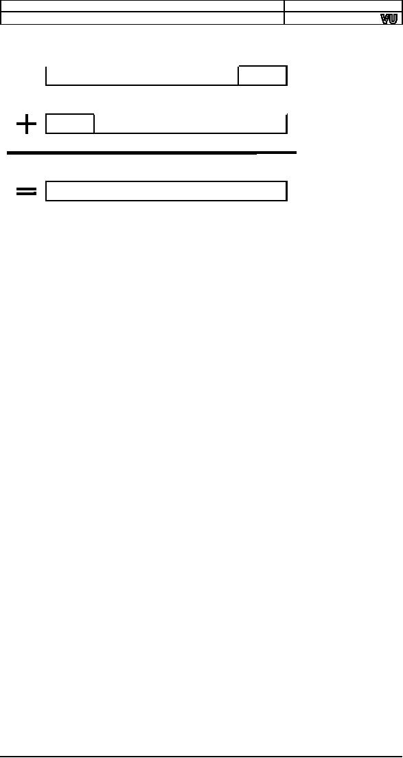
1.
How the
processor uses the address
bus, the data bus,
and the
control
bus to communicate with the system
memory?
2.
Which
of the following are
unidirectional and which are
bidirectional?
a.
Address Bus
b. Data
Bus
c.
Control Bus
3.
What
are registers and what are
the specific features of
the
accumulator,
index registers, program
counter, and program
status
word?
4.
What is
the size of the accumulator
of a 64bit processor?
5.
What is
the difference between an
instruction mnemonic and
its
opcode?
6.
How are
instructions classified into
groups?
7.
A
combination of 8bits is called a
byte. What is the name
for 4bits and
for
16bits?
8.
What is
the maximum memory 8088 can
access?
9.
List
down the 14 registers of the
8088 architecture and
briefly
describe
their uses.
10.
What
flags are defined in the
8088 FLAGS register?
Describe the
function
of the zero flag, the
carry flag, the sign
flag, and the
overflow
flag.
11.
Give
the value of the zero
flag, the carry flag,
the sign flag, and
the
overflow
flag after each of the
following instructions if AX is
initialized
with
0x1254 and BX is initialized with
0x0FFF.
a. add
ax, 0xEDAB
b. add
ax, bx
c. add
bx, 0xF001
12.
What is
the difference between
little endian and big
endian formats?
Which
format is used by the Intel
8088 microprocessor?
13.
For
each of the following words
identify the byte that is
stored at lower
memory
address and the byte
that is stored at higher
memory address
in a
little endian
computer.
a.
1234
b.
ABFC
c.
B100
d.
B800
15

Computer
Architecture & Assembly Language
Programming
Course
Code: CS401
CS401@vu.edu.pk
14.
What are the contents of
memory locations 200, 201,
202, and 203 if
the
word 1234 is stored at
offset 200 and the
word 5678 is stored
at
offset
202?
15.
What is the offset at which
the first executable
instruction of a COM
file
must be placed?
16. Why
was segmentation originally introduced in
8088 architecture?
17. Why
a segment start cannot start
from the physical address
55555.
18.
Calculate the physical
memory address generated by
the following
segment
offset pairs.
a.
1DDD:0436
b.
1234:7920
c.
74F0:2123
d.
0000:6727
e.
FFFF:4336
f.
1080:0100
g.
AB01:FFFF
19.
What are the first
and the last physical
memory addresses
accessible
using
the following segment
values?
a.
1000
b.
0FFF
c.
1002
d.
0001
e.
E000
20.
Write instructions that
perform the following
operations.
a. Copy
BL into CL
b. Copy
DX into AX
c.
Store 0x12 into AL
d.
Store 0x1234 into AX
e.
Store 0xFFFF into AX
21.
Write a program in assembly
language that calculates the
square of
six by
adding six to the accumulator six
times.
16
Table of Contents:
- Introduction to Assembly Language Programming
- Addressing Modes: Data Declaration, Direct, Register Indirect , Offset Addressing
- Branching: Comparison and Conditions, Conditional ,Unconditional Jump
- Manipulations: Multiplication Algorithm, Shifting and Rotations, Bitwise Logical Operations
- Subroutines: Program Flow, Stack, Saving and Restoring Registers
- Display Memory: ASCII Codes, Display Memory Formation, Assembly Language
- String Instructions: String Processing, Clearing Screen, String Printing, Length
- Software Interrupts: Hooking an Interrupt, BIOS and DOS Interrupts
- Real Time Interrupts and Hardware Interfacing
- Debug Interrupts: Debugger using single step interrupt, breakpoint interrupt
- Multitasking: Concept, Elaborate, Multitasking Kernel as TSR
- Video Services: BIOS Video Services, DOS Video Services
- Secondary Storage: Storage Access Using BIOS, DOS, Device Drivers
- Serial Port Programming: Serial Communication
- Protected Mode Programming: VESA Linear Frame Buffer, Interrupt Handling
- Interfacing with High Level Languages: Calling Conventions, Calling C from Assembly
- Comparison: Motorolla 68K Processors, Sun SPARC Processor