 |
Integrated Circuit Up Down Decade Counter Design and Applications |
| << Mod-n Synchronous Counter, Cascading Counters, Up-Down Counter |
| DIGITAL CLOCK: Clocked Synchronous State Machines >> |
CS302 -
Digital Logic & Design
Lesson
No. 29
UP/DOWN
COUNTER
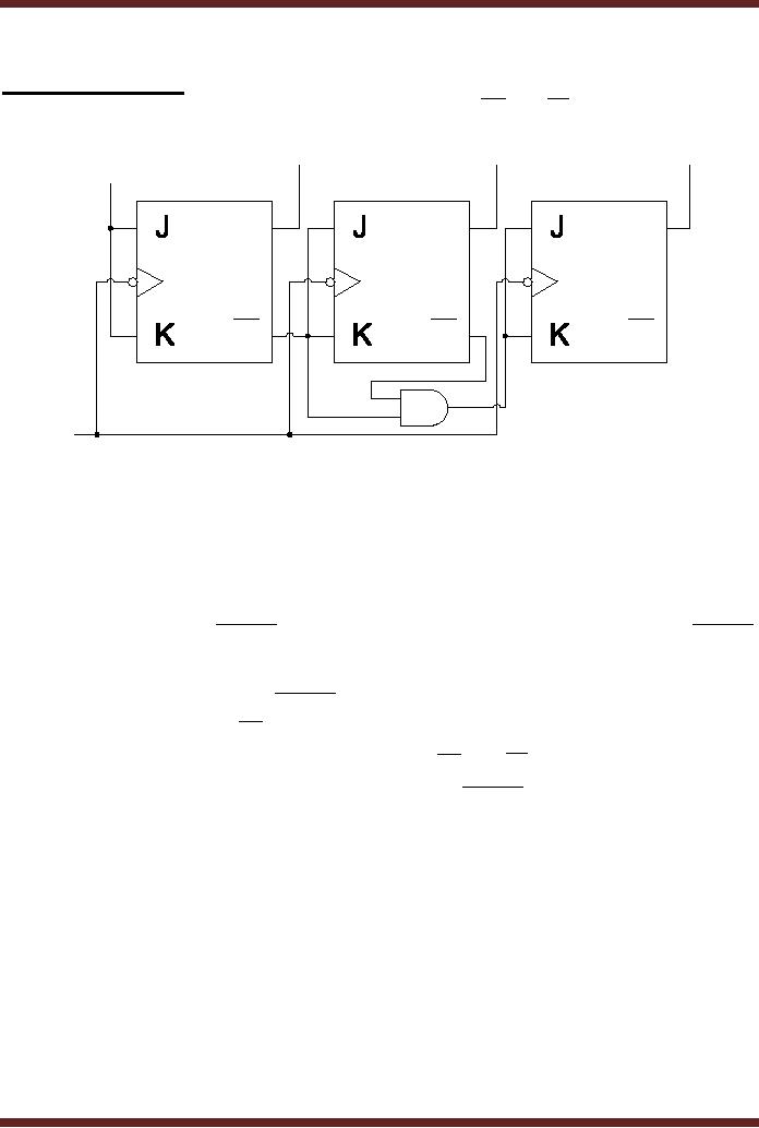
The
down-counter is implemented by connecting
the Q 0 and Q1
outputs.
Figure 29.1
F0
F1
F2
1
SET
SET
SET
Q
Q
Q
flip-flop
1
flip-flop
2
flip-flop
3
Q
Q
Q
CLR
CLR
CLR
CLK
Figure
29.1
3-bit
Synchronous Down-counter
The
down-counter counter circuit is
very similar to the
up-counter circuit
discussed
earlier.
The only change is the
connection of the AND gate to
the complementary outputs
of
the
first and second
flip-flops.
The
up-counter and down-counter
can be implemented as a single
counter circuit by
adding
some
extra logic. In the circuit
diagram, the Up-down counter
is configured to count up or
down by
setting the UP / DOWN input to logic 1 or 0
respectively. When the UP / DOWN
input is
set to logic 1, upper AND
gates are enabled, allowing
flip-flip 2 to toggle its
state when
F0 output of flip-flop 1 is
logic 1. Similarly when both
F0 and F1 outputs are logic 1,
flip-flop 3
toggles
its state. When the
UP / DOWN input is set to
logic 0, the lower AND gates
are
enabled.
When F0 is logic 0, Q 0 is logic 1
and the flip-flop 2 toggles
its output state.
Similarly,
when
both outputs F0 and
F1 are at logic 0,
that is, Q 0 and Q1 are at
logic 1 the flip-flop
3
toggles
its state. During the
counting sequence, the UP / DOWN input can be
set to logic 1 or
0 at any
time to reverse the counting
sequence. Figure 29.2
293
CS302 -
Digital Logic & Design
F0
F1
F2
UP / DOW
N
1
SET
SET
SET
J
Q
J
Q
J
Q
flip-flop
2
flip-flop
1
flip-flop
3
K
Q
K
Q
K
Q
CLR
CLR
CLR
CLK
Figure
29.2a Up-Down Synchronous
Counter
UP / DOWN
Figure
29.2b Timing diagram of an
Up-Down Synchronous
Counter
294
CS302 -
Digital Logic & Design
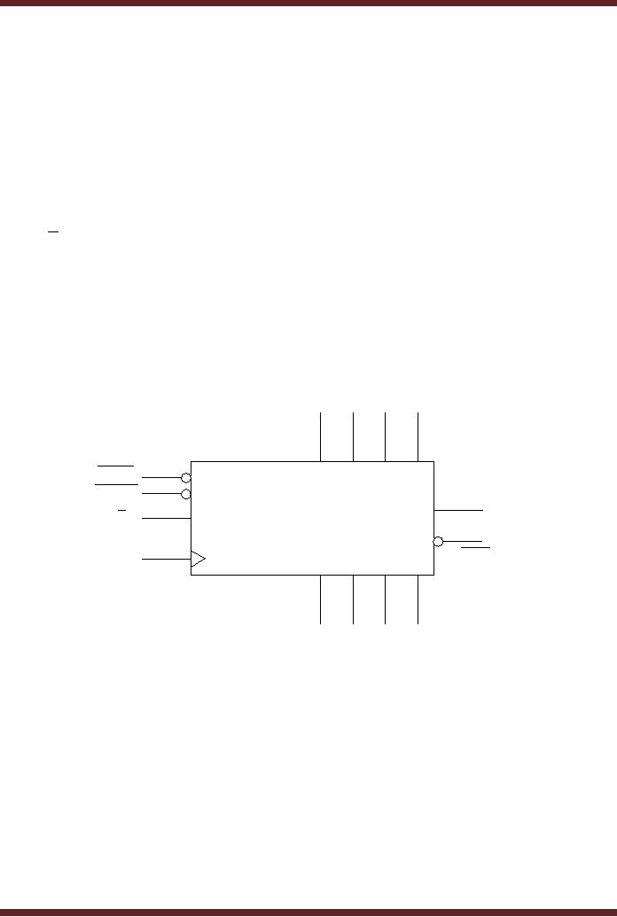
Integrated
Circuit Up/Down Decade
Counter
Implementing a
4-bit Up/Down counter by
connecting flip-flops and
logic gates
increases
the circuit size and
requires many connections.
The 74HC190 is a 4-bit
Up/Down
Synchronous
Counter available in an Integrated
Circuit form. Figure 29.3.
The counter has
the
following
pins.
1.
Parallel
data inputs D0, D1, D2 and D3
2.
Data
outputs Q0, Q1, Q2 and Q3
3.
Positive
edge-triggered CLOCK
signal
4.
Active-low
LOAD input which loads
the 4-bit data applied at
the counter inputs
5.
Active-low
CTEN counter enable
input
D / U the count
down/up input. When the
input is set to logic 1, the
counter counts down
6.
and
when the input is set to
logic 0, the counter counts
up
7. The MAX/MIN
output that is set to high
when the terminal count
1001 is reached when
counting up or
when the terminal count
0000 is reached when
counting down. The
MAX/MIN output
is logic high for one
complete cycle when a
terminal count is
reached.
8. The
Ripple Clock Output RCO
goes low when the
Counter reaches the terminal
count
1001 or
0000 when counting up or
down respectively. The RCO
output remains low
during
the
negative half of the clock
cycle. The RCO, the MAX/MIN
output along with CTEN
input
is used to
cascade multiple counter ICs
for implementing larger
counters.
D0 D1 D2 D3
CTEN
LOAD
MAX/MIN
74HC190
D/U
RCO
CLK
Q0 Q1 Q2 Q3
Figure
29.3
74HC190
4-bit Synchronous Up/Down
Counter
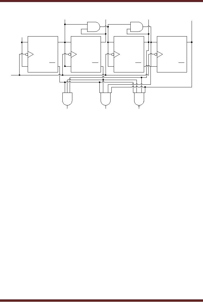
Counter
Decoding
In digital
circuits the counter outputs
are decoded using decoders
or logic gates to
determine
when the counter is in a
certain state in its
counting sequence. For
example, a 4-bit
Modulus-16
counter counts from state 0
to state 15. A digital
circuit is enabled when the
count
reaches
count value 4, a second
circuit is enabled when the
count value reaches 8 and a
third
circuit is
enabled when the count
value reaches 12. A decoder
using AND or NAND gates
logic
gates can be implemented.
Figure 29.4
295
CS302 -
Digital Logic & Design
F1
F2
F0
F3
1
SET
SET
SET
SET
J
Q
J
Q
J
Q
Q
J
flip-flop
1
flip-flop
2
flip-flop
3
flip-flop
4
K
Q
K
Q
K
Q
Q
K
CLR
CLR
CLR
CLR
CLK
Active-high
Active-high
Active-low
select
4
select
8
select
12
Figure
29.4a Decoder circuit
decoding counter outputs 4, 8
and 12
The
output of the first AND gate
is set to logic high when
the counter output is set
to
0100
(4). The output of the
second AND gate is set to
logic high when the
counter output is set
to 1000
(8). The NAND gate is set to
logic low when the
counter output is set to
1100 (12). The
propagation
delay due to ripple effect
in Asynchronous counters, discussed
earlier causes
these
Asynchronous counters to work
erratically. The propagation
problem also exists
in
Synchronous
counters to some degree due
to the propagation delays
from the clock
transition
to the Q
output of the flip-flop
which varies slightly for
each flip-flop. The timing
diagram for the
decoder
circuit shows that the
decoder outputs are
activated for different time
intervals at
different
intervals which are not in a
proper sequence. Figure
29.4b. The counter output
for
count 2 is
detected by the AND gate
decoder during interval t2A to t3 and again
for a very short
interval at
t4. Similarly, the
counter output 8 is selected
for a very short duration
between
intervals
tAB and t9. The decoder outputs
for very short durations at
interval t2, t4, t6 and t8 are
known as
`gliches'.
Glitches
can be eliminated by enabling
the decoder outputs after
the glitches have
settled
down. Glitches are removed
by using the clock signal to
enable the decoder
circuit.
Figure
29.5. The clock signal is
connected to the inputs of
each of the three decoder
gates.
During
the second, positive half of
the clock signal the
three gates are enabled,
all the glitches
occur
during the first negative
half of the clock cycle
during which the decoder
gates are
disabled.
This method is known as
Strobing method where the
decoder outputs are
activated
after
some delay allowing the
glitches to settle
down.
296
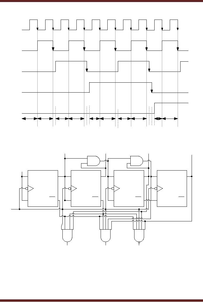
CS302 -
Digital Logic & Design
CLOCK
Input
F0
Output
F1
Output
F2
Output
F3
Output
0
1
0
2
3
20 4
5
4
6
7
640
9
t2 t2A
t3
t4 t4A t5
t6
t7
t8 tA8 t9
t10
t1
Figure
29.4b Decoded Outputs of
Synchronous Counter
F1
F2
F0
F3
1
SET
SET
SET
SET
J
Q
J
Q
J
Q
Q
J
flip-flop
1
flip-flop
2
flip-flop
3
flip-flop
4
K
Q
K
Q
K
Q
Q
K
CLR
CLR
CLR
CLR
CLK
Active-high
Active-high
Active-low
select
4
select
8
select
12
Figure
29.5
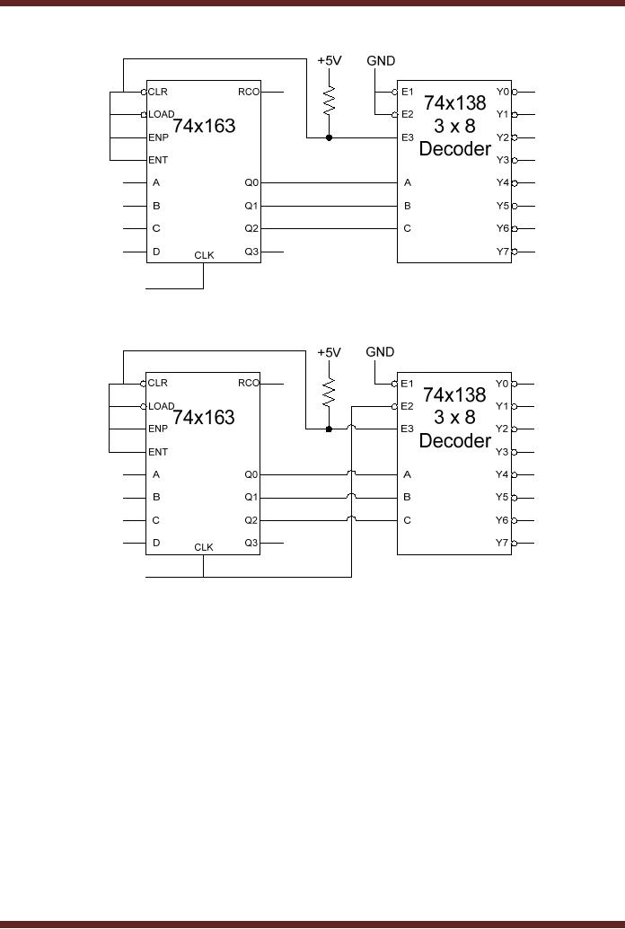
The
Decoder circuit connected to
remove glitches
Glitches
occur even with Integrated
circuits due to different
propagation delays
between
the clock transition and
the variable path lengths
between different inputs and
outputs
within
the integrated circuit. The
Glitches that occur at the
output of a 74x 138 3-to-8
decoder
connected to a
74HC163 counter can be
removed by enabling the
decoder during the
second
half of
the clock signal. Figure
29.6
297
CS302 -
Digital Logic & Design
Figure
29.6
74x163
Counter output Decoded using
a 3 x 8, 74x138 Decoder
Figure
29.7
74x138
Decoder enabled by a clock
signal
Counter
Applications
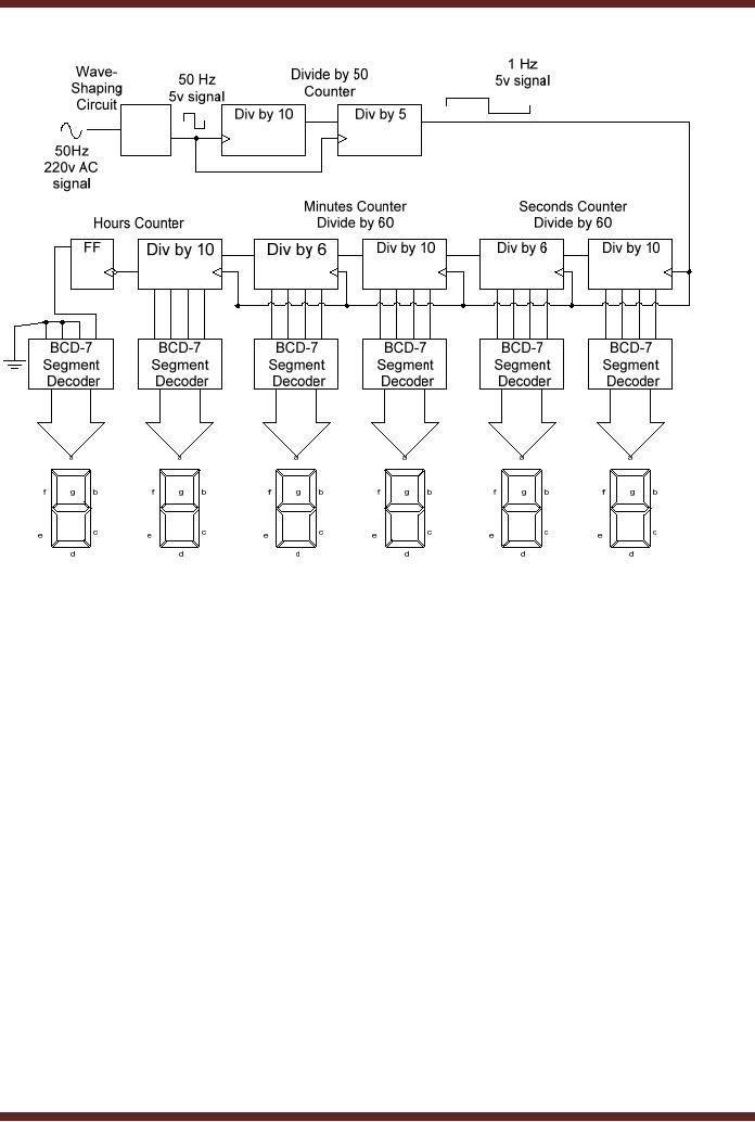
1. Digital
Clock
The
primary use of counter is in
counting applications and
sequencing through a set
of
operations. A
digital clock can be
implemented using the AC 50 Hz
frequency as the
clock
signal.
Figure 29.8
In the
digital clock circuit the 50
Hz, 220 volt ac mains
sinusoidal signal is shaped
into
a 50 Hz, 5
volt square-wave signal. A
divide-by-50 counter divides
the input 50 Hz signal to
a
1 Hz signal.
The Seconds, divide-by-60
counter counts up to sixty
seconds (0 to 59).
The
Minutes,
divide-by-60 counter also
counts up to sixty minutes
(0-59). The Hours,
decade
counter
counts from 0 to 9. The
flip-flop connected to the
output of the decade counter
is set to
0 or 1 to
represent hours from 0 to 9
and 10 to 12 respectively.
298
CS302 -
Digital Logic & Design
Figure
29.8
Digital
Clock Circuit
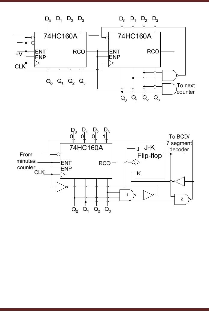
The
circuit diagram of the
Divide by 60 Seconds and
Minutes counter is shown in
figure
29.9.
The 74HC160A decade counter
is sued which has
Asynchronous clear. The
divide by 60
counter is
implemented by cascading two
74HC160A counters. The least
significant counter
which is
the units counter is
configured as a decade counter
and counts from 0000 to
1001.
On reaching
the terminal count value,
the RCO output of the
Units counter is set to high
which
enables
the tens counter. The
tens counter is configured as a
Mod-6 counter, thus it
counts
from
000 to 101. The NAND gate
output is set to low when
the counter counts up to
110, the
NAND gate
output is connected to the
asynchronous clear input
which resets the counter
to
000.
When the tens counter
reaches its terminal count
101, and the units
counter reaches its
terminal
count 1001, the AND gate
output is set to logic high
to indicate the terminal
count 59
of the
divide by 60 counter. The
output of the AND gate is
connected to the counter
enable
pins
ENT and ENP of the
next stage, thus on reaching
the terminal count the
next stage is
enabled
and the count is incremented
by 1 on a clock transition.
The
hours counter is implemented
using a single decade
counter and a flip-flop.
Two
counters
are not required as the
hours counter counts 12
unique output states.
Implementation
of a Mod-12
requires 5 flip-flops. Figure
29.10
299
CS302 -
Digital Logic & Design
CLR
CLR
LD
Figure
29.9
Divide by 60
Minutes and Seconds
counter
LD
Figure
29.10a Hours Counter
Circuit
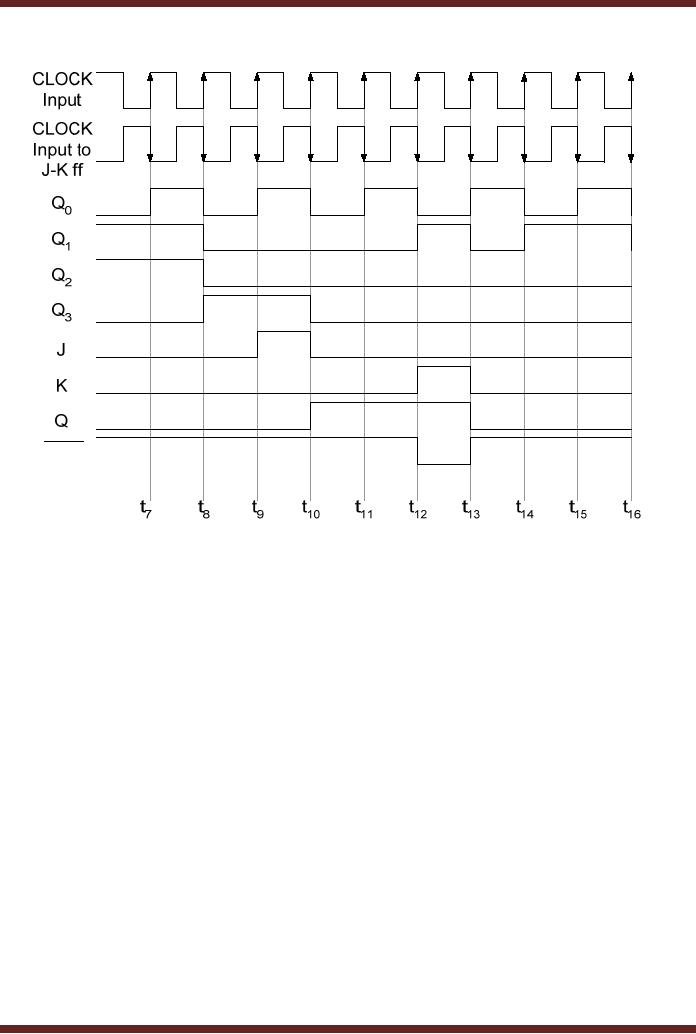
The
hours unit counter circuit
is configured as a decade counter,
counting from 0000 to
1001
when it is enabled by the
Minutes counter circuit. The
terminal count 1001 is
detected by
the NAND
gate (1) which sets
the J input of the flip-flop
to logic 1. The K input of
the flip-flop is
at Logic 0,
therefore on a clock transition
the JK flip-flop output is
set to logic 1 when the
units
counter
recycles to 0000. The NOT
gate connected to the clock
input of the J-K flip-flop
allows
the
J-K flip-flop to trigger
when the units counter is
triggered to count from 1001
to 0000. The
unit
counter counts to 0001 and
0010 to represent hours 11
and 12 respectively along
with the
output of
the J-K flip-flop which is
set to logic 1. On the next
clock transition when the
units
counter
counts to 0011 the NAND gate
(2) output set to logic 0
reloads the units counter
with
the
count value 0001 and
the J-K flip-flop toggles to
0 output as its K input
which is set to logic
1.
300
CS302 -
Digital Logic & Design
LOAD
Figure
29.10b Hours Counter timing
diagram
2. Frequency
Counter
A frequency
counter is used to measure
the frequency of an input
signal. The basis
for
the
operation of a frequency counter is
counting of the clock pulses
in predetermined time
interval.
The frequency of periodic
signal is the number of
cycles in a time period of
one
second.
The frequency of the unknown
signal can be calculated by
counting the number
of
clock
pulses of the unknown signal
and dividing the count
number by the time interval
in which
the
clock pulses are counted,
Figure 29.11
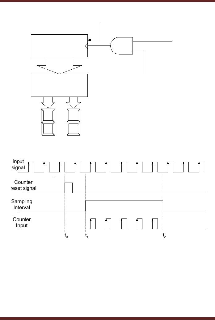
In the
circuit shown, the input
signal with unknown
frequency is applied at the
AND
gate
input. The second input of
the AND gate is connected to a
signal which determines
the
sampling
interval. The signal is set
to logic high at interval t1 to enable the AND gate
allowing
the
input signal to be connected to
the clock input of the
counter circuit. The
sampling interval
signal is
set to logic low at the
end of the sampling interval
t2 to disable the AND
gate and
inhibit
the counter from counting.
Before the counter counts
the clock pulses of the
input signal
it is reset by
activating the Asynchronous
input to clear the counter
at interval t0. At
the end of
the
sampling interval the
counter output is displayed on
7-segment displays.
301
CS302 -
Digital Logic & Design
Clear
Input
Signal with
unknown
frequency
Counter
Sampling
BCD &
Segment
Interval
Decoder
a
a
g
g
f
f
b
b
c
c
e
e
d
d
Figure
29.11a Frequency Counter
Circuit
Figure
29.11b Timing diagram of the
Frequency Counter
Circuit
The
accuracy of the frequency
counter depends on the
duration of the timing
sampling
interval,
which must be very accurate.
Consider that during a
sampling interval of 1
second
4573
clock pulses of the input
signal are measured. Thus,
the frequency of the unknown
signal
is 4573
Hz. If the same input
signal is sampled using a
0.1 second sampling interval
then
457.3
pulses are counted, which
means that either 457 or
458 will be counted
depending on
the
start of the sampling
interval at t1.
Similarly, if the sampling
interval is reduced to
0.01
seconds,
the numbers of clock pulses
measured are 45.73, which
means that either 45 or
46
will be
read.
302
CS302 -
Digital Logic & Design
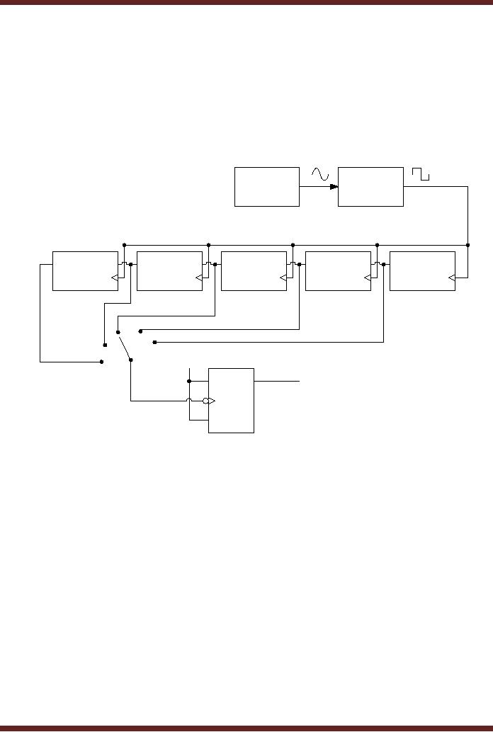
Very
accurate sampling intervals
are implemented using
cascaded counter which
is
connected to a
very accurate timing signal
generated by a crystal controlled
oscillator (Astable
multi-vibrator).
The output timing signal of
each cascade section is
available at a switch
which
is used to
select the appropriate
timing signal for
controlling the sampling
interval. The output
of the
switch is connected to the
clock input of a negative
triggered J-K flip-flop,
which divides
the
input signal by 2. Thus,
when the 1 Hz sampling
interval is selected, the
signal at the
output of
the J-K flip-flop has a
time period of 2 seconds.
Figure 29.12
100
100
KHz
KHz
Pulse
Crystal
Shaper
Oscillator
Div by
10
Div by
10
Div by
10
Div by
10
Div by
10
100
10
1
10
Hz
Hz
KHz
KHz
1
1
Divide
by
J
Q
Hz
2
output
K
Figure
29.12 Cascaded Counter
circuit for obtaining
accurate sampling
intervals
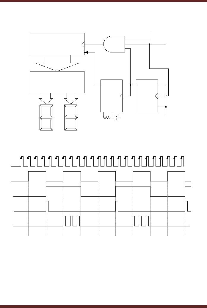
The
detailed circuit diagram and
the timing diagram of the
frequency diagram are
shown in
figure 29.13. In the timing
diagram the Sampling
Interval pulse is obtained
from the
output of
the J-K flip-flop shown in
figure 29.8. The duration of
the Sampling interval pulse
can
be selected
through the switch. The
sampling interval signal is
connected to the input of
the 3-
input AND
gate and the clock
input of the second J-K
flip-flop which toggles its
output at each
negative
transition of the clock.
When the output of the
second flip-flop changes to
logic 1
(interval
t1) it triggers the
One-Shot which generates a
short output pulse which
clears the
Counter
circuit. At interval t2 during the positive
half of the sampling
interval when the output
of
the
second J-K flip-flop is high
the 3-input AND gate is
enabled and the input
signal with
unknown
frequency is applied at the
input of the counter, which
count the input signal
pulses.
At interval
t3 there is
negative transition of the
sampling signal, which
triggers the second
flip-
flop
changing its output to logic
0. Logic 0 output of the
flip-flop disables the
3-input AND gate
inhibiting
the counter from counting.
The pulses counted by the
counter during interval t2 to t3
are
directly displayed.
303
CS302 -
Digital Logic & Design
Input
Signal with
unknown
frequency
Counter
Sampling
Clear
Interval
BCD &
Segment
Decoder
Q
Q
J
One
Flip-flop
Shot
2
a
a
K
g
g
f
f
b
b
1
c
c
e
e
d
d
Figure
29.13a Detailed circuit
diagram of a frequency
counter
Input
signal
Sampling
Interval
Output
of
flip-flop
2
Counter
reset
signal
Counter
Input
t0
t1
t2
t3
t4
t5
t6
t7
t8
t9
Figure
29.13b Timing diagram of the
frequency counter
circuit
Design of
Synchronous Counters
The
counters that have been
discussed are binary
counters that count in a
sequence
either
upwards or downwards. The
count start and end
sequence of a counter can
also be set
arbitrarily
and the counter can
then count up or down with
in the terminal count
limits.
Counters
can also be designed that do
not count in a sequence,
instead they sequence
304
CS302 -
Digital Logic & Design
through a
set of predefined arbitrary
values. Counters can also be
implemented using D
flip-
flops
instead of J-K flip-flops.
Counters are sequential
circuits which are designed
using
standard
set of steps.
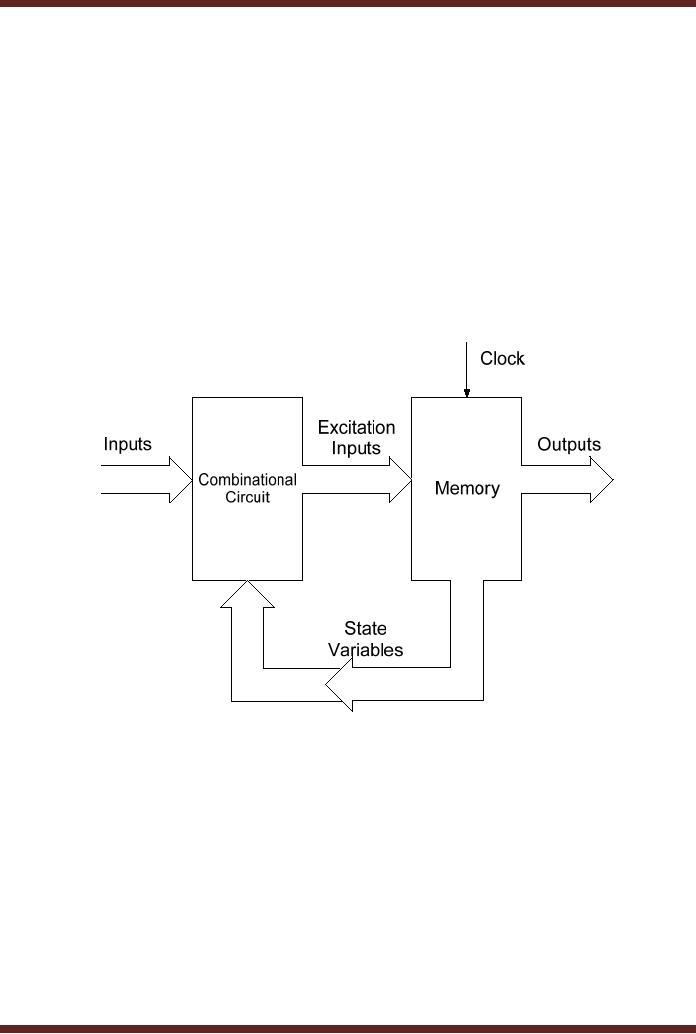
Sequential
Circuit (State
Machine)
A general
Sequential circuit consists of a
combinational circuit and a
memory circuit
(flip-flop). In
a clocked Sequential circuit
the memory element has a
clock input. At any
given
instant
the memory element is in its
present state. On a clock
transition the output of
the
memory
element changes to the next
state. The next state is
determined by the inputs
applied
at the
memory input at the time of
clock transition. The inputs
to the memory which allow
the
memory to
change its state on a clock
transition are known as
excitation inputs or
excitation
variables.
The present state of the
memory is represented by state
variables. The state
variables
and the inputs to the
sequential circuit determine
the sequential circuit
output. Figure
29.14
Figure
29.14 Clocked Sequential
Circuit Block diagram
Design
Procedure
The
design procedure is based on a
number of steps starting
from defining the
state
diagram
and ending at the
implementation of State
machine.
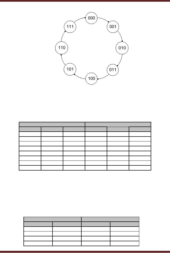
1. State
Diagram
A sequential
circuit (state machine) is
described by a state diagram,
which shows the
sequence of
state through which the
sequential circuit progresses
when it is clocked. The
state
diagram of a
3-bit Synchronous Up-Counter
(sequential circuit) is shown in
the figure.
28.3
305
CS302 -
Digital Logic & Design
Figure
28.3
State
diagram of a 3-bit
Up-Counter
2. Next-State
Table
Once
the state diagram of the
sequential circuit is defined, a
Next-State Table is
derived
which lists each present
state and the corresponding
next state. The next
state is the
state to
which the sequential circuit
switches when a clock
transition occurs. Table
28.1
Present
State
Next
State
Q2
Q1
Q0
Q2
Q1
Q0
0
0
0
0
0
1
0
0
1
0
1
0
0
1
0
0
1
1
0
1
1
1
0
0
1
0
0
1
0
1
1
0
1
1
1
0
1
1
0
1
1
1
1
1
1
0
0
0
Table
28.1
Next-State
Table for a 3-bit
Up-Counter
3. Flip-flop
Transition Table
The
Memory element of the
Sequential circuit is implemented
using flip-flops. The
number of
flip-flops used is determined by
the total number of states.
When there is a clock
transition at
the clock input of the
flip-flops they change from
their present state to the
next
state.
The Flip-flop transition
table lists all the
possible flip-flop input
combinations which
allows
the present state to change
to the next state on a
clock transition. The
flip-flop
transition
table is based on the
flip-flop used (D, S-R or
J-K). Table
28.2
Flip-flop
Inputs
Output
Transitions
J
K
Qt
Qt+1
0
x
0
0
1
x
0
1
x
1
1
0
x
0
1
1
306
CS302 -
Digital Logic & Design
Table
28.2
J-K
flip-flop Transition
table
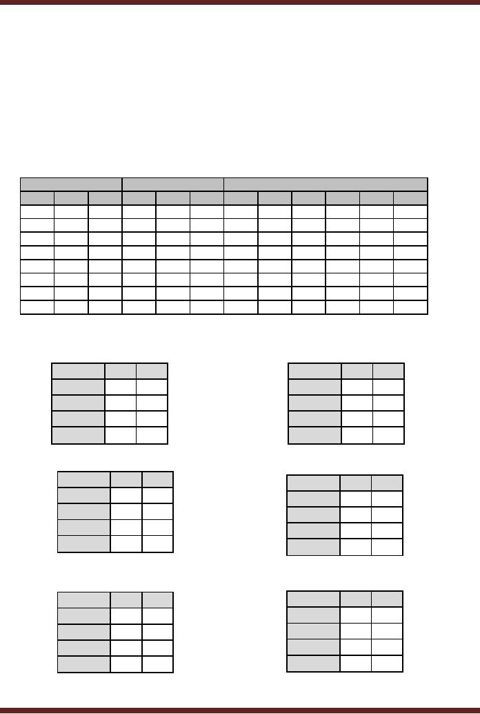
4. Karnaugh
Maps
For
each state variable shown in
the Next-State table, the
change from present state
to
the
next state on a clock
transition depends upon the
J-K inputs. Table
28.3. Considering
the
state
variable Q2, J2 and K2
inputs
set to 0 and x (don't care)
allow Q2
to change
from present
state 0 to
next state 0 shown in the
first row. Similarly, the
state variable Q0 changes from 1 to
0 when
J0 and K0 inputs are set at x
(don't care) and 1
respectively. The table is
completed
using
the information in the
Next-State table and the
J-K flip-flop transition
table. The J-K
inputs
can be directly mapped to
Karnaugh maps. Table
28.4
Present
State
Next
State
J-K
flip-flop inputs
Q2
Q1
Q0
Q2
Q1
Q0
J2
K2
J1
K1
J0
K0
0
0
0
0
0
1
0
x
0
x
1
x
0
0
1
0
1
0
0
x
1
x
x
1
0
1
0
0
1
1
0
x
x
0
1
x
0
1
1
1
0
0
1
x
x
1
x
1
1
0
0
1
0
1
x
0
0
x
1
x
1
0
1
1
1
0
x
0
1
x
x
1
1
1
0
1
1
1
x
0
x
0
1
x
1
1
1
0
0
0
x
1
x
1
x
1
Table
28.3
J-K
flip-flop input table
Q2Q1/Q0
0
1
Q2Q1/Q0
0
1
00
0
0
00
x
x
01
0
1
01
x
x
11
x
x
11
0
1
10
x
x
10
0
0
Table
28.4a
Karnaugh Map
for J2
and
K2 inputs
Q2Q1/Q0
0
1
Q2Q1/Q0
0
1
00
0
1
00
x
x
01
x
X
01
0
1
11
x
X
11
0
1
10
0
1
10
x
x
Karnaugh Map
for J1
and
K1 inputs
Table
28.4b
Q2Q1/Q0
0
1
Q2Q1/Q0
0
1
00
x
1
00
1
x
01
x
1
01
1
x
11
x
1
11
1
x
10
x
1
10
1
x
Table
28.4c
Karnaugh Map
for J0
and
K0 inputs
307
CS302 -
Digital Logic & Design
5. Logic
expressions for Flip-flop
Inputs
Simplified
expressions for J2-K2, J1-K1 and
J0-K0 are
directly obtained from
the
Karnaugh
maps.
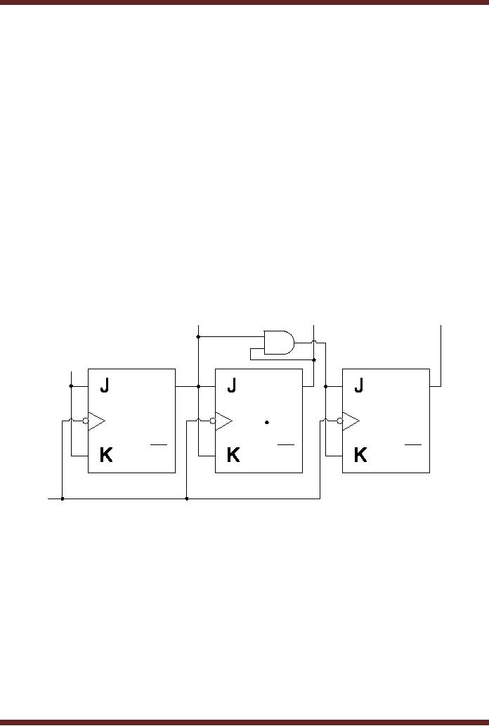
J2 = Q1Q 0
K 2 = Q1Q 0
J1 = Q 0
K1 = Q0
J0 = 1
K0 = 1
6. Sequential
Circuit Implementation
The
Boolean expressions obtained in
the previous step are
implemented using
logic
gates.
The sequential circuit
implemented is shown in figure
28.4.
Q0
Q1
Q2
1
SET
SET
SET
Q
Q
Q
flip-flop
1
flip-flop
2
flip-flop
3
Q
Q
Q
CLR
CLR
CLR
CLK
Figure
28.4
Implementation
of the Sequential
Circuit
Implementing a
3-bit Up/Down
Counter
1. State
Diagram
The
state diagram of a 3-bit
Up/Down Synchronous Counter is
shown in the figure.
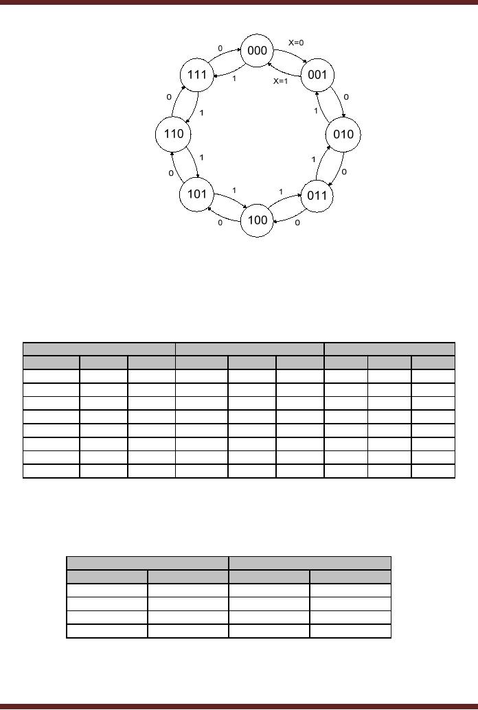
28.5. X=0
and X =1 indicates that the
counter counts up when input
X = 0 and it counts
down
when X
=1.
308
CS302 -
Digital Logic & Design
Figure
28.5
State
diagram of a 3-bit
Up-Counter
2. Next-State
Table
The
next state is the state to
which the sequential circuit
switches when a clock
transition
occurs. Table
28.5. The
next state outputs for
X=0 and X=1 are
shown separately.
Present
State
Next
State X=0
Next
State X=1
Q2
Q1
Q0
Q2
Q1
Q0
Q2
Q1
Q0
0
0
0
0
0
1
1
1
1
0
0
1
0
1
0
0
0
0
0
1
0
0
1
1
0
0
1
0
1
1
1
0
0
0
1
0
1
0
0
1
0
1
0
1
1
1
0
1
1
1
0
1
0
0
1
1
0
1
1
1
1
0
1
1
1
1
0
0
0
1
1
0
Table
28.5
Next-State
Table for a 3-bit
Up-Counter
3. Flip-flop
Transition Table
The
flip-flop transition table is
based on the J-K flip-flop.
Table
28.6
Flip-flop
Inputs
Output
Transitions
J
K
Qt
Qt+1
0
x
0
0
1
x
0
1
x
1
1
0
x
0
1
1
Table
28.6
J-K
flip-flop Transition
table
309
CS302 -
Digital Logic & Design
4. Karnaugh
Maps
The
J-K flip-flop inputs for
change in state variables
when X=0 and X=1
are shown in
the
table
28.7. The
J-K inputs can be directly
mapped to 4-Variable Karnaugh
maps. Table
28.8.
Present
State
Next
State X=0
J-K
flip-flop inputs
Q2
Q1
Q0
Q2
Q1
Q0
J2
K2
J1
K1
J0
K0
0
0
0
0
0
1
0
x
0
x
1
x
0
0
1
0
1
0
0
x
1
x
x
1
0
1
0
0
1
1
0
x
x
0
1
x
0
1
1
1
0
0
1
x
x
1
x
1
1
0
0
1
0
1
x
0
0
x
1
x
1
0
1
1
1
0
x
0
1
x
x
1
1
1
0
1
1
1
x
0
x
0
1
x
1
1
1
0
0
0
x
1
x
1
x
1
Table
28.7a
J-K
flip-flop input table for
X=0
Present
State
Next
State X=1
J-K
flip-flop inputs
Q2
Q1
Q0
Q2
Q1
Q0
J2
K2
J1
K1
J0
K0
0
0
0
1
1
1
1
x
1
x
1
x
0
0
1
0
0
0
0
x
0
x
x
1
0
1
0
0
0
1
0
x
x
1
1
x
0
1
1
0
1
0
0
x
x
0
x
1
1
0
0
0
1
1
x
1
1
x
1
x
1
0
1
1
0
0
x
0
0
x
x
1
1
1
0
1
0
1
x
0
x
1
1
x
1
1
1
1
1
0
x
0
x
0
x
1
Table
28.7b
J-K
flip-flop input table for
X=1
Q2Q1/Q0X
00
01
11
10
Q2Q1/Q0X
00
01
11
10
00
x
x
x
x
00
0
1
0
0
01
x
x
x
x
01
0
0
0
1
11
0
0
0
1
11
x
x
x
x
10
0
1
0
0
10
x
x
x
x
Table
28.8a
Karnaugh Map
for J2
and
K2 inputs
Q2Q1/Q0X
00
01
11
10
Q2Q1/Q0X
00
01
11
10
00
0
1
0
1
00
x
x
x
x
01
x
x
x
x
01
0
1
0
1
11
x
x
x
x
11
0
1
0
1
10
0
1
0
1
10
x
x
x
x
Table
28.8b
Karnaugh Map
for J1
and
K1 inputs
310
CS302 -
Digital Logic & Design
Q2Q1/Q0X
00
01
11
10
Q2Q1/Q0X
00
01
11
10
00
x
x
1
1
00
1
1
x
x
01
x
x
1
1
01
1
1
x
x
11
x
x
1
1
11
1
1
x
x
10
x
x
1
1
10
1
1
x
x
Table
28.8c
Karnaugh Map
for J0
and
K0 inputs
5. Logic
expressions for Flip-flop
Inputs
Simplified
expressions for J2-K2, J1-K1 and J0-K0 are directly obtained
from the
Karnaugh
maps.
J2 = Q1Q 0 X + Q1 Q 0 X
K 2 = Q1Q 0 X + Q1 Q 0 X
J1 = Q 0 X + Q 0 X
K1 = Q0 X + Q0 X
J0 = 1
K0 = 1
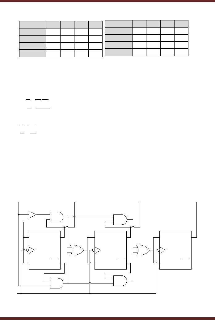
6. Sequential
Circuit Implementation
The
Boolean expressions obtained in
the previous step are
implemented using
logic
gates.
The sequential circuit
implemented is shown in figure
28.6.
X=0
(up)
Q0
Q1
Q2
X=1
(down)
1
SET
SET
SET
J
Q
J
Q
J
Q
flip-flop
2
flip-flop
1
flip-flop
3
K
Q
K
Q
K
Q
CLR
CLR
CLR
CLK
Figure
28.6
Implementation
of the Sequential
Circuit
311
Table of Contents:
- AN OVERVIEW & NUMBER SYSTEMS
- Binary to Decimal to Binary conversion, Binary Arithmetic, 1s & 2s complement
- Range of Numbers and Overflow, Floating-Point, Hexadecimal Numbers
- Octal Numbers, Octal to Binary Decimal to Octal Conversion
- LOGIC GATES: AND Gate, OR Gate, NOT Gate, NAND Gate
- AND OR NAND XOR XNOR Gate Implementation and Applications
- DC Supply Voltage, TTL Logic Levels, Noise Margin, Power Dissipation
- Boolean Addition, Multiplication, Commutative Law, Associative Law, Distributive Law, Demorgans Theorems
- Simplification of Boolean Expression, Standard POS form, Minterms and Maxterms
- KARNAUGH MAP, Mapping a non-standard SOP Expression
- Converting between POS and SOP using the K-map
- COMPARATOR: Quine-McCluskey Simplification Method
- ODD-PRIME NUMBER DETECTOR, Combinational Circuit Implementation
- IMPLEMENTATION OF AN ODD-PARITY GENERATOR CIRCUIT
- BCD ADDER: 2-digit BCD Adder, A 4-bit Adder Subtracter Unit
- 16-BIT ALU, MSI 4-bit Comparator, Decoders
- BCD to 7-Segment Decoder, Decimal-to-BCD Encoder
- 2-INPUT 4-BIT MULTIPLEXER, 8, 16-Input Multiplexer, Logic Function Generator
- Applications of Demultiplexer, PROM, PLA, PAL, GAL
- OLMC Combinational Mode, Tri-State Buffers, The GAL16V8, Introduction to ABEL
- OLMC for GAL16V8, Tri-state Buffer and OLMC output pin
- Implementation of Quad MUX, Latches and Flip-Flops
- APPLICATION OF S-R LATCH, Edge-Triggered D Flip-Flop, J-K Flip-flop
- Data Storage using D-flip-flop, Synchronizing Asynchronous inputs using D flip-flop
- Dual Positive-Edge triggered D flip-flop, J-K flip-flop, Master-Slave Flip-Flops
- THE 555 TIMER: Race Conditions, Asynchronous, Ripple Counters
- Down Counter with truncated sequence, 4-bit Synchronous Decade Counter
- Mod-n Synchronous Counter, Cascading Counters, Up-Down Counter
- Integrated Circuit Up Down Decade Counter Design and Applications
- DIGITAL CLOCK: Clocked Synchronous State Machines
- NEXT-STATE TABLE: Flip-flop Transition Table, Karnaugh Maps
- D FLIP-FLOP BASED IMPLEMENTATION
- Moore Machine State Diagram, Mealy Machine State Diagram, Karnaugh Maps
- SHIFT REGISTERS: Serial In/Shift Left,Right/Serial Out Operation
- APPLICATIONS OF SHIFT REGISTERS: Serial-to-Parallel Converter
- Elevator Control System: Elevator State Diagram, State Table, Input and Output Signals, Input Latches
- Traffic Signal Control System: Switching of Traffic Lights, Inputs and Outputs, State Machine
- Traffic Signal Control System: EQUATION DEFINITION
- Memory Organization, Capacity, Density, Signals and Basic Operations, Read, Write, Address, data Signals
- Memory Read, Write Cycle, Synchronous Burst SRAM, Dynamic RAM
- Burst, Distributed Refresh, Types of DRAMs, ROM Read-Only Memory, Mask ROM
- First In-First Out (FIFO) Memory
- LAST IN-FIRST OUT (LIFO) MEMORY
- THE LOGIC BLOCK: Analogue to Digital Conversion, Logic Element, Look-Up Table
- SUCCESSIVE APPROXIMATION ANALOGUE TO DIGITAL CONVERTER