 |
Implementation of Quad MUX, Latches and Flip-Flops |
| << OLMC for GAL16V8, Tri-state Buffer and OLMC output pin |
| APPLICATION OF S-R LATCH, Edge-Triggered D Flip-Flop, J-K Flip-flop >> |
CS302 -
Digital Logic & Design
Lesson
No. 22
ABEL
INPUT FILE OF A QUAD 1-OF-4
MUX
A Quad
1-of-4 MUX has four
Multiplexers, each Multiplexer
has four inputs and
a
single
output. Each multiplexer has
two select inputs to select
one of the four inputs.
The two
select
inputs are common to all
the four multiplexers. The
function table of the Quad
1-of-4
MUX is shown in
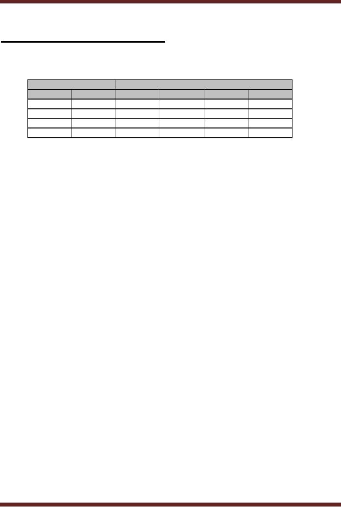
table 22.1.
Select
Inputs
Outputs
S1
S0
Dout
Cout
Bout
Aout
0
0
D0
C0
B0
A0
0
1
D1
C1
B1
A1
1
0
D2
C2
B2
A2
1
1
D3
C3
B3
A3
Table
22.1
Truth
table of a Quad 1-of-4
Multiplexer
Module
quad_1of4_mux
Title
`Quad 1 of 4
multiplexer in a GAL20V8'
mux
device
`P20V8';
A0,
A1, A2, A3
pin 1, 2, 3,
4;
B0,
B1, B2, B3
pin 5, 6, 7,
8;
C0,
C1, C2, C3
pin 9,
10, 11, 13;
D0,
D1, D2, D3
pin
14, 15, 16,
17;
Aout,
Bout, Cout, Dout
pin
21, 20, 19,
18;
S0,
S1
pin
22, 23;
Equations
Aout =
!S1 & !S0 & A0 # !S1 & S0
& A1 # S1& !S0 & A2 # S1 & S0 &
A3;
Bout =
!S1 & !S0 & B0 # !S1 & S0
& B1 # S1& !S0 & B2 # S1 & S0 &
B3;
Cout =
!S1 & !S0 & C0 # !S1 & S0
& C1 # S1& !S0 & C2 # S1 & S0 &
C3;
Dout =
!S1 & !S0 & D0 # !S1 & S0
& D1 # S1& !S0 & D2 # S1 & S0 &
D3;
Test_vectors
([S1,
S0, A0, A1, A2,
A3, B0, B1, B2,
B3, C0, C1, C2,
C3, D0, D1, D2,
D3] →
[Aout,
Bout, Cout, Dout])
"S S A A A A B B B B C C C C
D D D D outputs
"0 1 0 1 2 3 0 1 2 3 0 1 2 3
0 1 2 3
A B C D
[0,
0,
1,
0,
0,
0, 0,
1,
0, 0,
0,
0,
1, 0,
0,
0, 0,
1]
→
[1,
0,
0,
0];
[0,
1,
1,
0,
0,
0, 0,
1,
0, 0,
0,
0,
1, 0,
0,
0, 0,
1]
→
[0,
1,
0,
0];
[1,
0,
1,
0,
0,
0, 0,
1,
0, 0,
0,
0,
1, 0,
0,
0, 0,
1]
→
[0,
0,
1,
0];
[1,
1,
1,
0,
0,
0, 0,
1,
0, 0,
0,
0,
1, 0,
0,
0, 0,
1]
→
[0,
0,
0,
1];
[0,
0,
1,
1,
1,
0, 1,
1,
0, 1,
1,
0,
1, 1,
0,
1, 1,
1]
→
[1,
1,
1,
0];
[0,
1,
1,
1,
1,
0, 1,
1,
0, 1,
1,
0,
1, 1,
0,
1, 1,
1]
→
[1,
1,
0,
1];
[1,
0,
1,
1,
1,
0, 1,
1,
0, 1,
1,
0,
1, 1,
0,
1, 1,
1]
→
[1,
0,
1,
1];
[1,
1,
1,
1,
1,
0, 1,
1,
0, 1,
1,
0,
1, 1,
0,
1, 1,
1]
→
[0,
1,
1,
1];
END
Figure
22.1
ABEL
Input file for the
Quad 1-of-4 MUX
216
CS302 -
Digital Logic & Design
Implementation of
Quad MUX
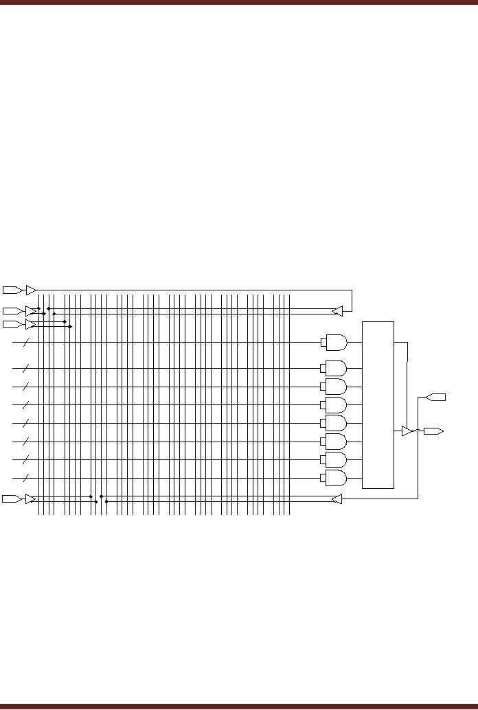
The
Quad Multiplexer has 16
inputs, 4 inputs for each
Multiplexer. Each
multiplexer
has a
single output, therefore a
total of 4 outputs are
required. To select an
appropriate
multiplexer
input there are two
select input lines connected
to all the four
multiplexers. The
Quad
Multiplexer has a total of 22
pins through which the
device is operated. The
GAL16V8
device
can not be used as it does
not enough pins to implement
the quad multiplexer.
The
GAL20V8
PLD is used for the
implementation of the Quad
1-of-4 Multiplexer. The
device has
12 inputs, 2
special function inputs and
8 input/output pins. Four
input/output pins of the
GAL
device
are configured as inputs to
support the fourth
multiplexer inputs D1, D2
and D3 and the
select
input S0.
Each
Multiplexer output Aout ,
Bout, Cout and Dout is
represented by a Sum-of-
product
Boolean expression, each
having four product terms.
Refer to figure 21.16. Thus
each
of the
four OLMCs which are
connected to the four output
pins have four product
terms
connected to
the inputs of the OR gates.
The implementation of the
multiplexer function
Aout
is shown in
figure 22.2.
Input
Lines
A0
A1
A0
A2
S1
A3
S0
B0
B1
B2
D3
B3
D2
C0
D1
C1
D0
C2
C3
A1
A2
x
x
x
32
x
x
x
32
xx
x
32
S0
x
x x
OLMC
32
32
Aout
32
32
32
A3
Figure
22.2
Implementation
of 1-of-4 Multiplexer
Sequential
Circuits
The
combinational digital circuits
have no storage element;
therefore combinational
circuits
handle only instantaneous
inputs. The outputs of the
combinational circuits also
can
not be
stored. The absence of a
memory element restricts the
use of digital
combinational
circuits to
certain application areas.
The use of a memory element
which is capable of
storing
digital
inputs and outputs is an
important part of all
practical digital
circuits.
Consider an ALU
which performs Arithmetic
and Logical operations. An ALU
can not
perform
its operations unless it is
connected to memory elements
that store the inputs
applied
at the
inputs of the ALU and
outputs from the ALU.
Consider an ALU that performs
addition
operation on a
set of numbers, 2, 3, 4 and 5.
The ALU can add two
numbers at a time;
217
CS302 -
Digital Logic & Design
therefore
the ALU has to add the
four numbers two at a time.
The four numbers have to
be
stored
temporarily, the partial
results after adding two
numbers also need to be
stored. To add
the
four numbers, the first
two numbers 2 and 3 stored
in two separate memory
elements are
added
together, the result (5)
has to be added to the next
number 4. The result (5)
is
temporarily
stored in one of the two
memory elements used to
store the numbers 2 and 3.
The
result
(5) is added to the third
number 4 to provide another
partial sum result 9 which
has to be
stored
and then added with
the fourth number 5.
In a
parallel-to-serial conversion of byte
data using a multiplexer and
the conversion
from
serial-to-parallel using a demultiplexer,
memory elements are required
that store the
byte
data at
the input of the multiplexer
for conversion into serial
information and another
memory
element at
the output of the
demultiplexer for conversion
back to parallel.
The
counter circuit used in
digital circuits count to
the next value because of
the
memory
element which stores and
remembers the previous count
value. A counter can
not
operate
without a memory
element.
Digital
circuits that use memory
elements for their operation
are known as
Sequential
circuits.
Thus Sequential circuits are
implemented by combining combinational
circuits with
memory
elements.
Latches
and Flip-Flops
A latch is a
temporary storage device
that has two stable
states. A latch output
can
change
from one state to the
other by applying appropriate
inputs. A latch normally has
two
inputs,
the binary input
combinations at the latch
input allows the latch to
change its state. A
latch
has two outputs Q and
its complement Q . The
latch is said to be in logic
high state when
Q=1
and Q =0 and it is in
the logic low state
when Q=0 and Q =1.
When the latch is set to
a
certain
state it retains its state
unless the inputs are
changed to set the latch to
a new state.
Thus a
latch is a memory element
which is able to retain the
information stored in
it.
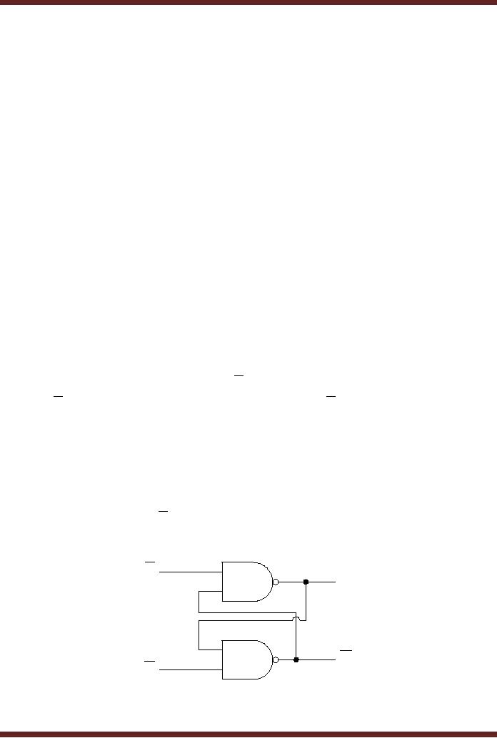
The
NAND gate based S-R
(Set-Reset) Latch
An S-R
Latch is implemented by connecting
two NAND gates together. The
output of
each NAND
gate is connected to the
input of the other NAND
gate. The unconnected inputs
of
the
two NAND gates are the
Set S and Reset R inputs.
The outputs of the two NAND
gates
are
the Q and its complement
Q . The
circuit diagram of the NAND
based S-R latch is shown
in
figure
22.3
S
Q
1
Q
2
R
Figure
22.3
NAND based
S-R Latch
218

CS302 -
Digital Logic & Design
The
S-R latch has two
inputs, therefore four
different combinations of inputs
can be
applied to
control the operation of the
S-R latch. The four
possible input combinations
are
1. Inputs
S=0 & R=0
a. Assume
that the outputs Q and
Q are
set at logic 1 and logic 0
respectively. Since
both
the
inputs S and R are logic
low, therefore both the Q
and Q outputs
are set to 1. The
inputs S = 0
and R = 0 are never applied
as these inputs result in
invalid output states as
Q
and Q should be
complements of each
other.
b. Assume
that the outputs Q and
Q are
set at logic 0 and logic 1
respectively. Since
both
the
inputs S and R are logic
low, therefore both the Q
and Q outputs
are set to 1. The
inputs S = 0
and R = 0 are never applied
as these inputs result in
invalid output states as
Q
and Q should be
complements of each
other.
The
input combination S=0 and
R=0 is considered to be invalid as it
results in an
invalid
output of Q=1 and Q =1.
2. Inputs
S=0 & R=1
a. Consider
that the outputs Q and
Q have 1
and 0 logic states. The
Set input S = 0 sets
the
output Q to 1.
The Q input and the R
inputs to gate 2 are both at
logic 1, therefore
the
output
Q is set to
0.
b. Consider
that initially the Q and
Q outputs
are at logic state 0 and 1
respectively. The Set
input S = 0
sets the output Q to 1. The
Q input and the R inputs to
gate 2 are both at
logic
1, therefore
the output Q is set to
0.
Thus
what ever the initial
outputs, setting S to 0 and R to 1
sets the Q and Q outputs
to 1 and 0
respectively.
3. Inputs
S=1 & R=0
a. Initially,
the Q and Q outputs
are at 1 and 0 respectively.
The Reset input R=0
sets the
output
Q to 1. The
inputs of gate 1, Q and S
are both at logic 1,
therefore the output Q
is
set to
0.
b. Initially, if
the Q and Q outputs
are at logic 0 and 1
respectively, setting R to 0 sets
Q to 1.
The
inputs of gate 1, Q and S
are both at logic 1,
therefore the output Q is
set to 0.
Thus,
what ever the outputs,
setting S to 1 and R to 0 sets
the Q and Q outputs to
0
and 1
respectively.
4. Inputs
S=1 & R=1
219
CS302 -
Digital Logic & Design
a. Initially,
the Q and Q
outputs
are at 1 and 0 respectively.
The inputs of gate 2 , Q and
R
are
both at logic 1, therefore
the output Q
is set to 0.
The inputs of gate 1, Q and S
are 0
and 1
respectively, therefore the
output is set to 1.
b. Initially,
the Q and Q outputs
are at 0 and 1 respectively.
The inputs of gate 2 , Q and
R
are at
logic 0 and 1 respectively,
therefore the output Q is set to 1.
The inputs of gate 1,
Q and S
are both at logic 1
respectively, therefore the
output is set to 0.
Thus,
with S and R inputs both
set to logic 1, the previous
output state is maintained.
If
initially,
the Q and Q are at
logic 1 and 0 respectively,
setting S=1 and R=1
maintains the same
outputs.
Similarly, if initially Q and
Q are at
logic 0 and 1 respectively,
setting S=1 and
R=1
maintains
the same outputs.
A truth-table
shows the operation of the
S-R NAND based latch. Table
22.2. The
Output
Qt+1 represents the Q
output of NAND gate 1 at time
interval t+1.When inputs are
S = 1
and R = 1
the next state output
Qt+1 remains the
same as the previous state
output Qt.
When
inputs
are S = 0 and R = 1 the
output Q is set to 1. When
inputs are S = 1 and R = 0
the output
Q is set to 0.
Inputs S = 0 and R = 0 are
not applied as they place
the latch in an invalid
state.
The NAND
gate based S-R latch
has active-low
inputs.
Input
Output
S
R
Qt+1
0
0
invalid
0
1
1
1
0
0
1
1
Qt
Table
22.2
Truth-Table of
NAND based S-R Latch
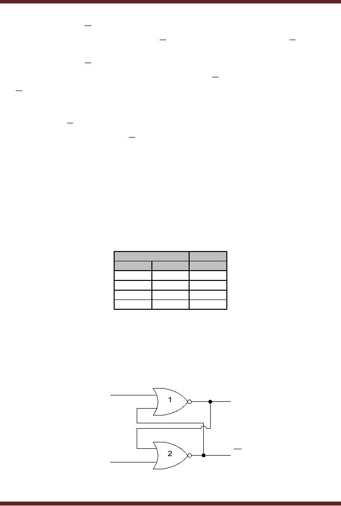
The
NOR gate based S-R
(Set-Reset) Latch
A NOR
based S-R latch is
implemented using NOR gates
instead of NAND gates.
Connections
are identical to that of the
NAND based latch. The S and
R inputs have been
switched.
Figure 22.2.
R
Q
Q
S
Figure
22.4
NOR
based S-R Latch
220

CS302 -
Digital Logic & Design
The
S-R NOR based latch
has two inputs, therefore
four different combinations
of
inputs
can be applied to control
the operation of the S-R
latch. The four possible
input
combinations
are
1. Inputs
S=0 & R=0
a. Assume
that the outputs Q and
Q are
set at logic 1 and logic 0
respectively. The R and Q
inputs at
gate 1 are both at logic 0,
therefore the Q output is
set to logic 1. The S and
Q
inputs at
gate 2 are at logic 0 and 1
respectively, therefore the
output Q is set to
logic 0.
b. Assume
that the outputs Q and
Q are
set at logic 0 and logic 1
respectively. The S and
Q
inputs at
gate 2 are both at logic 0,
therefore the Q output is
set to logic 1. The R and
Q
inputs at
gate 1 are at logic 0 and 1
respectively, therefore the
output Q is set to logic
0.
Thus,
with S and R inputs both
set to logic 0, the previous
output state is maintained.
If
initially,
the Q and Q are at
logic 1 and 0 respectively,
setting S=0 and R=0
maintains the same
outputs.
Similarly, if initially Q and
Q are at
logic 0 and 1 respectively,
setting S=0 and
R=0
maintains
the same outputs.
2. Inputs
S=0 & R=1
a. Consider
that the outputs Q and
Q have 1
and 0 logic states. The
Reset input R = 1
sets
the
output Q to 0. The Q input
and the S inputs to gate 2
are both at logic 0,
therefore the
output
Q is set to
1.
b. Consider
that initially the Q and
Q outputs
are at logic state 0 and 1
respectively. The
Reset
input R = 1 sets the output
Q to 0. The Q input and the
S inputs to gate 2 are both
at
logic 0,
therefore the output Q is set to
1.
Thus
what ever the initial
outputs, setting S to 0 and R to 1
sets the Q and Q outputs
to 0 and 1
respectively.
3. Inputs
S=1 & R=0
a. Initially,
the Q and Q outputs
are at 1 and 0 respectively.
The Set input S=1
sets the
output
Q to 0. The
inputs of gate 1, Q and R
are both at logic 0,
therefore the output Q
is
set to
1.
b. Initially, if
the Q and Q outputs
are at logic 0 and 1
respectively, setting S to 1 sets
Q to 0.
The
inputs of gate 1, Q and R
are both at logic 0,
therefore the output Q is
set to 1.
Thus,
what ever the outputs,
setting S to 1 and R to 0 sets
the Q and Q outputs to
1
and 0
respectively.
4. Inputs
S=1 & R=1
a. Initially,
the Q and Q outputs
are at 1 and 0 respectively.
Since both the inputs S
and R
are
logic 1, therefore both the
Q and Q outputs
are set to 0. The inputs S =
1 and R = 1
221
CS302 -
Digital Logic & Design
are
never applied as these
inputs result in invalid
output states as Q and Q should
be
complements of
each other.
b. Initially,
the Q and Q outputs
are at 0 and 1 respectively.
Since both the inputs S
and R
are
logic 1, therefore both the
Q and Q outputs
are set to 0. The inputs S =
1 and R = 1
are
never applied as these
inputs result in invalid
output states as Q and Q should
be
complements of
each other.
The
input combination S=1 and
R=1 is considered to be invalid as it
results in an
invalid
output of Q=0 and Q =0.
The
truth table of the NOR
gate based latch is shown.
Table 22.3. When inputs
are S =
0 and R = 0
the next state output
Qt+1 remains the
same as the previous state
output Qt.
When
inputs
are S = 0 and R = 1 the
output Q is set to 0. When
inputs are S = 1 and R = 0
the output
Q is set to 1.
Inputs S = 1 and R = 1 are
not applied as they place
the latch in an invalid
state.
The
NOR gate based S-R
latch has active-high
inputs.
Input
Output
S
R
Qt+1
0
0
Qt
0
1
0
1
0
1
1
1
invalid
Table
22.3
Truth-Table of
NOR based S-R
Latch
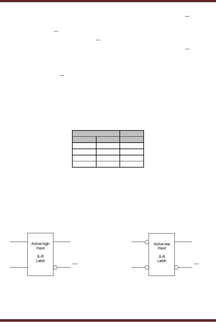
Comparing
the operation of the NOR
based and NAND based S-R
latches. The NAND
based
latch has active-low inputs,
where as NOR based latch
has active-high inputs. Both
the
S-R
latches are set to logic 1
when the set input is
activated and the reset
input is inactive.
Both
the latches are set to
logic 0 when the reset
input is activated and the
set input is
inactive.
The latches maintain the
output state when both
the set and reset
inputs are inactive.
For
both the latches both
the set and reset
inputs can not be activated
simultaneously as this
leads to
invalid output states. The
Logic symbols of the two
latches are shown in figure
22.5.
S
Q
S
Q
R
R
Q
Q
Figure
22.5
NOR
based Active-High and NAND
based Active-Low S-R
Latches
S-R
Latch Timing
Diagrams
The
operation of the active-high
and active-low input latches
can be understood
with
the
help of timing diagrams.
Figure 22.6 shows the
timing diagrams of the
active high and
active-low
input latches respectively. In
the timing diagram of the
NAND based S-R
flip-flop,
222
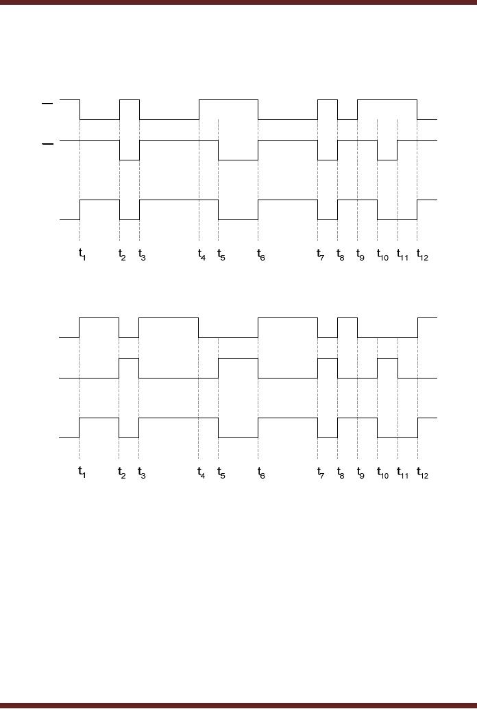
CS302 -
Digital Logic & Design
the
inputs S=0 and R=0
are not applied as it
results in an invalid output
state. Similarly, in
the
timing
diagram of the NOR based
S-R flip-flop, the inputs
S=1 and R=1 are
not applied as it
results in an
invalid output state.
S
R
Q
Figure
22.6a Timing diagram of an
active-low input S-R
latch
S
R
Q
Figure
22.6b Timing diagram of an
active-high input S-R
latch
223
Table of Contents:
- AN OVERVIEW & NUMBER SYSTEMS
- Binary to Decimal to Binary conversion, Binary Arithmetic, 1s & 2s complement
- Range of Numbers and Overflow, Floating-Point, Hexadecimal Numbers
- Octal Numbers, Octal to Binary Decimal to Octal Conversion
- LOGIC GATES: AND Gate, OR Gate, NOT Gate, NAND Gate
- AND OR NAND XOR XNOR Gate Implementation and Applications
- DC Supply Voltage, TTL Logic Levels, Noise Margin, Power Dissipation
- Boolean Addition, Multiplication, Commutative Law, Associative Law, Distributive Law, Demorgans Theorems
- Simplification of Boolean Expression, Standard POS form, Minterms and Maxterms
- KARNAUGH MAP, Mapping a non-standard SOP Expression
- Converting between POS and SOP using the K-map
- COMPARATOR: Quine-McCluskey Simplification Method
- ODD-PRIME NUMBER DETECTOR, Combinational Circuit Implementation
- IMPLEMENTATION OF AN ODD-PARITY GENERATOR CIRCUIT
- BCD ADDER: 2-digit BCD Adder, A 4-bit Adder Subtracter Unit
- 16-BIT ALU, MSI 4-bit Comparator, Decoders
- BCD to 7-Segment Decoder, Decimal-to-BCD Encoder
- 2-INPUT 4-BIT MULTIPLEXER, 8, 16-Input Multiplexer, Logic Function Generator
- Applications of Demultiplexer, PROM, PLA, PAL, GAL
- OLMC Combinational Mode, Tri-State Buffers, The GAL16V8, Introduction to ABEL
- OLMC for GAL16V8, Tri-state Buffer and OLMC output pin
- Implementation of Quad MUX, Latches and Flip-Flops
- APPLICATION OF S-R LATCH, Edge-Triggered D Flip-Flop, J-K Flip-flop
- Data Storage using D-flip-flop, Synchronizing Asynchronous inputs using D flip-flop
- Dual Positive-Edge triggered D flip-flop, J-K flip-flop, Master-Slave Flip-Flops
- THE 555 TIMER: Race Conditions, Asynchronous, Ripple Counters
- Down Counter with truncated sequence, 4-bit Synchronous Decade Counter
- Mod-n Synchronous Counter, Cascading Counters, Up-Down Counter
- Integrated Circuit Up Down Decade Counter Design and Applications
- DIGITAL CLOCK: Clocked Synchronous State Machines
- NEXT-STATE TABLE: Flip-flop Transition Table, Karnaugh Maps
- D FLIP-FLOP BASED IMPLEMENTATION
- Moore Machine State Diagram, Mealy Machine State Diagram, Karnaugh Maps
- SHIFT REGISTERS: Serial In/Shift Left,Right/Serial Out Operation
- APPLICATIONS OF SHIFT REGISTERS: Serial-to-Parallel Converter
- Elevator Control System: Elevator State Diagram, State Table, Input and Output Signals, Input Latches
- Traffic Signal Control System: Switching of Traffic Lights, Inputs and Outputs, State Machine
- Traffic Signal Control System: EQUATION DEFINITION
- Memory Organization, Capacity, Density, Signals and Basic Operations, Read, Write, Address, data Signals
- Memory Read, Write Cycle, Synchronous Burst SRAM, Dynamic RAM
- Burst, Distributed Refresh, Types of DRAMs, ROM Read-Only Memory, Mask ROM
- First In-First Out (FIFO) Memory
- LAST IN-FIRST OUT (LIFO) MEMORY
- THE LOGIC BLOCK: Analogue to Digital Conversion, Logic Element, Look-Up Table
- SUCCESSIVE APPROXIMATION ANALOGUE TO DIGITAL CONVERTER