 |
First In-First Out (FIFO) Memory |
| << Burst, Distributed Refresh, Types of DRAMs, ROM Read-Only Memory, Mask ROM |
| LAST IN-FIRST OUT (LIFO) MEMORY >> |
CS302 -
Digital Logic & Design
Lesson
No. 42
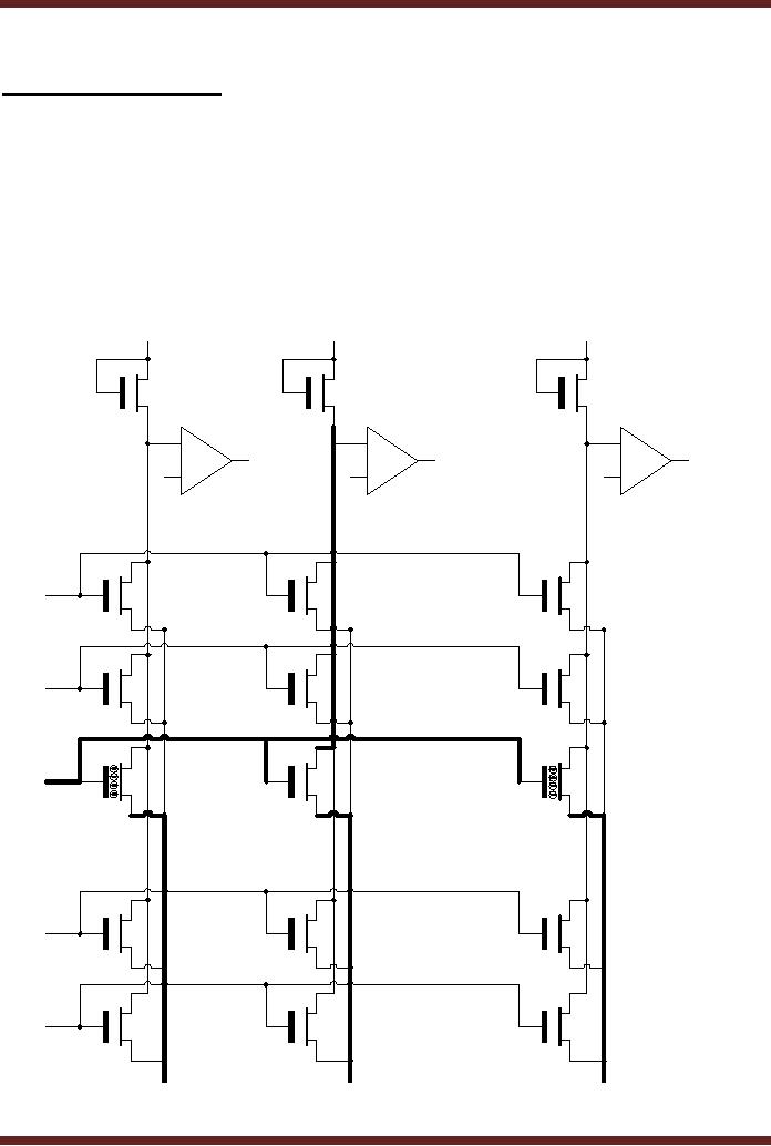
FLASH
MEMORY ARRAY
The
FLASH Memory array is
arranged in the form of rows
and columns. The row
line is
connected to
the Control Gate of each MOS
transistor which implements a
single bit storage
cell.
The number of such MOS
transistors in a row generally
depends upon the size of
the data
value
stored at each location. A
byte value stored at a
location requires 8 cells
activated by a
single
row. Only a single row is
selected at a time to select
the appropriate cells. The
Source
terminals of
all the transistors arranged
in a column are connected to a
column line.
Similarly,
the
transistors in the second
column have their Source
terminals connected
together.
Generally, if
the size of the data
stored is a byte, the memory
has eight column
lines
connecting
the Source of the
corresponding transistor cells in
each column together.
Figure
42.1.
+V
+V
+V
Active
Load
Active
Load
Active
Load
Comparator
Comparator
Comparator
Data
Data
Data
Out
0
Out
1
Out
7
Logic
1
Reference
Reference
Reference
Logic
1
Logic
0
Output
Output
Output
Row
Select
0
Row
Select
1
Row
Select
2
Stored
Stored
Stored
Logic
0
Logic
1
Logic
0
Row
Select
n-1
Row
Select
n
Column
Column
Column
Select
0
Select
1
Select
7
Figure
42.1
FLASH
Memory Array
423
CS302 -
Digital Logic & Design
When a
row is selected, (row 2 is
shown to be selected in the
figure) all the
transistors
which
have their Gate terminals
connected to the row select
line are activated. A
current flows
through
the selected transistor if
the corresponding column
select line is activated and
the
transistor
Gate has no charge stored.
In the figure, the column
select 0 line is
activated
however no
current flows through the
selected transistor as the
transistor gate has a
stored
charge.
The column select 1 line is
activated and a current
flows through the transistor
in the
second
column as the transistor
gate has no stored charge.
Similarly, no current flows
through
the
transistor in the last
column when the column
select 7 line is activated as
the transistor
gate
has a stored charge.
Thus no
current flows through a
column line if the selected
cells has a charge
stored
on the
transistor gate. If some of
the selected cells in a row
have charges stored while
others
do not
have charges stored then
current will not flow in
columns corresponding to the
cells
which
have charges stored, while
columns having current
flowing through them
correspond to
cells
having no charge. The
presence of current in a column
produces a voltage drop
across
an active
load connected at the end of
each column line, while an
absence of current
doesn't
produce a
voltage drop across the
active load. The voltage
drop produced across each
active
load is
separately compared with a
reference voltage by a comparator
circuit. If there is a
voltage
drop across the active
load due to flow of current,
the comparator output is a 0. If
the
voltage
drop across the active
load is 0 volts due to
absence of current the
comparator output
is a 1. The
presence or absence of current in a
column line is based on the
binary 1 and 0
stored in
the cell. Thus the
comparator output is opposite to
the information
stored.
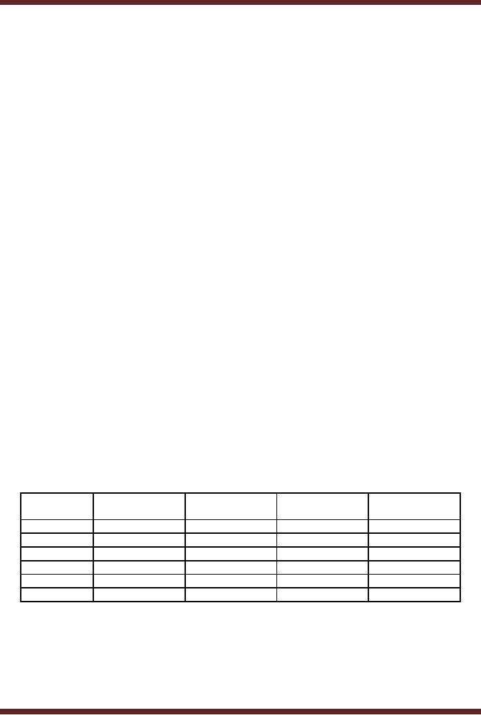
Memory
Summary
A summary of
memory types and their
characteristics are shown.
Table 42.1. The
Static
Ram (SRAM) is non-volatile
and is not a high density
memory as a latch is required
to
store a
single bit of information.
Implementation of a latch requires
almost six transistors.
The
Dynamic
Ram is also non-volatile
however it offers high
density memories as each
storage cell
requires a
single transistor and a
capacitor. ROMs and PROMs
retains information
permanently
even if the supply voltage
is removed. Since a single
transistor is used to store
a
logic 0 or 1
therefore ROMS and PROMs
are high density memories.
EEPROMs allow data to
be read or
written however the ability
to change the data without
having to remove the
EEPROM
chip from a circuit board
requires extra logic. Thus
EEPROM memories are not
high
density
memories.
Memory
Non-Volatile
High
Density
One-Transistor
In-System
Type
Cell
Write
ability
SRAM
No
No
No
Yes
DRAM
No
Yes
Yes
Yes
ROM
Yes
Yes
Yes
No
EPROM
Yes
Yes
Yes
No
EEPROM
Yes
No
No
Yes
FLASH
Yes
Yes
Yes
Yes
Table
42.1
A summary of
Memory Types
Special
Type of Memories
Two
types of memories namely the
first in-first out (FIFO)
memory and last in-first
out
(LIFO)
are implemented using shift
registers. These memories
are used in specific
applications.
424
CS302 -
Digital Logic & Design
First
In-First Out (FIFO)
Memory
Digital
systems receive data or
transfer data to devices
that are operating at
different
data
rates. A Computer (microprocessor),
for example, receives data
from the Keyboard as
a
user
types in the information.
The keyboard is a very slow
device which generates data
at a
rate of
few bytes per second.
The microprocessor on the
other hand is very fast
and can
processes
information at very high
data rates. Devices that
operate at different data
rates can
not be
connected to each other
directly through their data
lines because the devices
that
operate at
very high data rates
are slowed down to the
data rate of the slow
device. For
example, if a
microprocessor is connected directly to a
keyboard it would be waiting
for data
from
the keyboard. During the
waiting period the
microprocessor would not be
processing any
information
and would be lying idle.
Practically, a microprocessor is
connected to a keyboard
through a
keyboard buffer which is a
temporary memory where the
keyboard writes its
data
(the
keystrokes). The microprocessor
instead of waiting for the
keyboard is kept busy
processing
information. When ever the
microprocessor needs to use
the information typed
through
the keyboard it accesses the
keyboard buffer and reads
the necessary
information.
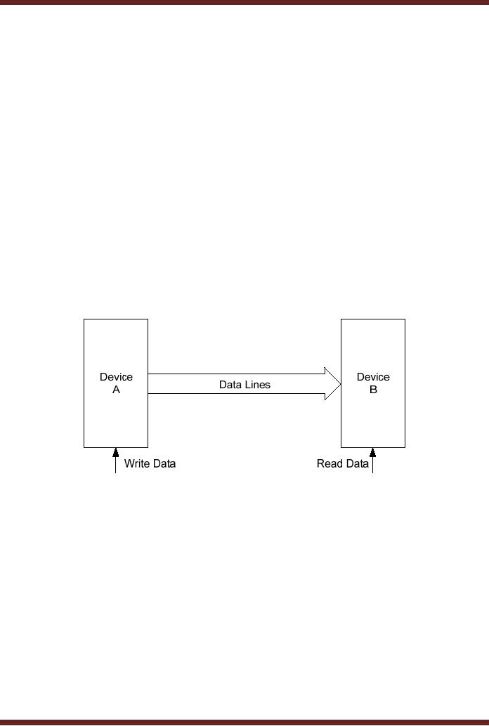
Two
devices operating at the
same data rates are
shown to be connected directly
through their
data
lines. Figure 42.2a. Since,
device A produces data at
the same rate at which
the device B
consumes
the data, the two
devices can be connected
together through their data
lines
without
the use of the buffer.
Device A is configured to write
data to the data lines
and device
B is configured
to read the data from
the data lines.
Figure
42.2a Devices A and B
operating at same data
rates
The
keyboard buffer is an example of a
FIFO memory. In the FIFO
scheme data is not
accessed
randomly from any location
as in RAM and ROM memories where
any location can
be accessed by
specifying the location
address. In the FIFO memory
the data which is
written
into
the memory first is the
first one to be read out. As
mentioned above, FIFO
memories are
used to
connect two digital devices
that produce and consume
data at different
rates.
Assuming
that Device A produces data
at a certain rate and device
B consumes the data at
a
different
rate. A FIFO memory is
connected between the output
of device A and the input
of
device B,
the data produced by device
A is written into the FIFO
memory. The device B
reads
the
data from the FIFO
memory in the same sequence
as was written by the device
A. Figure
42.2b.
425
CS302 -
Digital Logic & Design
Figure
42.2b FIFO Memory connecting
two communicating
devices
The
FIFO memory is implemented
using shift registers with a
control circuitry that
allow
the
data entered at the FIFO
input to be stored at the
FIFO output when the
FIFO memory is
empty.
Addition data that is
entered at the FIFO input is
shifted to the appropriate
location in
the
FIFO memory. When the
data at the FIFO output is
consumed by a device, the
stored data
within
the FIFO memory is shifted
forward so that the second
data to be input into the
FIFO
memory is
placed at the FIFO memory
output. Figure 42.2c.
Figure
42.2c Writing and Reading
from FIFO Buffer
In the
diagram data is produced by
the device in the sequence
7, 9, 1, 0 and 3. The
data is
written in the FIFO buffer
maintaining the sequence in
which the data values
are
produced.
Device B consumes the first
two values 7 and 9 leaving
the values 1, 0 and 3 in
the
buffer.
The data values in the
buffer are shifted towards
the head of the buffer to
create space
for
more data values to be
written. Device A produces
four new data values 5, 6, 1
and 2
which
are appended into the
buffer in the available
empty locations.
426
CS302 -
Digital Logic & Design
Figure
42.3
FIFO
Implementation using four
8-bit Shift Registers
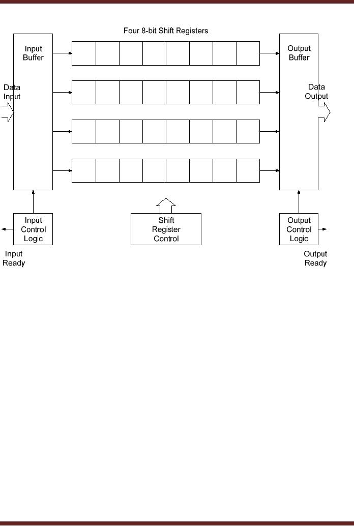
The
FIFO Implementation using
four, 8-bit shift registers
is shown. Figure 42.3.
Data
(4-bit
data) to be written into the
FIFO buffer is placed in the
Input Buffer which is
shifted to
appropriate
location by the Shift
Register Control circuit.
When the data is stored in
the FIFO
buffer at
the appropriate location the
Input Buffer is ready to
accept more data for
temporary
storage in
the FIFO buffer. The
Input Control Logic circuit
indicates the availability of
the Input
Buffer
for latching new data
values by activating the
Input Ready control signal.
The data is
read
out from the FIFO
buffer through the Output
Buffer. Data at the Buffer
Out location is
latched in by
the Output Buffer from
where the device can
read the data. Once
the data is read
the
Shift Control circuitry
updates the buffer by
shifting the buffer contents
towards the right.
The
right most data value in
the buffer is moved to the
Output Buffer latch for
reading by the
device.
The Output Ready signal is
activated to indicate the
availability of data for
reading.
Implementing
FIFO memory using
RAM
Shift
register based FIFO memory
is used in digital systems
designed for specific
applications
where small sized buffers
are used to allow transfer
of data between two
devices
operating at
different data rates. Such
digital systems either have
no RAM or very small RAM
for
storing variables. Computers
implement FIFO memory by
reserving a part of their
RAM
memory
for use as buffers. The
Keyboard buffer for example
is implemented by reserving a
part of
the RAM. When RAM is used as
FIFO memory, two registers
are used to point to
the
FIFO
Buffer Out and Buffer In
respectively. The two
registers hold the addresses
of the
locations of
the Buffer Out and
Buffer In respectively, which
are updated as new data is
written
into
the buffer and previous
data is read out from
the FIFO buffer.
Implementation of the
FIFO
buffer in RAM is
usually takes the form of a
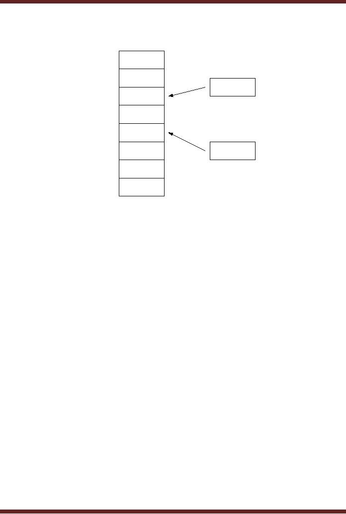
circular buffer. Figure
42.4.
427
CS302 -
Digital Logic & Design
Location
Buffer
Output
7
Address
Register
6
5
7
5
3
4
Buffer
Input
1
3
Address
Register
3
2
1
0
Figure
42.4
Implementation
of a FIFO buffer using
RAM
428
Table of Contents:
- AN OVERVIEW & NUMBER SYSTEMS
- Binary to Decimal to Binary conversion, Binary Arithmetic, 1s & 2s complement
- Range of Numbers and Overflow, Floating-Point, Hexadecimal Numbers
- Octal Numbers, Octal to Binary Decimal to Octal Conversion
- LOGIC GATES: AND Gate, OR Gate, NOT Gate, NAND Gate
- AND OR NAND XOR XNOR Gate Implementation and Applications
- DC Supply Voltage, TTL Logic Levels, Noise Margin, Power Dissipation
- Boolean Addition, Multiplication, Commutative Law, Associative Law, Distributive Law, Demorgans Theorems
- Simplification of Boolean Expression, Standard POS form, Minterms and Maxterms
- KARNAUGH MAP, Mapping a non-standard SOP Expression
- Converting between POS and SOP using the K-map
- COMPARATOR: Quine-McCluskey Simplification Method
- ODD-PRIME NUMBER DETECTOR, Combinational Circuit Implementation
- IMPLEMENTATION OF AN ODD-PARITY GENERATOR CIRCUIT
- BCD ADDER: 2-digit BCD Adder, A 4-bit Adder Subtracter Unit
- 16-BIT ALU, MSI 4-bit Comparator, Decoders
- BCD to 7-Segment Decoder, Decimal-to-BCD Encoder
- 2-INPUT 4-BIT MULTIPLEXER, 8, 16-Input Multiplexer, Logic Function Generator
- Applications of Demultiplexer, PROM, PLA, PAL, GAL
- OLMC Combinational Mode, Tri-State Buffers, The GAL16V8, Introduction to ABEL
- OLMC for GAL16V8, Tri-state Buffer and OLMC output pin
- Implementation of Quad MUX, Latches and Flip-Flops
- APPLICATION OF S-R LATCH, Edge-Triggered D Flip-Flop, J-K Flip-flop
- Data Storage using D-flip-flop, Synchronizing Asynchronous inputs using D flip-flop
- Dual Positive-Edge triggered D flip-flop, J-K flip-flop, Master-Slave Flip-Flops
- THE 555 TIMER: Race Conditions, Asynchronous, Ripple Counters
- Down Counter with truncated sequence, 4-bit Synchronous Decade Counter
- Mod-n Synchronous Counter, Cascading Counters, Up-Down Counter
- Integrated Circuit Up Down Decade Counter Design and Applications
- DIGITAL CLOCK: Clocked Synchronous State Machines
- NEXT-STATE TABLE: Flip-flop Transition Table, Karnaugh Maps
- D FLIP-FLOP BASED IMPLEMENTATION
- Moore Machine State Diagram, Mealy Machine State Diagram, Karnaugh Maps
- SHIFT REGISTERS: Serial In/Shift Left,Right/Serial Out Operation
- APPLICATIONS OF SHIFT REGISTERS: Serial-to-Parallel Converter
- Elevator Control System: Elevator State Diagram, State Table, Input and Output Signals, Input Latches
- Traffic Signal Control System: Switching of Traffic Lights, Inputs and Outputs, State Machine
- Traffic Signal Control System: EQUATION DEFINITION
- Memory Organization, Capacity, Density, Signals and Basic Operations, Read, Write, Address, data Signals
- Memory Read, Write Cycle, Synchronous Burst SRAM, Dynamic RAM
- Burst, Distributed Refresh, Types of DRAMs, ROM Read-Only Memory, Mask ROM
- First In-First Out (FIFO) Memory
- LAST IN-FIRST OUT (LIFO) MEMORY
- THE LOGIC BLOCK: Analogue to Digital Conversion, Logic Element, Look-Up Table
- SUCCESSIVE APPROXIMATION ANALOGUE TO DIGITAL CONVERTER