 |
CS302 -
Digital Logic & Design
Lesson
No. 25
ASYNCHRONOUS
PRESET AND CLEAR
INPUTS
The
S-R, J-K and D inputs
are known as synchronous
inputs because the
outputs
change
when appropriate input
values are applied at the
inputs and a clock signal is
applied at
the
clock input. If there is no
clock transition then the
inputs have no effect on the
output.
Digital
circuits require that the
flip-flops be set or reset to
some initial state before a
new set of
inputs is
applied for changing the
output. The flip-flops are
set-reset to some initial
state by
using
asynchronous inputs known as
Preset and Clear inputs.
Since these inputs change
the
output to a
known logic level
independently of the clock
signal therefore these
inputs are
known as
asynchronous inputs. The
circuit diagram of a J-K
flip-flop with Preset and
Set
Asynchronous
inputs is shown in figure
25.1a. The asynchronous
inputs override the
synchronous
inputs thus to operate the
flip-flop in the synchronous
mode the asynchronous
inputs
have to be disabled.
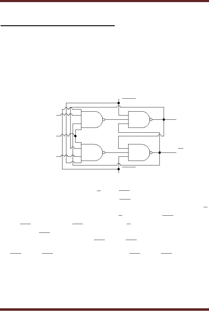
PRE
J
Q
3
1
CLK
Q
4
2
K
CLR
Figure
25.1a J-K flip-flop with
Asynchronous Preset and
Clear inputs
To preset
the flip-flop to Q=1 and
Q =0 the
PRE input is set to 0
which sets the Q
output to 1
and the output of NAND gate
4 to 1. The CLR input is set to 1, the
remaining two
inputs (Q
and output of NAND gate 4) of
the NAND gate 2 are also
set at logic 1, therefore Q
output is
set to 0. The flip-flop is
cleared to Q=0 and Q =1 by setting
the PRE input is set to 1
and
the CLR input is to 0. The CLR input set to 0
sets Q =1 it also
sets the output of
NAND
gate 3 to 1.
The PRE input along with
the other two inputs of NAND
gate 1 are set at logic
1
which
sets the output Q to 0. When
the PRE and the CLR inputs are
used inputs J and K
have no
effect on the operation of
the flip-flop. To use the
flip-flop with synchronous
inputs J-K,
the PRE and the CLR inputs are
set to logic 1. Setting PRE and the CLR to logic 0 is
not
allowed.
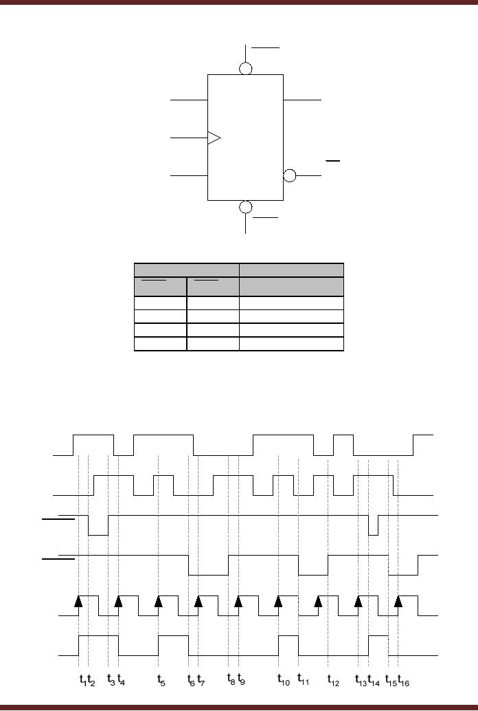
Logic
symbol of a J-K edge-triggered
flip-flop with synchronous
and asynchronous
inputs is
shown in figure 25.1b. The
truth table of a J-K
flip-flop with Asynchronous
inputs is
shown in
table 25.1. The timing
diagram describes the effect
of asynchronous inputs on
the
operation of
the flip-flop. Figure
25.1c
255
CS302 -
Digital Logic & Design
PRE
J
Q
J-K
CLK
Flip-Flop
K
Q
CLR
Figure
25.1b Logic Symbol of a J-K
flip-flop with Asynchronous
inputs
Input
Output
Qt+1
CLR
PRE
0
0
Invalid
0
1
1
1
0
0
1
1
Clocked
operation
Table
25.1
Truth
table of J-K flip-flop with
Asynchronous inputs
J
K
PRE
CLR
CLK
Q
Figure
25.1c Timing diagram of a
J-K flip-flop with Preset
and Clear inputs
256

CS302 -
Digital Logic & Design
The
74HC74 Dual Positive-Edge
triggered D flip-flop
The
edge-triggered D flip-flop with
asynchronous inputs is available as an
Integrated
Circuit.
The 74HC74 has dual
D-flip-flops with independent
clock inputs, synchronous
and
asynchronous
inputs.
The
74HC112 Dual Positive-Edge
triggered J-K
flip-flop
The
edge-triggered D flip-flop with
asynchronous inputs is available as an
Integrated
Circuit.
The 74HC112 has dual
J-K-flip-flops with independent
clock inputs, synchronous
and
asynchronous
inputs.
Master-Slave
Flip-Flops
Master-Slave
flip-flops have become
obsolete and are replaced by
edge-triggered flip-
flops.
Master-Slave flips have two
stages each stage works in
one half of the clock
signal. The
inputs
are applied in the first
half of the clock signal.
The outputs do not change
until the
second
half of the clock signal. As
mentioned earlier the use of
edge-triggered flip-flip is to
synchronize
the operation of a digital
circuit with a common clock
signal. The
master-slave
setup
also allows digital circuits
to operate in synchronization with a
common clock signal.
The
circuit
diagram of the master-slave
J-K flip-flop is shown in
figure 25.2a. The
Master-Slave flip-
flop is
composed of two parts the
Master and the Slave.
Both the Master and
the Slave are
Gated
S-R flip-flops. The
Master-Slave flip-flop is not
synchronised with the clock
positive or
negative
transition, rather it known as a
pulse triggered flip-flop as it
operates at the
positive
and
negative clock
cycles.
Consider
that the J-K inputs of
the flip-flop are set at 1
and 0 respectively. The
outputs
Q and
Q are
initially set at 1 and 0
respectively. During the
positive half of the clock
gates 3
and 4
are both enabled by the
clock signal. The output of
gate 3 is set to 1 due to
the Q
output
set at 0. Similarly the
output of gate 4 is also set
at 1 due to the K input set
at 0. The
outputs of
gates 1 and 2 remain
unchanged as the inputs to
gates 1 and 2 are both
logic 1.
Assume
the outputs of gates 1 and 2
to be 1 and 0 respectively. During
the positive half
cycle,
the
clock input to gates 7 and 8
is inverted therefore both
the gates are disabled
and their
output is
set to logic 1. With logic 1
at the inputs of gates 5 and
6 the output Q and Q remains
unchanged
throughout the positive half
of the clock cycle. During
the negative half of the
clock
cycle
the Master flip-flop is
disabled and the output of
the Master flip-flop remains
fixed during
the
negative half cycle. The
Slave flip-flop is enabled
and the 1 and 0 outputs of
the Master
flip-flop
set the Q and Q output to 1
and 0 respectively.
Initially, if
the Q and Q outputs
are 0 and 1 respectively,
setting the J and K inputs
to 1
and 0
respectively sets the output
to 1 and 0 respectively. During
the positive half of the
clock
the
Master flip-flop is enabled,
the output of gate 3 is set
to 0 as the J, Q and CLK
inputs are
all at
logic 1. The output of gate
4 is set to 1 as the K input is
logic 0. These inputs set
the
output of
the Master flip-flop at
gates 1 and 2 to logic 1 and
0 respectively. During the
negative
half of
the clock cycle the
Slave flip-flop is enabled
the output Q and Q are
set to logic 1 and 0
respectively.
257
CS302 -
Digital Logic & Design
J
Q
3
1
7
5
CLK
Q
4
2
8
6
K
MASTER
SLAVE
Figure
25.2a Master-Slave
flip-flop
The
truth-table of the master-slave
flip-flop is shown in table
25.2. The timing
diagram
of the
master-slave flip-flop is shown in
figure 25.2b.
Input
Output
CLK
J
K
Qt+1
Pulse
0
0
Qt
Pulse
0
1
0
Pulse
1
0
1
Pulse
1
1
Qt
Table
25.2
Truth
table of the Master-Slave
J-K flip-flop
J
K
CLK
Q
Figure
25.2b Timing diagram of a
Master Slave J-K
flip-flop
Flip-Flop
Operating Characteristics
The
performance of the flip-flop is
specified by several operating
characteristics
mentioned in
the data sheets of the
flip-flops. The important
operating characteristics
are
258
CS302 -
Digital Logic & Design
·
Propagation
Delay
·
Set-up
Time
·
Hold
Time
·
Maximum
Clock frequency
·
Pulse
width
·
Power
Dissipation
Propagation
Delay
The
propagation delay time is
the interval of time when
the input is applied and
the
output
changes. Four different
types of Propagation Delays
are measured.
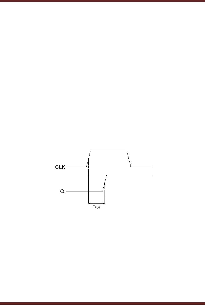
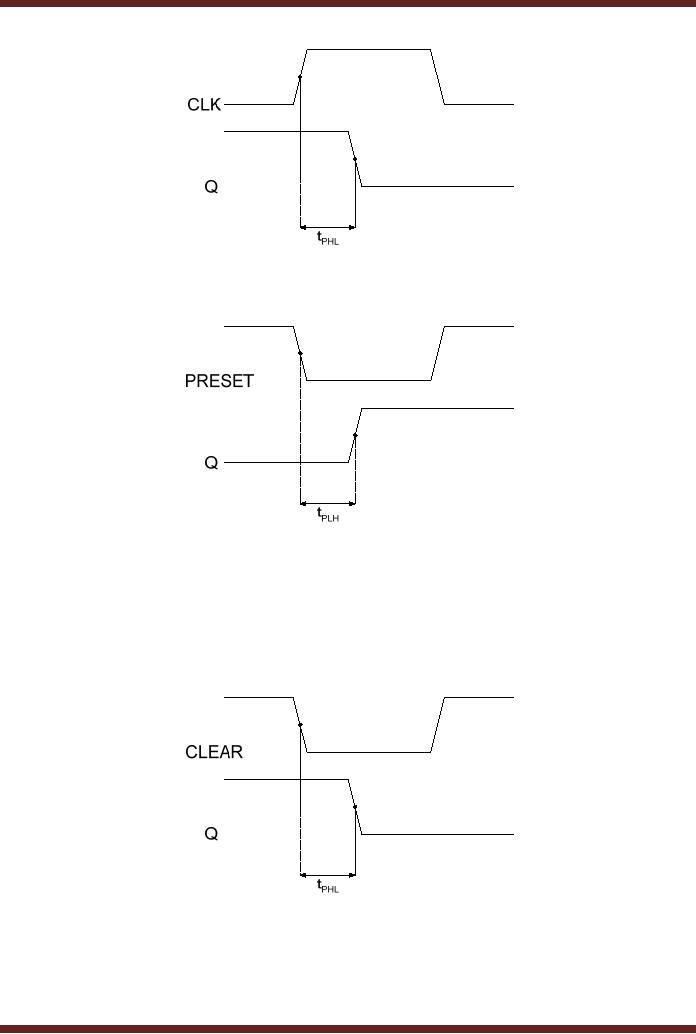
5. Propagtaion
Delay tPLH measured with respect to
the triggering edge of the
clock to the
low-to-high
transition of the output.
Figure 25.3. On a positive or
negative clock
transition
the
flip-flop changes its output
state. The Propagation Delay
is measured at 50%
transition
mark on
the triggering edge of the
clock and the 50%
mark on the low-to-high
transition of
the
output that occurs due to
the clock transition.
6. Propagtaion
Delay tPHL measured with respect to
the triggering edge of the
clock to the
high-to-low
transition of the output.
Figure 25.4. On a positive or
negative clock
transition
the
flip-flop changes its output
state. The Propagation Delay
is measured at 50%
transition
mark on
the triggering edge of the
clock and the 50%
mark on the high-to-low
transition of
the
output that occurs due to
the clock transition.
Figure
25.3
Propagation
Delay, clock to low-to-high
transition of the
output
7. Propagtaion
Delay tPLH measured with respect to
the leading edge of the
preset input to the
low-to-high
transition of the output.
Figure 25.5. On a high-to-low
transition of the
preset
signal
the flip-flop changes its
output state to logic high.
The Propagation Delay
is
measured at
50% transition mark on the
triggering edge of the
preset signal and the
50%
mark on
the low-to-high transition of
the output that occurs
due to the preset
signal.
259
CS302 -
Digital Logic & Design
Figure
25.4
Propagation
Delay, clock to high-to-low
transition of the
output
Figure
25.5
Propagation
Delay, preset to low-to-high
transition of the
output
8. Propagtaion
Delay tPHL measured with respect to
the leading edge of the
clear input to the
high-to-low
transition of the output.
Figure 25.6. On a high-to-low
transition of the
clear
signal
the flip-flop changes its
output state to logic low.
The Propagation Delay
is
measured at
50% transition mark on the
triggering edge of the clear
signal and the
50%
mark on
the high-to-low transition of
the output that occurs
due to the preset
signal.
Figure
25.6
Propagation
Delay, clear to high-to-low
transition of the
output
Set-up
Time
When a
clock transition occurs at
the clock input of a
flip-flop the output of the
flip-flop
is set to a
new state based on the
inputs. For the flip-flop to
change its output to a new
state at
the
clock transition, the input
should be stable. The
minimum time required for
the input logic
260
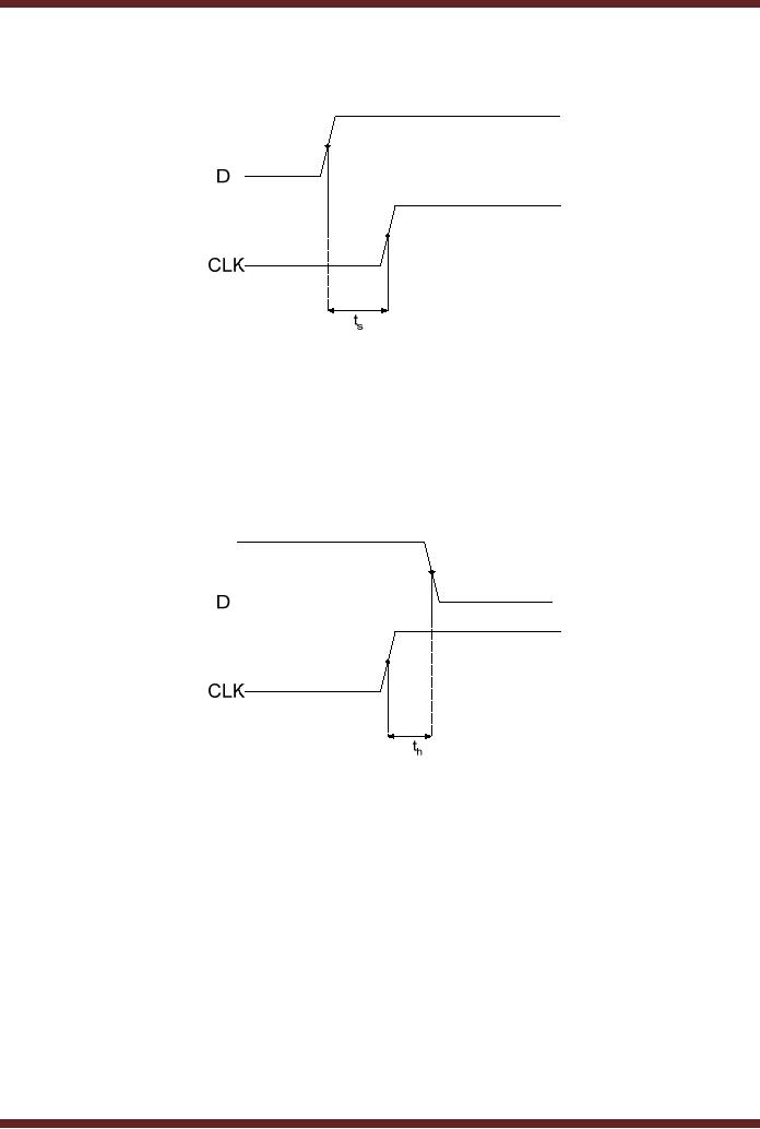
CS302 -
Digital Logic & Design
levels to
remain stable before the
clock transition occurs is
known as the Set-up time.
Figure
25.7
Figure
25.7
Set-up
time for a D
flip-flop
Hold
Time
The
input signal maintained at
the flip-flop input has to
be maintained for a
minimum
time
after the clock transition
for the flip-flop to
reliably clock in the input
signal. The minimum
time
for which the input
signal has to be maintained at
the input is the Hold
time of the
flip-flop.
Figure
25.8
Figure
25.8
Hold
time for a D
flip-flop
Maximum
Clock Frequency
A flip-flop
can be operated at a certain
clock frequency. If the
clock frequency is
increased
beyond a certain limit the
flip-flop will be unable to
respond to the fast
changing
clock
transitions, therefore the
flip-flop will be unable to
function. The maximum
clock
frequency
fmax is the highest
rate at which the flip-flop
operates reliably.
Pulse
Width
A flip-flop
uses the clock, preset
and clear inputs for
its operation. Each signal
has to
be of a
specified duration for
correct operation of the
flip-flop. The manufacturer
specifies the
minimum
pulse width tw for
each of the three signals.
The clock signal is
specified by minimum
high
time and minimum low
time.
261
CS302 -
Digital Logic & Design
Power
Dissipation
A flip-flop
consumes power during its
operation. The power
consumed by a flip-flop is
defined by P =
Vcc x Icc. The
flip-flop is connected to +5 volts
and it draws 5 mA of
current
during
its operation, therefore the
power dissipation of the
flip-flop is 25 mW.
A digital
circuit is made of a number of
gates, functional units and
flip-flops. The total
power
requirement of each device
should be known so that an
appropriate dc power source
is
used to
supply power to the digital
circuit.
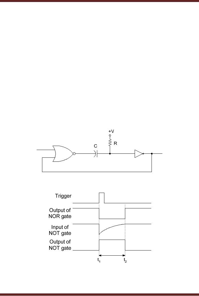
One-Shot
Mono-stable multi-vibrator
Bi-stable
devices remain in either of
their two states unless
the inputs force the
device
to switch
its state. The device
remains in its alternate
state unless the inputs
are changed
again to
force the device back to
its original state. A
mono-stable device only has
a single
stable
state and it remains in its
stable state. It temporarily
changes to its unstable
state when
it is triggered.
It remains in its unstable
state for a predetermined
length of time and then
it
automatically
switches back to its stable
state. The length of time
for which the device
remains
in the
unstable state is determined by
the time constant determined
by the Resistor and
Capacitor
connected externally to the
mon-stable device. The
output of the device is a
pulse
having a
time duration determined by R
and C. These mono-stable
devices are also known
as
One-Shots.
Figure 25.9. One-Shots are
of two types, the
nonretriggerable and
retriggerable.
Figure
25.9a Circuit diagram of a
One-Shot
Figure
25.9b Timing diagram of a
One-Shot
The
One-Shot is triggered by applying a
short pulse at the input of
the NOR gate at
time
interval t1. The
One-Shot is in its stable
state with output at logic
zero at time interval < t1.
The
logic high triggering pulse
at the input of the NOR
gate sets its output to
logic low. The
262
CS302 -
Digital Logic & Design
logic
low output of the NOR
gate is inverted into logic
high by the NOT gate
and the One-Shot
is in unstable
state at the start of
interval t1. The
logic high output of the
NOT gate is
connected
back to the second input of
the NOR gate, which
maintains the output of the
NOR
gate at
logic low. When the
output of the NOR gate is
set to logic low at interval
t1, the
capacitor C
begins charging through the
Resistor R. The charging
time (in seconds) is
determined by
the time constant RC.
During the charging of the
capacitor during interval t1 to
t2, the input of the
NOT gate remains at logic
low, therefore the output of
the NOT gate
remains in
the unstable state at logic
high. When the capacitor is
fully charged to potential
+V
(logic
high) at time interval t2, the NOT gate
input also become logic
high, which sets
the
output of
the NOT gate to logic
low. With the setting of
the NOT gate output to
logic low at
interval
t2, the One-Shot id
switched back to its stable
state. The interval t1 to t2 during
which
the
One-Shot is in its unstable
state is determined by the
time constant RC.
1.
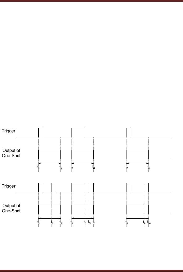
Nonretriggerable One-Shot
A
nonretriggerable OneShot is
triggered to its unstable
state.
a. The
One-Shot output remains in
the unstable state for a
fixed period of time on
each
trigger
input.
b. The
One-Shot will have to return
to its stable state before
it can be triggered again. If it
is
already in
its unstable state due to
application of a trigger input, a
new trigger input
will
have no
effect.
c. The
duration of trigger input
pulses has no effect on the
output pulse duration. The
One-
Shot is
triggered either on the
positive or the negative
edge. Figure 25.10
Figure
25.10a Timing diagram of a
non-retriggerable One-Shot
Figure
25.10b Timing diagram of a
non-retriggerable One-Shot with
ignored triggers
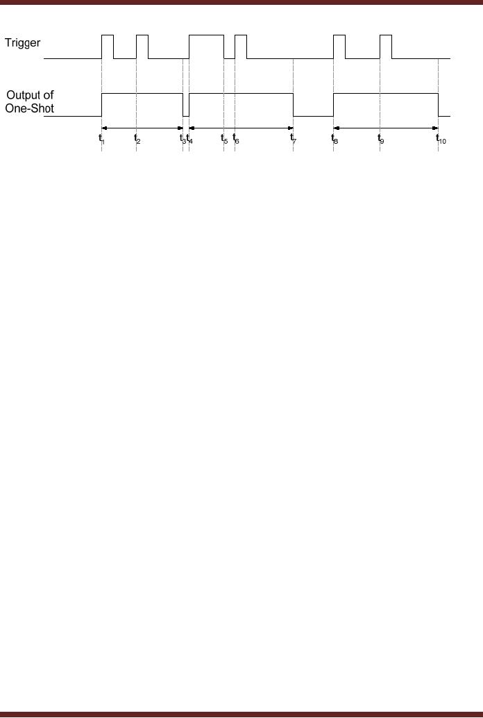
2. Retriggerable
One-Shot
A retriggerabe
One-Shot operation is very
similar to that of the
Nonretriggerbale One-Shot
except
that the retriggerable
One-Shot will retrigger even
if it is in its unstable state.
Figure
25.11.
The retriggerable and
Nonretriggerbale are available in
Integrated Circuit
form.
263
CS302 -
Digital Logic & Design
Figure
25.11 Timing diagram of a
Retriggerable One-Shot
264
Table of Contents:
- AN OVERVIEW & NUMBER SYSTEMS
- Binary to Decimal to Binary conversion, Binary Arithmetic, 1s & 2s complement
- Range of Numbers and Overflow, Floating-Point, Hexadecimal Numbers
- Octal Numbers, Octal to Binary Decimal to Octal Conversion
- LOGIC GATES: AND Gate, OR Gate, NOT Gate, NAND Gate
- AND OR NAND XOR XNOR Gate Implementation and Applications
- DC Supply Voltage, TTL Logic Levels, Noise Margin, Power Dissipation
- Boolean Addition, Multiplication, Commutative Law, Associative Law, Distributive Law, Demorgans Theorems
- Simplification of Boolean Expression, Standard POS form, Minterms and Maxterms
- KARNAUGH MAP, Mapping a non-standard SOP Expression
- Converting between POS and SOP using the K-map
- COMPARATOR: Quine-McCluskey Simplification Method
- ODD-PRIME NUMBER DETECTOR, Combinational Circuit Implementation
- IMPLEMENTATION OF AN ODD-PARITY GENERATOR CIRCUIT
- BCD ADDER: 2-digit BCD Adder, A 4-bit Adder Subtracter Unit
- 16-BIT ALU, MSI 4-bit Comparator, Decoders
- BCD to 7-Segment Decoder, Decimal-to-BCD Encoder
- 2-INPUT 4-BIT MULTIPLEXER, 8, 16-Input Multiplexer, Logic Function Generator
- Applications of Demultiplexer, PROM, PLA, PAL, GAL
- OLMC Combinational Mode, Tri-State Buffers, The GAL16V8, Introduction to ABEL
- OLMC for GAL16V8, Tri-state Buffer and OLMC output pin
- Implementation of Quad MUX, Latches and Flip-Flops
- APPLICATION OF S-R LATCH, Edge-Triggered D Flip-Flop, J-K Flip-flop
- Data Storage using D-flip-flop, Synchronizing Asynchronous inputs using D flip-flop
- Dual Positive-Edge triggered D flip-flop, J-K flip-flop, Master-Slave Flip-Flops
- THE 555 TIMER: Race Conditions, Asynchronous, Ripple Counters
- Down Counter with truncated sequence, 4-bit Synchronous Decade Counter
- Mod-n Synchronous Counter, Cascading Counters, Up-Down Counter
- Integrated Circuit Up Down Decade Counter Design and Applications
- DIGITAL CLOCK: Clocked Synchronous State Machines
- NEXT-STATE TABLE: Flip-flop Transition Table, Karnaugh Maps
- D FLIP-FLOP BASED IMPLEMENTATION
- Moore Machine State Diagram, Mealy Machine State Diagram, Karnaugh Maps
- SHIFT REGISTERS: Serial In/Shift Left,Right/Serial Out Operation
- APPLICATIONS OF SHIFT REGISTERS: Serial-to-Parallel Converter
- Elevator Control System: Elevator State Diagram, State Table, Input and Output Signals, Input Latches
- Traffic Signal Control System: Switching of Traffic Lights, Inputs and Outputs, State Machine
- Traffic Signal Control System: EQUATION DEFINITION
- Memory Organization, Capacity, Density, Signals and Basic Operations, Read, Write, Address, data Signals
- Memory Read, Write Cycle, Synchronous Burst SRAM, Dynamic RAM
- Burst, Distributed Refresh, Types of DRAMs, ROM Read-Only Memory, Mask ROM
- First In-First Out (FIFO) Memory
- LAST IN-FIRST OUT (LIFO) MEMORY
- THE LOGIC BLOCK: Analogue to Digital Conversion, Logic Element, Look-Up Table
- SUCCESSIVE APPROXIMATION ANALOGUE TO DIGITAL CONVERTER