 |
CS302 -
Digital Logic & Design
Lesson
No. 27
DOWN
COUNTERS
All
the examples considered so
far have used counters
that count up from binary
zero
to some
maximum count value
depending upon the Modulus
value of the counter. When
the
counter
reaches its maximum count
value it is reset to binary
zero and continues with
the
counting
sequence. A down counter
counts in a sequence which
starts with some
maximum
count
value and counts down to
binary zero. It is then
reset to the maximum count
value and
repeats
the counting sequence. A
Down-counter is implemented by connecting
the Q output
instead of
the Q output of all the
flip-flops to the clock
inputs of the next
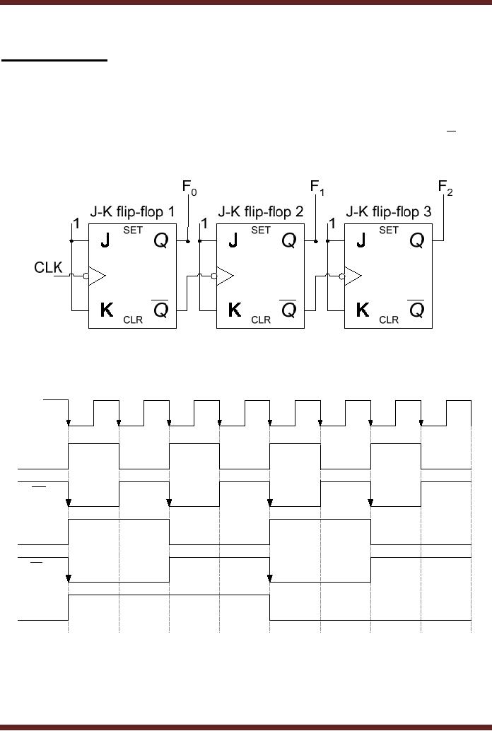
flip-flops. Figure
27.1
Figure
27.1a 3-bit Asynchronous
Down-Counter
CLOCK
Input
F0
F0
F1
F1
F2
t9
t2
t3
t4
t5
t6
t7
t8
t1
Figure
27.1b Timing diagram of a
3-bit Asynchronous
Down-Counter
277
CS302 -
Digital Logic & Design
Down
Counter with truncated
sequence
A down
counter can be configured to
count down a truncated
sequence, similar to an
up-counter
which can count up to any
truncated sequence. A down
counter counts down
from
the
maximum count value to some
predefined count value which
is the last count value in
the
truncated
sequence. On reaching the
last count value the
down-counter is preset to
the
maximum
count value instead of
clearing the counter to zero
count value as done in the
case
of an
up-counter. The circuit
shows a 3-bit down-counter
configured to count down a
truncated
sequence
from 111 to 011. On reaching
the count value 011,
the counter is preset to
111
when it is
decremented to 010 on the
negative clock transition.
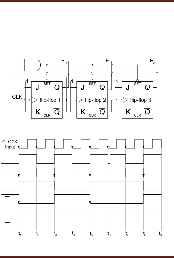
Figure 27.2
Figure
27.2a Down-counter configured to
count a truncated
sequence
F0
F0
F1
F1
F2
F2
Figure
27.2b Timing diagram of a
counter configured to count a
truncated sequence
278
CS302 -
Digital Logic & Design
The
counter counts down from
111 to 011 from interval
t1 to interval t5. At interval t6 the
counter
counts down to 010, the
F0 , F1
and F2
are
set to logic 1, the output
of the NAND gate
is set to
logic 0 which presets all
the three flip-flops to
state 111. The counter
continues with its
counting
sequence and at the clock
transition at interval t7 and t8
the
counter count down to
110
and 101 respectively.
Synchronous
Counters
Asynchronous
counters due to the delayed
outputs caused by the
rippling clock signal
do not
allow their operation with
high frequency clock
signals. Asynchronous counters
having
multiple
bits also cause timing
problems due to the
excessive propagation
delays.
Applications
requiring 8, 16 and 32 counters
and operating at high clock
frequencies
are
implemented using Synchronous
Counters. Synchronous counters
use a common clock
signal
connected to the clock
inputs of all the counter
flip-flops. Therefore, on a clock
transition
all
the flip-flops simultaneously
change their output state.
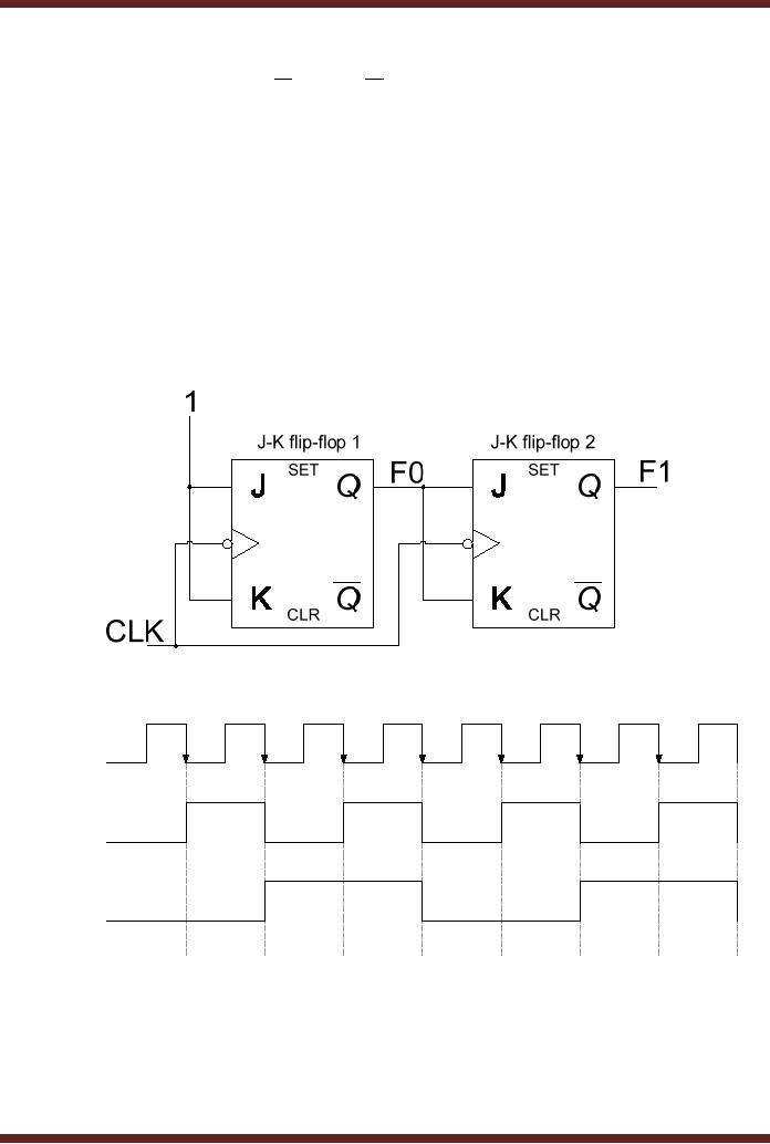
Figure 27.3.
Figure
27.3a 2-bit Synchronous
Counter
CLOCK
Input
F0
Output
F1
Output
t1
t2
t3
t4
t5
t6
t7
t8
Figure
27.3b Timing diagram of a
2-bit Synchronous
Counter
The
2-bit Synchronous counter
has both its clock
inputs connected to the
clock signal.
Both
the flip-flops are reset to
logic low states
respectively. On a high to low
clock transition at
interval
t1, the F0 output of the first
flip-flop toggles to logic
high. Since the clock
transition on
279
CS302 -
Digital Logic & Design
the
clock input of the second
flip-flop also occurs at
interval t1, the
J-K inputs of the second
flip-
flop
are at interval t1 are at
logic 0. The change at the
inputs J-K to logic 1 of the
second flip-
flop
occurs after a propagation
delay tPLH of
the first flip-flop. Thus
the output of the second
flip-
flop
remains unchanged due to the
input condition at the J-K
inputs (J=0, K=0). At
interval t2
the
output F0
is at logic
high (1) along with
the J-K inputs as the
three are connected
together.
On a clock
transition at interval t2 the output F0 toggles to logic 0. At the
very same instant
the
output
F1 also toggles to
logic 1. The inputs J-K of
the second flip-flop is set
to logic 0 after a
propagation
delay of tPHL of
the first flip-flop. At
interval t3, at
the clock transition the
output F0
toggles to
logic 1. The inputs J-K of
the second flip-flop at time
interval t3
is logic 0
therefore at
the
clock transition the output
F1 remains unchanged.
The inputs J-K of the
second flip-flop
change
after a propagation delay of
tPLH. Finally, at time
interval t4, the
output F0
of the
first flip-
flop
toggles to logic 0. The J-K
inputs of the second
flip-flop are at logic 1,
therefore the output
F1 of the second flip-flop is
also set to logic 0.
3-bit &
4-bit Synchronous
Counters
Multi-bit
Synchronous Counters can
easily be implemented by connecting
together
appropriate
number of flip-flops together.
The clock inputs of all
the flip-flops are
directly
connected to a
common clock signal.
Implementing of Synchronous Counters
larger than 2-
bits
requires the use of an AND
gate. Figure 27.4
F0
F1
F2
1
SET
SET
SET
Q
Q
Q
flip-flop
1
flip-flop
2
flip-flop
3
Q
Q
Q
CLR
CLR
CLR
CLK
Figure
27.4a
A 3-bit
Synchronous Counter
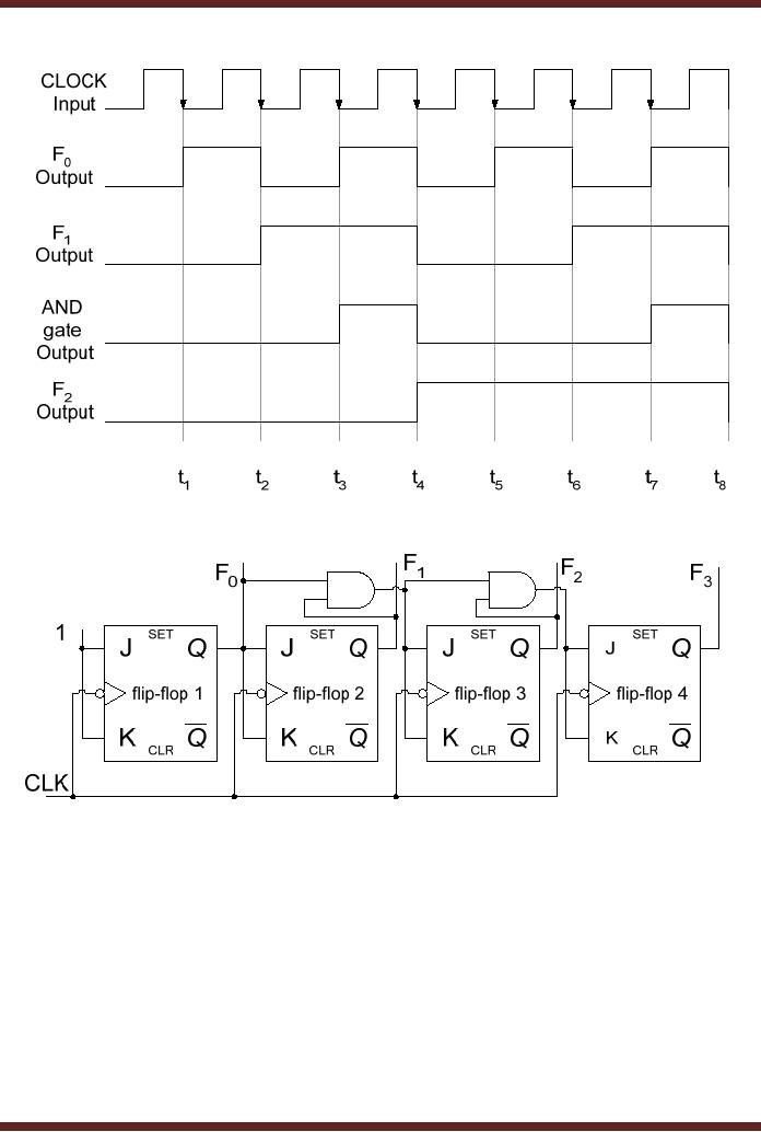
The
operation of the 3-bit
Synchronous Counter and the
need for the AND gate
can be
understood by
studying the timing diagram
of the 3-bit counter. The
timing of the first two
flip-
flops is
identical to the timings of
the 2-bit counter discussed
earlier. The timing
diagram
shows
that at interval t4,
the 3-bit counter should
count from state 011 to
100. Similarly, at
interval
t8 the counter
should count from state
111 to 000. At both the
intervals the F2 output of
the
third flip-flop toggles to
logic 1 and logic 0
respectively when the
outputs F0
and F1 are both
at logic 1.
This is implemented by connecting
the two outputs F0 and F1
to the
inputs of a 2-
input AND
gate. The output of the AND
gate is logic 1 when both
its inputs (F0 and
F1) are at
logic 1.
The output of the AND gate
is connect to the J-K inputs
of the third flip-flop. If
the AND
gate is
not used and the
J-K inputs of the third
flip-flop are directly
connected to the output F1
of the
second flip-flop, the third
flip-flop will change its
state and set its
output F2
to logic 1
at
the
time interval t3.
The count sequence is thus
disturbed.
280
CS302 -
Digital Logic & Design
Figure
27.4b
Timing
diagram of a 3-bit Synchronous
Counter
Figure
27.5
4-bit
Synchronous Binary
Counter
Larger
counters can be implemented
using similar AND gates. For
example, a 4-bit
counter
uses four flip-flops. The
counter circuit for the
first three flip-flops is
identical to the 3-
bit
counter circuit. The input
of the fourth flip-flop is
connected through a 3-input AND
gate with
inputs
F0, F1 and
F2. The fourth
flip-flop changes its state
when the outputs of the
first three
flip-flops
are at logic 1. That is,
the when the 4-bit
counter is counting from
0111 to 1000 and
1111 to
0000. Figure 27.5
4-bit
Synchronous Decade
Counter
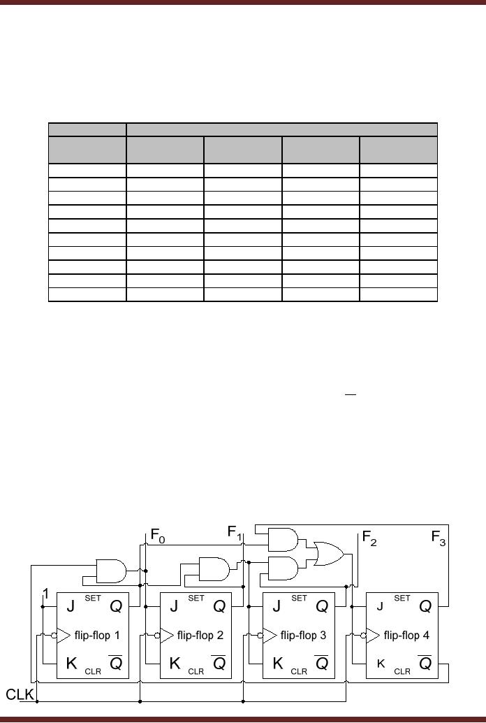
Earlier, an
Asynchronous Decade counter
has been discussed, which
counts from
state
0000 to 1001. The
Asynchronous counter is cleared to
state 0000 when the
counter
counts
from 1001 to 1010.
Synchronous counter can be
implemented which counts
from 0000
to 1001. In
the synchronous counter, all
the four flip-flops are
connected to a common
clock
281
CS302 -
Digital Logic & Design
and
are triggered simultaneously.
However, instead of using
the clear asynchronous
inputs to
clear
the counter to the initial
state, logic gates are
used to reset the decade
counter to state
0000
after it reaches state 1001.
The implementation of the
Synchronous Decade counter
can
be understood
with the help of a function
table that represents the
operation of the
Decade
Counter.
Table 27.1.
Input
Output
Clock
F3
F2
F1
F0
Pulses
1
0
0
0
0
2
0
0
0
1
3
0
0
1
0
4
0
0
1
1
5
0
1
0
0
6
0
1
0
1
7
0
1
1
0
8
0
1
1
1
9
1
0
0
0
10
1
0
0
1
Table
27.1
Output of a
Synchronous Decade
Counter
The
output state of the first
flip-flop F0
is shown to
toggle between 1 and 0 on
each
clock
transition. Therefore, the
inputs J-K of the first
flip-flop are connected to
logic high. The
output
state of the second
flip-flop F1
changes
from logic 0 to logic 1 and
vice- verse when F0
output is
logic 1 and F3 output is logic 0.
Therefore, the inputs J-K of
the second flip-flop
are
connected to a
function determined by the
Boolean expression F0 F3 . The
output state of the
third
flip-flop F2
changes
from logic 0 to logic 1 and
vice-versa when F0 and
F1 outputs are
both
at logic 1.
Therefore, the inputs J-K of
the third flip-flop are
connected to a function
determined
by the
Boolean expression F0F1 . The
output of the fourth
flip-flop F3
changes
its output state
when
outputs F0, F1 and F2
are at
logic 1 or when outputs F0 and F3
are at
logic 1. Therefore,
the
J-K inputs of the fourth
flip-flop are connected to a
function determined by a
Boolean
expression
F0F1F2 + F0F3 . The
decade counter is shown in
figure 27.6
282

CS302 -
Digital Logic & Design
Figure
27.6
Synchronous
Decade Counter
283
Table of Contents:
- AN OVERVIEW & NUMBER SYSTEMS
- Binary to Decimal to Binary conversion, Binary Arithmetic, 1s & 2s complement
- Range of Numbers and Overflow, Floating-Point, Hexadecimal Numbers
- Octal Numbers, Octal to Binary Decimal to Octal Conversion
- LOGIC GATES: AND Gate, OR Gate, NOT Gate, NAND Gate
- AND OR NAND XOR XNOR Gate Implementation and Applications
- DC Supply Voltage, TTL Logic Levels, Noise Margin, Power Dissipation
- Boolean Addition, Multiplication, Commutative Law, Associative Law, Distributive Law, Demorgans Theorems
- Simplification of Boolean Expression, Standard POS form, Minterms and Maxterms
- KARNAUGH MAP, Mapping a non-standard SOP Expression
- Converting between POS and SOP using the K-map
- COMPARATOR: Quine-McCluskey Simplification Method
- ODD-PRIME NUMBER DETECTOR, Combinational Circuit Implementation
- IMPLEMENTATION OF AN ODD-PARITY GENERATOR CIRCUIT
- BCD ADDER: 2-digit BCD Adder, A 4-bit Adder Subtracter Unit
- 16-BIT ALU, MSI 4-bit Comparator, Decoders
- BCD to 7-Segment Decoder, Decimal-to-BCD Encoder
- 2-INPUT 4-BIT MULTIPLEXER, 8, 16-Input Multiplexer, Logic Function Generator
- Applications of Demultiplexer, PROM, PLA, PAL, GAL
- OLMC Combinational Mode, Tri-State Buffers, The GAL16V8, Introduction to ABEL
- OLMC for GAL16V8, Tri-state Buffer and OLMC output pin
- Implementation of Quad MUX, Latches and Flip-Flops
- APPLICATION OF S-R LATCH, Edge-Triggered D Flip-Flop, J-K Flip-flop
- Data Storage using D-flip-flop, Synchronizing Asynchronous inputs using D flip-flop
- Dual Positive-Edge triggered D flip-flop, J-K flip-flop, Master-Slave Flip-Flops
- THE 555 TIMER: Race Conditions, Asynchronous, Ripple Counters
- Down Counter with truncated sequence, 4-bit Synchronous Decade Counter
- Mod-n Synchronous Counter, Cascading Counters, Up-Down Counter
- Integrated Circuit Up Down Decade Counter Design and Applications
- DIGITAL CLOCK: Clocked Synchronous State Machines
- NEXT-STATE TABLE: Flip-flop Transition Table, Karnaugh Maps
- D FLIP-FLOP BASED IMPLEMENTATION
- Moore Machine State Diagram, Mealy Machine State Diagram, Karnaugh Maps
- SHIFT REGISTERS: Serial In/Shift Left,Right/Serial Out Operation
- APPLICATIONS OF SHIFT REGISTERS: Serial-to-Parallel Converter
- Elevator Control System: Elevator State Diagram, State Table, Input and Output Signals, Input Latches
- Traffic Signal Control System: Switching of Traffic Lights, Inputs and Outputs, State Machine
- Traffic Signal Control System: EQUATION DEFINITION
- Memory Organization, Capacity, Density, Signals and Basic Operations, Read, Write, Address, data Signals
- Memory Read, Write Cycle, Synchronous Burst SRAM, Dynamic RAM
- Burst, Distributed Refresh, Types of DRAMs, ROM Read-Only Memory, Mask ROM
- First In-First Out (FIFO) Memory
- LAST IN-FIRST OUT (LIFO) MEMORY
- THE LOGIC BLOCK: Analogue to Digital Conversion, Logic Element, Look-Up Table
- SUCCESSIVE APPROXIMATION ANALOGUE TO DIGITAL CONVERTER