 |

CS302 -
Digital Logic & Design
Lesson
No. 07
DIGITAL
CIRCUITS AND OPERATIONAL
CHARACTERISTICS
1. DC Supply
Voltage
TTL
based devices work with a dc
supply of +5 Volts. TTL
offers fast switching
speed,
immunity
from damage due to
electrostatic discharges. Power
consumption is higher
than
CMOS.
The TTL family has
six different types of
devices characterized by different
power
dissipation
and switching speeds. The
series of TTL chips
are:
·
74
Standard
TTL
·
74S
Schottky
TTL
·
74AS
Advanced
Schottky TTL
·
74LS
Low-Power
Schottky TTL
·
74ALS
Advanced
Low-Power Schottky
TTL
·
74F
Fast
TTL
The
Standard, the Schottky, the
Advanced Schottky, the
Low-Power Schottky,
the
Advanced
Low-Power Schottky and the
FAST TTL series are
characterized by their
switching
speed
and power dissipation. The
Standard TTL is the slowest
and consumes more
power
and
the Advanced low power
Schottky has the fastest
switching speed and low
power
requirements.
CMOS
technology is the dominant
technology today and used in
large scale ICs
and
microprocessors.
CMOS technology is characterized by
low power dissipation with
slow
switching
speeds. There are two
categories of CMOS in terms of
the dc supply voltage.
The
3.3 v
CMOS series is characterized by
fast switching speeds and
very low power
dissipation
as compared to
the 5 v CMOS series.
·
+5 V
CMOS
o 74HC
and 74HCT
High-Speed
o 74AC
and 74ACT
Advanced
CMOS
o 74AHC
and 74AHCT
Advanced
High Speed
·
3.3 V
CMOS
o 74LV
Low
voltage CMOS
o 74LVC
Low-voltage
CMOS
o 74ALVC
Advanced
Low voltage CMOS
2. Logic
Levels and Noise
Margin
The
TTL and CMOS circuit
operating at +5 or 3.3 Volts
respectively are designed
to
accept
voltages in a certain range as
logic 1 and 0. The input
and output logic levels
for CMOS
and
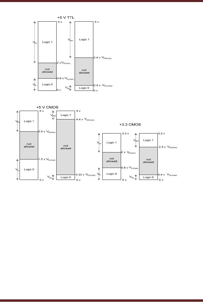
TTL are shown in the
figure 7.1. The VIH and VIL indicate the acceptable
voltage ranges for
the
input logic high and
low respectively. Similarly VOH and VOL indicate the acceptable
output
voltage
range for logic high
and low respectively.
61
CS302 -
Digital Logic & Design
Figure
7.1
Logic
Levels for TTL and
CMOS Series
a) TTL
Logic Levels
At the
input of any TTL logic
gate logic high `1' or a
logic low `0' signal is
applied.
· VIH is the input voltage
range of Logic high signal
with a range of 2 to 5
volts.
· VIH(min) is the minimum
acceptable input range for a
logic high signal. (2
volts)
· VIL is the input voltage
range of Logic low signal
with a range of 0 to 0.8
volts.
· VIL(max) is the maximum
acceptable input range for a
logic low signal. (0.8
volts)
The
output of any TTL logic
gate can be at logic high
`1' or logic low
`0'.
· VOH is the output voltage
range of Logic high signal
with a range of 2.4 to 5
volts.
· VOH(min) is the minimum
acceptable output range for
a logic high signal. (2.4
volts)
· VOL is the output voltage
range of Logic low signal
with a range of 0 to 0.4
volts.
· VOL(max) is the maximum
acceptable output range for
a logic low signal. (0.4
volts)
b) CMOS 5
Volt series Logic
Levels
At the
input of any CMOS 5 volt
series logic gate logic
high `1' or a logic low
`0' signal is
applied.
62

CS302 -
Digital Logic & Design
VIH is the input voltage
range of Logic high signal
with a range of 3.5 to 5
volts.
·
VIH(min) is the minimum
acceptable input range for a
logic high signal. (3.5
volts)
·
VIL is the input voltage
range of Logic low signal
with a range of 0 to 1.5
volts.
·
VIL(max) is the maximum
acceptable input range for a
logic low signal. (1.5
volts)
·
The
output of any CMOS 5 volt
series logic gate can be at
logic high `1' or logic
low `0'
· VOH is the output voltage
range of Logic high signal
with a range of 4.4 to 5
volts.
· VOH(min) is the minimum
acceptable output range for
a logic high signal.(4.4
volts)
· VOL is the output voltage
range of Logic low signal
with a range of 0 to 0.33
volts.
· VOL(max) is the maximum
acceptable output range for
a logic low signal. (0.33
volts)
c) CMOS
3.3 Volt series Logic
Levels
At the
input of any CMOS 3.3
volt series logic gate a
logic high `1' or a logic
low `0'
signal is
applied.
· VIH is the input voltage
range of Logic high signal
with a range of 2 to 3.3
volts.
· VIH(min) is the minimum
acceptable input range for a
logic high signal. (2
volts)
· VIL is the input voltage
range of Logic low signal
with a range of 0 to 0.8
volts.
· VIL(max) is the maximum
acceptable input range for a
logic low signal. (0.8
volts)
The
output of any CMOS 3.3
volt series logic gate
can be at logic high `1' or
logic low `0'
· VOH is the output voltage
range of Logic high signal
with a range of 2.4 to 3.3
volts
· VOH(min) is the minimum
acceptable output range for
a logic high signal. (2.4
volts).
· VOL is the output voltage
range of Logic low signal
with a range of 0 to 0.4
volts.
· VOL(max) is the maximum
acceptable output range for
a logic low signal. ( 0.4
volts).
The
valid output voltages
representing logic high and
low are confined to
certain
voltage
ranges. For example,
low-power 3.3 volt CMOS
chips output logic high
voltage ranges
between
2.4-3.3 volts and logic
low ranges between 0-0.4
volts. Output voltages that
are not
within
the specified ranges can
cause logic circuits to
malfunction.
A low-power
3.3v CMOS AND gate will
accept a voltage of 2.1
volts as a valid
logic
high
input. However, a voltage of
1.9 volts is unacceptable as an
input between 0.8-2.0
volts
will
give unpredictable results,
therefore input voltages
within this range is not
allowed.
Wires in
electronic circuits pick up
noise from adjacent
conductors. Noise is
unwanted
voltage
that is induced in the
circuit due to high-frequency
electromagnetic radiation.
The
unwanted
noise can affect the
performance of a logic gate
and the digital
circuit.
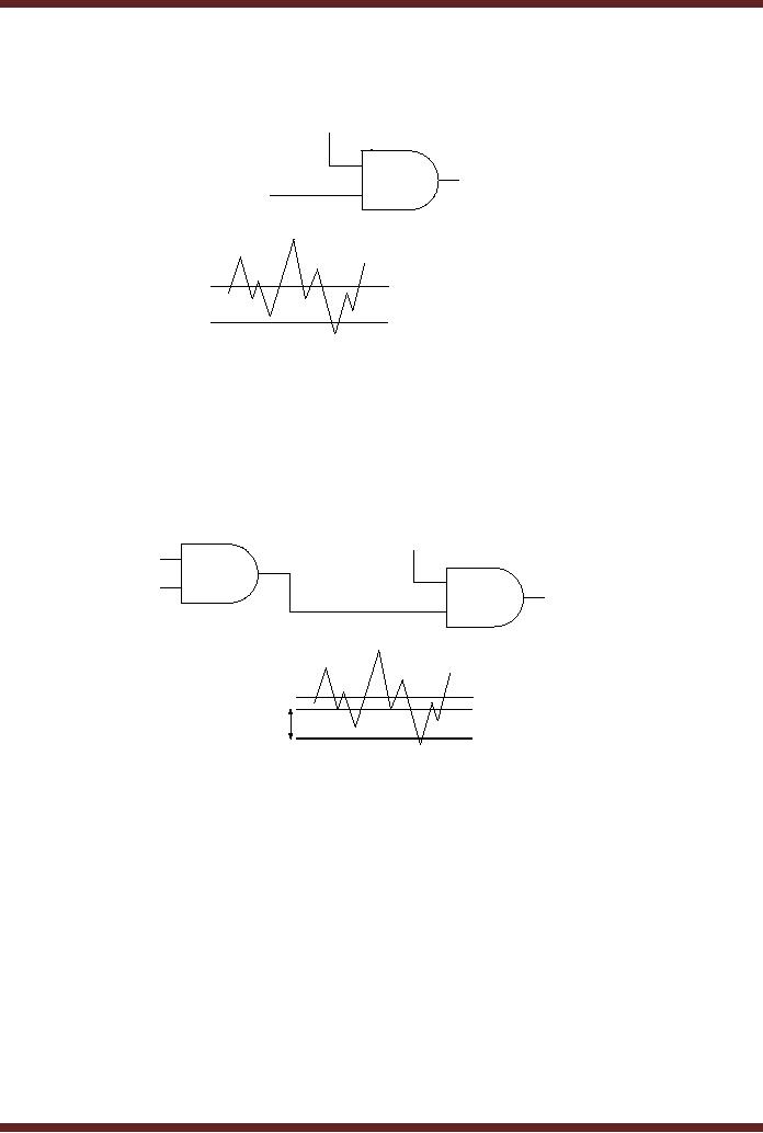
Effect of
Noise on the Operation of a
CMOS AND Gate
A CMOS 5
volt series AND gate is
shown. Figure 7.2. Input A
of the AND gate is
permanently
connected to logic high of +5
volts. Input B of the AND
gate is connected to
the
output of
some other gate. The
signal at input B of the AND
gate can vary between
logic 0 and
logic
1.
Consider
that the input B is at logic
High state with VIH = 4.2 volts which is
within the
valid
CMOS VIH
voltage
range of 5 to 3.5 volts. A
voltage generated due to
some external
noise
(shown by the zigzag line)
rides on the 4.2 volt
signal. A sharp dip in the
input voltage
due to
the noise brings the
input voltage down to 3
volts for a very short
duration. The 3 volt
input is
below the minimum input
voltage limit of 3.5 volts
for logic high input
voltage and within
63
CS302 -
Digital Logic & Design
the
not allowed voltage range.
This dip in the voltage
even for a short duration
will result in an
output of
logic low for a short
interval of time.
H
A
VIN
B
VIH = 4.2 v
VIH(min) = 3.5 v
EfVec= ofvNoise
on CMOS AND gate
f IH t 3
Figure
7.2
Effect of
Noise on the Operation of a
CMOS AND Gate
circuit
Two
CMOS 5 volt series AND gates
are connected together.
Figure 7.3 The first
AND
gate
has both its inputs
connected to logic high,
therefore the output of the
gate is guaranteed
to be logic
high. The logic high
voltage output of the first
AND gate is assumed to be 4.6
volts
well
within the valid VOH range of 5-4.4 volts.
Assume the same noise
signal (as described
earlier) is
added to the output signal
of the first AND
gate.
H
H
H
VOH = 4.6 v
VOH(min) = 4.4 v
VNH = 0.9 v
VIH(min) = 3.5 v
Noise
Margin High
Effect of
Noise VIn = 3.4OS AND gate circuit
oH CM v
Figure
7.3
The
sharp dip due to noise
brings the VOH voltage down to 3.4
volts with reference
to
the
VOH of 4.6 volts.
3.4 volts is lower than
the VIH(min) of 3.5 volts required by
the input of the
second AND
gate, the circuit will
thus malfunction.
Since
VOH(min)
is guaranteed to
be at 4.4 volts therefore a
noise signal being added
to
4.4
volts can bring VOH voltage down to a minimum of
3.5 volts which is the
acceptable
minimum
range for VIH.
Anything below 3.5 will
cause the second gate to
malfunction. Thus the
second AND
gate can tolerate a maximum
variation of 0.9 volts for
its logic high input or
has a
`Noise
Margin' of 0.9 volts.
Noise
Margin
Noise
margin is a measure of the
circuit's immunity to noise.
The high-level and
low-
level
noise margins are
represented by VNH
and VNL respectively.
64

CS302 -
Digital Logic & Design
·
VNH = VOH(min)
VIH(min)
·
VNL = VIL(max) VOL(max)
CMOS 5
volt series Noise
Margins
· VNH = VOH(min) VIH(min) = 4.4 - 3.5 = 0.9
v
· VNL = VIL(max) VOL(max) = 1.5 0.33 = 1.17
v
CMOS
3.3 volt series Noise
Margins
· VNH = VOH(min) VIH(min) = 2.4 2.0 = 0.4
v
· VNL = VIL(max) VOL(max) = 0.8 0.4 = 0.4
v
TTL 5
volt Noise Margins
· VNH = VOH(min) VIH(min) = 2.4 - 2.0 = 0.4
v
· VNL = VIL(max) VOL(max) = 0.8 0.4 = 0.4
v
The
CMOS 5 volts and the
3.3 volts series can
not be mixed.
For
CMOS 5 volt series the
high-level noise margin is
0.9 volts. That is,
the logic high
output of
the gate would never be
below 4.4 volts. Even if it
is below 4.4 volts due to
some
external
noise, the input will
consider any voltage above
3.5 volts to be logic high.
So CMOS 5
volt
series gates can withstand
noisy signals riding on
logic high inputs up to a
noise margin of
0.9
volts. Similarly, low-level
noise margin is 1.17 volts
(1.5-0.33).
The
VNH high-level and
VNL low-level noise
margins for TTL 5 volt
and CMOS 3.3
series
are
0.4 volts and 0.4
volts respectively. Therefore in
noisy environments, CMOS 5
volt series
based
digital system perform
better.
3. Power
Dissipation
Logic
Gates and Logic circuits
consume varying amount of
power during their
operation.
Ideally, logic gates and
logic circuit should consume
minimal power. Advantages
of
low
power consumption are
circuits that can be run
from batteries instead of
mains power
supplies.
Thus portable devices that
run on batteries use
Integrated circuits that
have low
power
dissipation. Secondly, low
power consumption means less
heat is dissipated by
the
logic
devices; this means that
logic gates can be tightly
packed to reduce the circuit
size
without
having to worry about
dissipating the access heat
generated by the logic
devices.
Microprocessors
for example generate
considerable heat which has
to be dissipated by
mounting
small fans.
Generally,
the Power dissipation of TTL
devices remains constant
throughout their
operation.
CMOS device on the other
hand dissipate varying
amount power depending
upon
the
frequency of operation.
a) Power
Dissipation of TTL
Devices
When a
TTL logic gate output is in
a logic high state it draws
out a current from the
dc
power
supply. It is said to be sourcing
current. The high current is
designated by ICCH,
typical
value
for ICCH is 1.5 mA when VCC = 5 V. When a TTL logic
gate output is in a logic
low state it
sinks a
current designated by ICCL = 3.0 mA when
VCC = 5 V. The figure
7.4 shows an AND
gate
connected to output a logic
high `1'. It thus draws a
current ICCH from the voltage
supply
VCC.
65
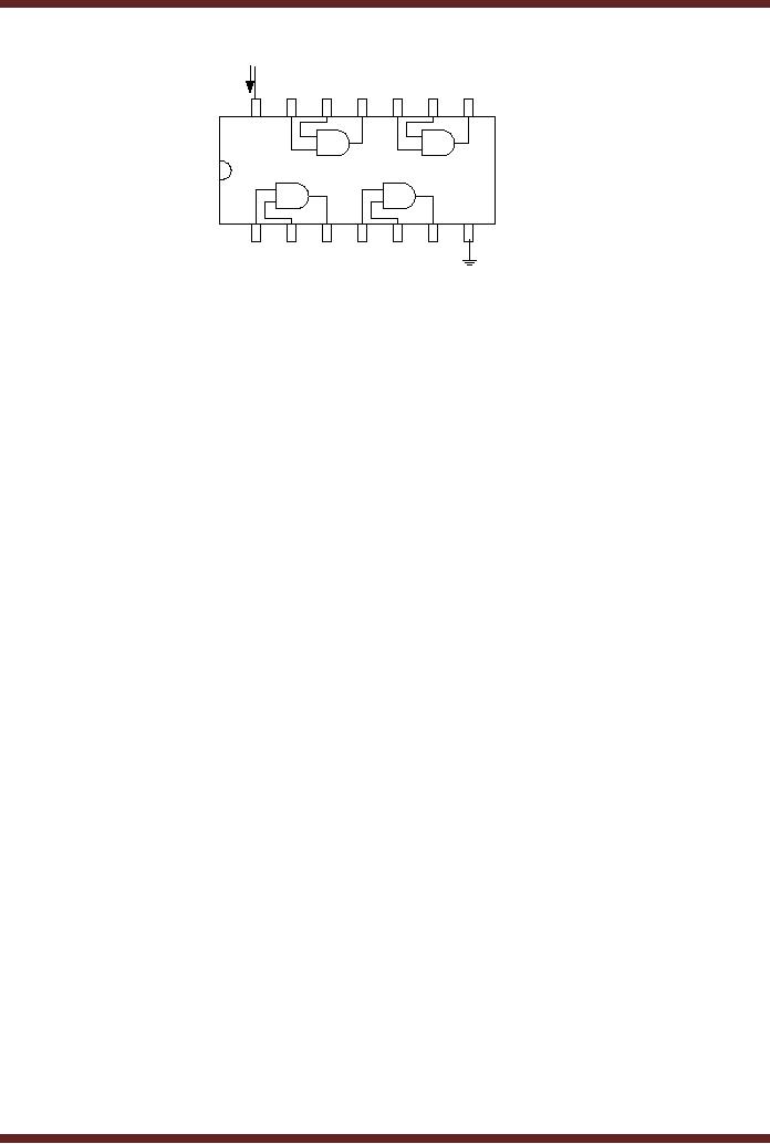
CS302 -
Digital Logic & Design
+5 v
+5 v +5 v
ICCH
8
12
11
13
10
9
14
1
2
3
4
5
6
7408
Four
2-Input AND Gate
Figure
7.4
Power
dissipation of a TTL AND
gate
When
any one of the AND gate
input is connected to low,
the output becomes low
and
it sinks
current ICCL. An
AND Gate which has one of
its input connected to a
clock which
continuously
changes from logic high to
low sets the AND gate
output to high and
low
respectively
for every one half of
the clock cycle. Thus
the AND gate sources and
sinks
currents
ICCH and ICCL respectively.
The
power dissipated by a gate is
VCC x ICC. The
power dissipated would be
different
for a
gate having a logic high
output and logic low
output. The average power
dissipated is
determined,
based on a 50% duty cycle,
that is, the gate is
pulsed and its output
switches
between
high and low for
every one half of the
cycle.
PD = VCC(ICCH +
ICCL)/2
Power
Dissipation in TTL circuits is
constant over its range of
operating frequencies.
For
example, the power
dissipation of a LS TTL gate is a
constant 2.2 mW.
b) Power
Dissipation of CMOS
Devices
The
transistors used in CMOS
logic present a capacitive
load instead of the
resistive
load in
TTL based logic. Each
time a CMOS logic gate
switches between low and
high, current
has to be
supplied to the capacitive
load. The typical supply
current is 5 mA for a duration
of
20-30
nsec. As the frequency of
operation increases, there
would be more of these
current
spikes
occurring per second, thus
the average current drawn
from the voltage
source
increases.
Power
Dissipation in CMOS circuits is
frequency dependent. It is extremely
low under
static
(dc) conditions and
increases as the frequency
increases. Total Dynamic
Power
dissipation of a
CMOS circuit is
PD = PT + PL
where
PT is the internal
power dissipation of the
gate
PL is the external power
dissipation due to the
external capacitive
load
PD = CPD.VDD2.f
+ CL.VDD2.f
PD = (CPD+ CL).VDD2.f
where
CPD is the internal
power dissipation
capacitance
CL is the external load
dissipation capacitance
VDD is the supply
voltage
f is the
transition frequency of the
output signal
66
CS302 -
Digital Logic & Design
The
power dissipation of a HCMOS
gate is 2.75 μW under
static conditions and 170
μW at
100
KHz.
4. Propagation
Delay
When
ever a signal passes through
a gate it experiences a delay.
That is, a signal
applied to
the input of a gate does
not result in an instantaneous
response. The output of
a
gate is
delayed with respect to the
input. The delay in the
output is known as the
Propagation
Delay.
The
Propagation Delay of a gate
limits the frequencies at
which the gate can
work.
Higher
the Propagation Delay lower
is the frequency at which
the gate can operate.
Smaller
the
Propagation Delay higher the
frequency at which the gate
can operate. A Gate with
a
Propagation
Delay of 3 nsec is faster
than a gate with a 10 nsec
delay.
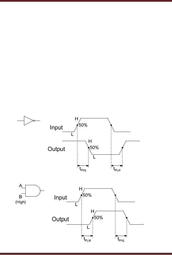
There
are two Propagation Delay
times specified for Logic
Gates. Figure 7.5
·
tPHL The time
between a specified reference
point on the input pulse
and a corresponding
reference
point on the resulting
output pulse, with the
output changing from high
level to
low
level.
·
tPLH The time
between a specified reference
point on the input pulse
and a corresponding
reference
point on the resulting
output pulse, with the
output changing from low
level to
high
level.
Figure
7.5
Propagation
delay of an NOT & AND
gates
67

CS302 -
Digital Logic & Design
The
output of the NOT gate
changes from high to low
after a delay of time
specified by
tPHL after the
input changes from low to
high. The output of the
NOT gate changes from
low to
high
after a delay of time
specified by tPLH after the input
changes from high to low.
The delay
time is
measured at the 50%
transition mark.
The
input B of the AND gate is
permanently connected to logic
high, where as input
A
varies
between High and Low.
The output of the AND gate
changes from low to high
after a
delay of
time specified by tPLH after the input
changes from low to high.
The output of the AND
gate
changes from high to low
after a delay of time
specified by tPHL after the input
changes
from
high to low. The delay
time is measured at the 50%
transition mark. Generally,
the tPLH
and
tPHL propagation delay
times are same.
The
effect of Propagation Delay on
the operation of a digital
circuit can be
explained
with
the help of an example.
Consider a Cricket Stadium,
entry to the Cricket Stadium
is
through
three gates, each manned by
a security guard who allows
the spectator into
the
stadium
after checking the ticket.
Assume that the security
guards at Gates A, B and C
take 1,
1.5
and 2 minutes respectively to
check the ticket and
allow the spectator into
the stadium.
Assuming
equal number of spectators
queuing up at the three
gates, the queue at gate C
after
30 minutes is
the longest as the guard at
Gate C has the longest
Propagation Delay.
5. Speed-Power
Product (SPP)
An important
parameter is the Speed-Power
Product which is used as a
measure of
performance of a
logic circuit taking into
account the propagation
delay and the
power
dissipation.
The
SPP = tPPD expressed in Joules (J),
the unit of energy. Lower
the SP product better is
the
performance.
6. Fan-Out
and Loading
The
fan-out of a logic gate is
the maximum numbers of
inputs of the same series in
an
IC family
that can be connected to a
gate's output and still
maintain the output voltage
levels
within
the specified limits.
Fan-out parameter is associated
with TTL technology.
CMOS
circuits
have very high impedance
therefore fan-out of CMOS
circuits is very high but
depends
upon
the frequency because of
capacitance effects.
Fan-out is
specified in terms of unit
loads. A unit load for a
logic gate equals one
input
to a like
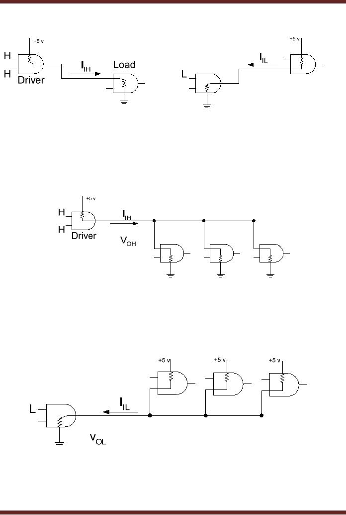
circuit. Consider a 7400 NAND
gate. The output current at
logic high is IOH =
400 μA.
The
input current at logic high
is IIH = 40 μA. Thus a
gate at logic high can
source current to
another
gate connected to its
output.
Similarly,
the output current at logic
low is IOL
= 16 mA.
The input current at logic
low is
IIL = 1.6 mA. Thus a
gate output at logic low
can sink current from
another gate connected
to
its
output.
Unit
Loads = IOH/IIH = IOL/IIL =
400 μA/40
μA = 16 mA/1.6 mA
= 10
68
CS302 -
Digital Logic & Design
Figure
7.6
AND Gate
Sourcing and Sinking
Current
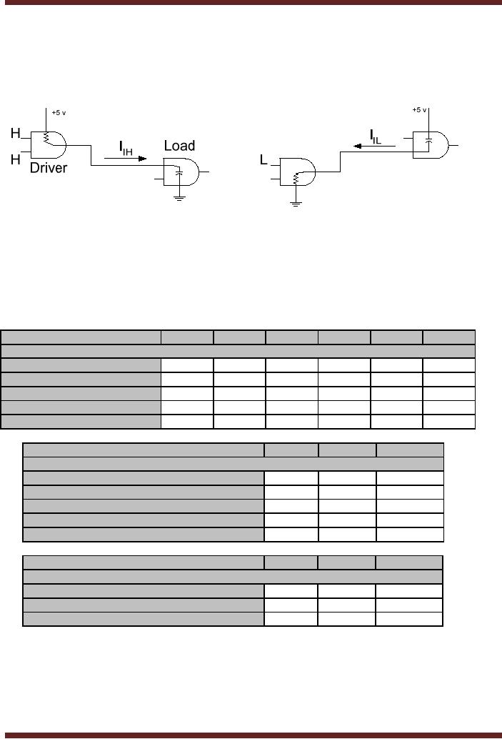
As more
gates (Loads) are connected
to the driving gate the
loading on the
driving
gate
increases. The total current
sourced by the driving gate
increases. As the
current
increases
the internal voltage drop
increases causing the output
voltage VOH
to decrease.
If
excessive
number of gates are
connected the output voltage
VOH drops below
the VOH(min)
reducing
the High-level noise margin,
thus compromising the
circuit operation. Also as
the
source
current increases the power
dissipation increases. Figure
7.7.
Figure
7.7
AND Gate
Sourcing Current
The
total sink current also
increases with each load
gate that is added. As the
sink
current
increases the internal
voltage drop of the driving
gate increases causing VOL to
increase. If
excessive number of loads
are connected, VOL exceeds VOL(max) and the Low
noise
margin is
reduced.
Figure
7.8
AND Gate
Sinking Current
CMOS
loading is different from
TTL loading as the type of
transistors used in
CMOS
circuits
presents a capacitive load to
the driving gate. When
the output of the driving
gate is
high
the input capacitance of the
load gate is charging and
when the output of the
driver gate
69
CS302 -
Digital Logic & Design
is low
the load gate is
discharging. When more load
gates are added the
input capacitance
increases as
input capacitances are being
connected in parallel. With
the increase in the
capacitance,
charging and discharging
time increases, reducing the
maximum frequency at
which
the gate can operate.
Figure 7.9
Figure
7.9
CMOS AND
Gate Sourcing and Sinking
Current
The
fan-out of a CMOS gate
depends upon the maximum
frequency of operation.
Fewer
the load gates, greater
the maximum frequency of
operation.
Different
TTL series are characterized
by switching speed and power
consumption as
shown in
the table. Table
7.1
74
74S
74LS
74AS
74ALS
74F
Performance
Rating
Propagation
Delay (ns)
9
3
9.5
1.7
4
3
Power
Dissipation (mW)
10
20
2
8
1.2
6
Speed-Power
product (pJ)
90
60
19
13.6
4.8
18
Max.
Clock Rate (MHz)
35
125
45
200
70
100
Fan-out
(same series)
10
20
20
40
20
33
74HC
74AC
74AHC
Performance
Rating
Propagation
Delay (ns)
18
5
3.7
Power
Dissipation (mW)
Static
0.00275
0.0055
0.00275
Power
Dissipation (mW) Dynamic
100KHz
0.0625
0.08
0.0625
Speed-Power
product (pJ) at
100KHz
1.125
0.4
0.23
Max.
Clock Rate (MHz)
50
160
170
74LV
74LVC
74ALVC
Performance
Rating
Propagation
Delay (ns)
9
4.3
3
Power
Dissipation (mW)
Static
0.0016
0.0008
0.0008
Max.
Clock Rate (MHz)
90
100
150
Table
7.1
Operational
Characteristics of TTL and
CMOS families
70
Table of Contents:
- AN OVERVIEW & NUMBER SYSTEMS
- Binary to Decimal to Binary conversion, Binary Arithmetic, 1s & 2s complement
- Range of Numbers and Overflow, Floating-Point, Hexadecimal Numbers
- Octal Numbers, Octal to Binary Decimal to Octal Conversion
- LOGIC GATES: AND Gate, OR Gate, NOT Gate, NAND Gate
- AND OR NAND XOR XNOR Gate Implementation and Applications
- DC Supply Voltage, TTL Logic Levels, Noise Margin, Power Dissipation
- Boolean Addition, Multiplication, Commutative Law, Associative Law, Distributive Law, Demorgans Theorems
- Simplification of Boolean Expression, Standard POS form, Minterms and Maxterms
- KARNAUGH MAP, Mapping a non-standard SOP Expression
- Converting between POS and SOP using the K-map
- COMPARATOR: Quine-McCluskey Simplification Method
- ODD-PRIME NUMBER DETECTOR, Combinational Circuit Implementation
- IMPLEMENTATION OF AN ODD-PARITY GENERATOR CIRCUIT
- BCD ADDER: 2-digit BCD Adder, A 4-bit Adder Subtracter Unit
- 16-BIT ALU, MSI 4-bit Comparator, Decoders
- BCD to 7-Segment Decoder, Decimal-to-BCD Encoder
- 2-INPUT 4-BIT MULTIPLEXER, 8, 16-Input Multiplexer, Logic Function Generator
- Applications of Demultiplexer, PROM, PLA, PAL, GAL
- OLMC Combinational Mode, Tri-State Buffers, The GAL16V8, Introduction to ABEL
- OLMC for GAL16V8, Tri-state Buffer and OLMC output pin
- Implementation of Quad MUX, Latches and Flip-Flops
- APPLICATION OF S-R LATCH, Edge-Triggered D Flip-Flop, J-K Flip-flop
- Data Storage using D-flip-flop, Synchronizing Asynchronous inputs using D flip-flop
- Dual Positive-Edge triggered D flip-flop, J-K flip-flop, Master-Slave Flip-Flops
- THE 555 TIMER: Race Conditions, Asynchronous, Ripple Counters
- Down Counter with truncated sequence, 4-bit Synchronous Decade Counter
- Mod-n Synchronous Counter, Cascading Counters, Up-Down Counter
- Integrated Circuit Up Down Decade Counter Design and Applications
- DIGITAL CLOCK: Clocked Synchronous State Machines
- NEXT-STATE TABLE: Flip-flop Transition Table, Karnaugh Maps
- D FLIP-FLOP BASED IMPLEMENTATION
- Moore Machine State Diagram, Mealy Machine State Diagram, Karnaugh Maps
- SHIFT REGISTERS: Serial In/Shift Left,Right/Serial Out Operation
- APPLICATIONS OF SHIFT REGISTERS: Serial-to-Parallel Converter
- Elevator Control System: Elevator State Diagram, State Table, Input and Output Signals, Input Latches
- Traffic Signal Control System: Switching of Traffic Lights, Inputs and Outputs, State Machine
- Traffic Signal Control System: EQUATION DEFINITION
- Memory Organization, Capacity, Density, Signals and Basic Operations, Read, Write, Address, data Signals
- Memory Read, Write Cycle, Synchronous Burst SRAM, Dynamic RAM
- Burst, Distributed Refresh, Types of DRAMs, ROM Read-Only Memory, Mask ROM
- First In-First Out (FIFO) Memory
- LAST IN-FIRST OUT (LIFO) MEMORY
- THE LOGIC BLOCK: Analogue to Digital Conversion, Logic Element, Look-Up Table
- SUCCESSIVE APPROXIMATION ANALOGUE TO DIGITAL CONVERTER