 |
Burst, Distributed Refresh, Types of DRAMs, ROM Read-Only Memory, Mask ROM |
| << Memory Read, Write Cycle, Synchronous Burst SRAM, Dynamic RAM |
| First In-First Out (FIFO) Memory >> |
CS302 -
Digital Logic & Design
Lesson
No. 41
READ AND
WRITE CYCLES
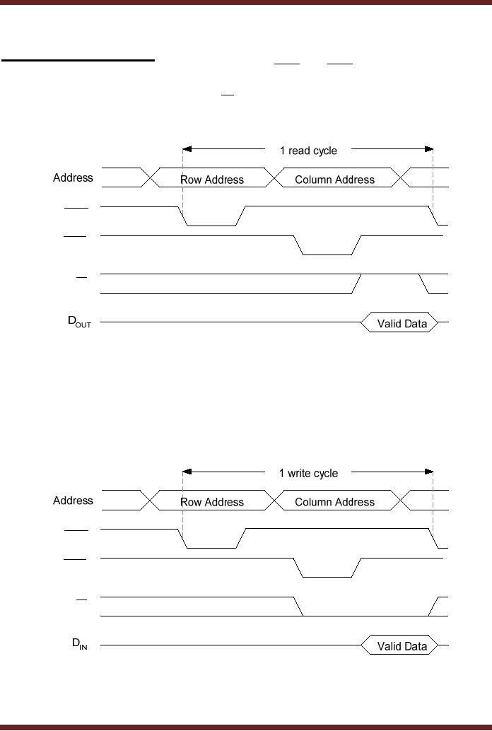
The
read cycle is shown. Figure
41.1a. The RAS and CAS signals are activated
one
after
the other to latch the
multiplexed row and column
addresses respectively applied at
the
multiplexed
address input lines. The
R / W signal is
activated to read data which
is made
available on
the DOUT data line.
RAS
CAS
R/W
Figure
41.1a DRAM Read Cycle
The
write cycle is similar to
the read cycle. Figure
41.1b. The row and
column
addresses
are applied at the
multiplexed address inputs
along with the strobe
signals that
latch
the row and column
addresses in the row and
column address latches
respectively. The
write
signal is activated allowing
data placed at the DIN data line to be stored in
the selected
memory
cell.
RAS
CAS
R/W
Figure
41.1b DRAM Write
Cycle
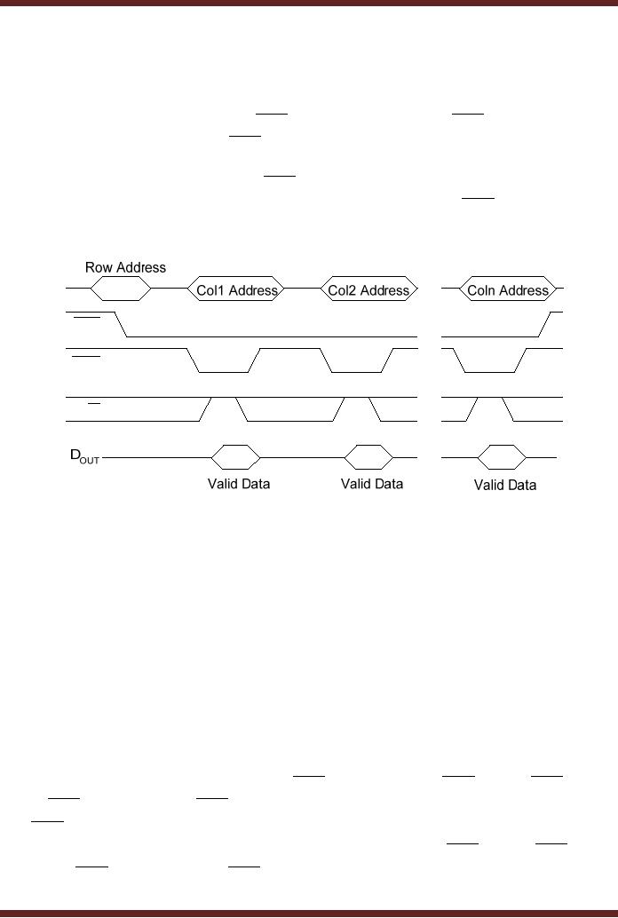
FAST
Page Mode
412
CS302 -
Digital Logic & Design
In a FAST
Mode Page Access all
the columns in the same
row are either read
or
written. A
single row is considered to be a
`Page' of memory storing
data values in
successive
memory
locations. The FAST Mode
Page Access allows faster
memory read and access
times
when
reading successive data
values stored in consecutive
locations on the same row.
The
row
address is first latched by
the RAS signal going low.
The RAS signal remains
low
throughout
the Page Access. The
CAS signal is toggled
between high and low
which selects
successive
columns in the selected row.
Data is read or written to
successive column
locations.
During the read cycle
when CAS goes high the DOUT line is disabled.
Therefore,
data on
the DOUT line has to be latched by
the external system before
CAS goes high.
Figure
41.2.
RAS
CAS
R/W
Figure
41.2
FAST
Page Mode Read
Cycle
Burst
Refresh and Distributed
Refresh
DRAM chips
are refreshed using either
the Burst Refresh Mode or
the Distributed
Refresh
Mode. In the Burst Refresh
Mode, all rows in the DRAM
chip are refreshed
consecutively in
each refresh cycle. For a
DRAM having a refresh cycle of 8
msec, a burst
refresh of
all rows occurs once
every 8 msec. During the
refresh cycle the memory
can not be
accessed
for normal read and
write operations, therefore
the read/write operations
are
suspended
until the refresh cycle is
completed.
In Distributed
Mode, the refresh cycle is
interspersed between normal
read and write
cycles.
For the 1024 x 1024 DRAM
memory and a refresh cycle
of 8 msec, each of the
1024
rows
has to be refreshed in 7.8
microsec when Distributed
refresh is used.
RAS only
Refresh and CAS before RAS
Refresh
The
refresh cycles are of two
types, RAS only refresh and CAS before RAS refresh.
In the
RAS only refresh
the RAS signal goes low
latching the row address to
be refreshed,
the CAS signal remains
inactive high throughout the
refresh cycle. An external
counter is
used to
provide the row addresses
for the refresh operation.
In the CAS before RAS refresh
mode,
the CAS goes low before RAS goes low.
This sequence activates an
internal refresh
413

CS302 -
Digital Logic & Design
counter
that generates the row
address to be refreshed. This
address is switched by the
data
selector
into the row
decoder.
Types of
DRAMs
There
are several different types
of DRAMS available.
· Fast
Page Mode DRAM: Compared to
random access read/write,
FAST Page Mode is
faster
where successive columns on
the same row are
read/written in successively by
asserting
the CAS strobe signal. The
CAS signal when
de-asserted, disables the DOUT
data
line, therefore the next
column address can not
occur unless the data at
the current
address is
latched by the external
system reading data from
the DRAM. The access
speed
of the DRAM
during read operation is
therefore limited by the
external system latching
the
data
available on the DOUT line.
· Extended
Data Output (EDO) DRAM:
The memory in its operation
is similar to the FPM
DRAM,
however the CAS signal doesn't disable
the DOUT when it goes to its
non-asserted
state.
Thus the valid data on
the DOUT line can be remain
until the CAS signal is asserted
again to
access the next column.
Thus the next column
address can be accessed
before
the
external system accepts the
current data.
·
Synchronous
DRAM: The DRAM operations
are tied to a clock signal
that also times
the
microprocessor
operations. This allows the
DRAM to closely synchronize with
the
microprocessor.
ROM
Read-Only Memory
A ROM contains
permanent data that can
not be changed. Thus ROM
memory does
not
allow write operation. A ROM
stores data that are
used repeatedly in system
applications,
such as
tables, conversions, programmed
instructions for system
initialization and
operation.
ROMs
retain data when the
power is turned off. ROMs
are of different
types.
· Mask
ROM: Data is permanently
stored during the
manufacturing process.
· PROM:
Programmable ROM allows storage of
data by the user using a
PROM
programmer.
The PROM once programmed
stores the data
permanently.
· EPROM:
Erasable PROM allows erasing
of stored data and
reprogramming.
· UV EPROM:
Is a programmable ROM. Data is
erased by exposing the PROM
to Ultraviolet
light.
· EEPROM:
Electrically Erasable PROM is
erased electrically. EEPROM
allows in-circuit
programming
and doesn't need to be
removed from the circuit
for erasure or
programming.
Mask
ROM
The
structure of a storage cell in a
Mask ROM is shown. Figure
41.3. The storage
cell
in a Mask ROM is
implemented using a MOS transistor.
The Gate of the transistor
is
connected to
the row line and
the output of the transistor
is connected to the column
line.
When a
row is selected all the MOS
transistors with their Gates
connected to the row
are
turned on
and connect their high
output to their respective
column line. Transistors
with their
GATE
connections to the row
removed are not turned on
and the corresponding column
lines
have a
logic low output. During
the manufacturing process
the cells that store
logic one have
the
transistors configured with
their Gates intact and
cells having logic 0 have
the transistors
configured
with their Gate connections
removed.
414
CS302 -
Digital Logic & Design
Column
Column
Row
Row
+VDD
+VDD
Figure
41.3
ROM cell
storing a logic 1 and logic
0
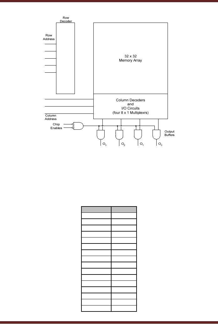
Address
Decoder
Row
0
0
Row
1
1
Address
Input
Lines
Row
2
2
Row
14
14
Row
15
15
Terminating
Resistors
Data
Output
0
1
2
6
7
Lines
Figure
41.4
General
Architecture of a ROM
A 16 x 8 ROM is
shown. Figure 41.4. A 4-bit
address is decoded by a 4 x 16
decoder
which
selects the appropriate row
line. The MOSFETs connected
to the selected row
output
logic 1 on
the respective column lines.
The MOSFETs that are
not connected output logic
0.
The
terminating resistor connected to
the end of each column
line ensures that the
output line
stays
low when a MOSFET outputs
logic 0.
The
Internal Structure of Mask ROM
chip is different from the
simplified structure
shown in
figure 41.4. A 256 x 4 ROM
device is organized in the
form of a 32 x 32 row-column
structure.
The 8-bit address is split
into a 5-bit row address
which selects one out of
the 32
rows
and the remaining 3 bits
are used to select 1 out of
8 column lines by four 8 x
1
Multiplexers.
Figure 41.5.
415
CS302 -
Digital Logic & Design
Figure
41.5
Internal
structure of a 264 x 4 ROM
ROM
Applications
The
264 x 4 ROM can be used as
conversion table to convert
4-bit binary values to
4-
bit
equivalent Gray Code values.
The 4-bit code which is to
be converted is applied as an
address at
the 4-bit address input of
the ROM. At each of the
256 locations corresponding
to
the
256 addresses 256 Gray
Code values are stored.
The 4-bit Gray Code
contents stored at
the
first 16 locations of the ROM
are shown. Table 41.1. ROM
can also be used as a
simple
table.
Each location in the ROM
stores a value which can be
accessed by specifying
the
location
address. Look-Up tables used
in computers can be implemented
using ROMs.
Address
Data
0000
0000
0001
0001
0010
0011
0011
0010
0100
0110
0101
0111
0110
0101
0111
0100
1000
1100
1001
1101
1010
1111
1011
1110
1100
1010
1101
1011
1110
1001
1111
1000
Table
41.1
ROM programmed
to convert 4-bit Binary to
4-bit Gray Code
416
CS302 -
Digital Logic & Design
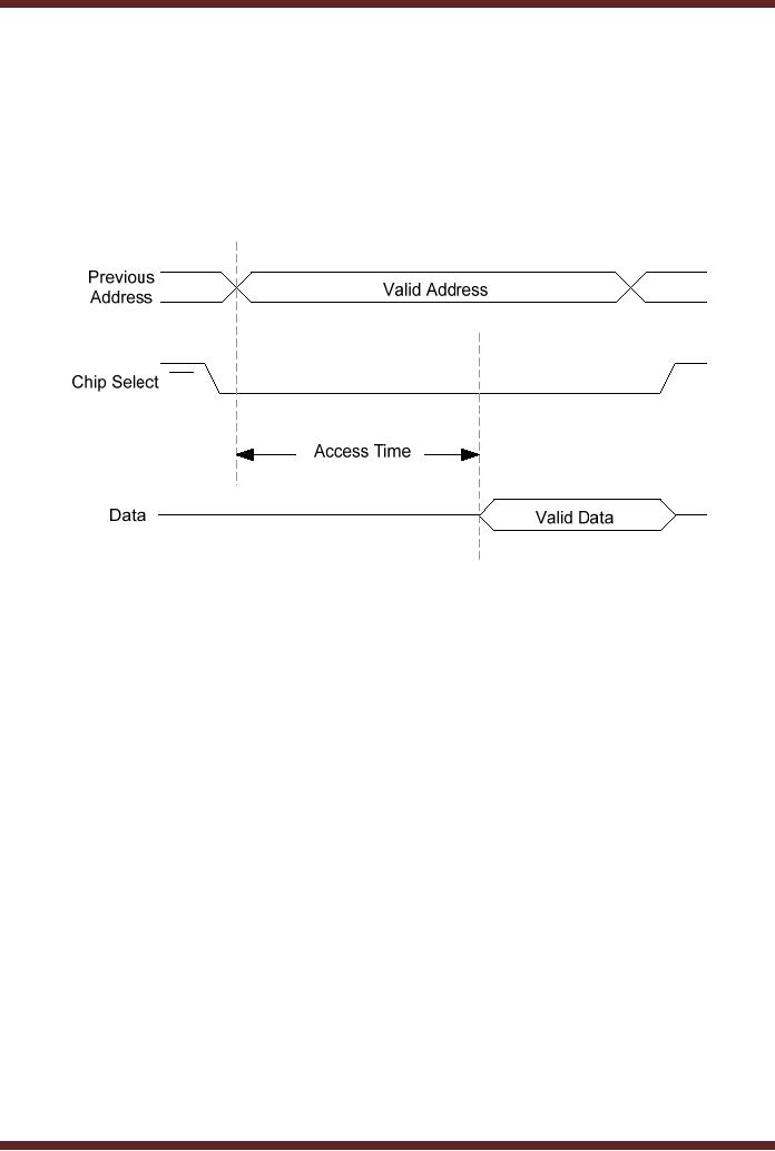
ROM
Read Cycle & Access
Time
The
Access Time of a ROM is the
time it takes for the
data to appear at the
Data
Output of
the ROM chip after an
address is applied at the
address input lines. The
access time
can
also be measured with
respect to the activation of
the chip enable signal
and the
appearance of
the data at the output
lines when address is
already on the address
lines.
Figure
41.6.
CS
Figure
41.6
Read
Access Time of a ROM
chip
PROM
(Programmable ROMs)
The
Mask ROM are programmed at
the manufacturing time and
can not e programmed
by the
user. Mask ROM allows
read-only operation. A PROM
can be programmed once by
the
user
using a PROM Programmer.
Once the PROM is programmed
its contents can not
be
erased
and programmed again. PROM
uses a fusible link to
connect the output of the
MOS
transistors to
the column line. The
row lines are permanently
connected the gates of
the
transistors.
When the fuse is intact,
logic high is seen on the
column line when
the
corresponding
cell is selected. When the
fuse is blown the column
line outputs a logic
low.
Figure
41.7.
417
CS302 -
Digital Logic & Design
Figure
41.7
PROM
array with fusible
links
EPROM
Erasable PROM
An EPROM is an
Erasable PROM. The contents
of the memory can be erased
and the
memory
can be reprogrammed. The
EPROM uses NMOSFET array
with an isolated-gate
structure.
The isolated gate structure
can store a charge for
indefinite periods of time.
The
data
bits are represented by the
presence or absence of gate
charges. Erasure of data bit
is
the
removal of gate
charge.
Two
basic types of EPROMs are
the Ultra Violet EPROM (UV
EPROM) and the
Electrically
Erasable EPROM (EEPROM). In
the UV EPROM, the
programming process
causes
the electrons to be removed
from the isolated gate.
The UV EPROM has a
quartz
window on
the package through which
the memory array is exposed
to high-intensity UV
which
causes the positive charge
stored on the gate to
neutralize after an exposure
time of
few
minutes. A typical UV EPROM
memory chip is shown. Figure
41.8
CE / PGM
OE
418

CS302 -
Digital Logic & Design
Figure
41.8
A 2 KB
EPROM
The 2
KByte EPROM has 2K locations
each storing a byte data
value. Addressing 2K
locations
requires 210
or 10 address
lines A0
to A10. Each memory location
stores a byte value,
therefore 8
data lines are required. To
read data from the
EPROM, the chip has to be
selected
by setting
the chip enable/program CE / PGM signal to
active-low and the output
enable OE
is
set to
logic low.
Programming
EPROM
Programming
the EPROM chip is done by
applying a high dc voltage at
the VPP pin
and
setting
the output enable OE to logic high. The
data to be programmed is applied at
the eight
data
lines and the address at
which the data is to be
programmed is applied at the
address
lines. A
high level pulse is applied
at the enable/program CE / PGM signal to program
the data
at the
required address. The entire
EPROM is programmed by applying
data values at the
data
lines the corresponding
address at the address input
lines and high level
pulses at the
CE / PGM pin.
EEPROM
Electrically Erasable
PROM
An electrically
erasable PROM is programmed
and erased by applying
electric pulses.
Since
this PROM does not
need to be exposed to Ultra
Violet light for erasing
data therefore
the
EEPROM can be rapidly
programmed and erased
in-circuit.
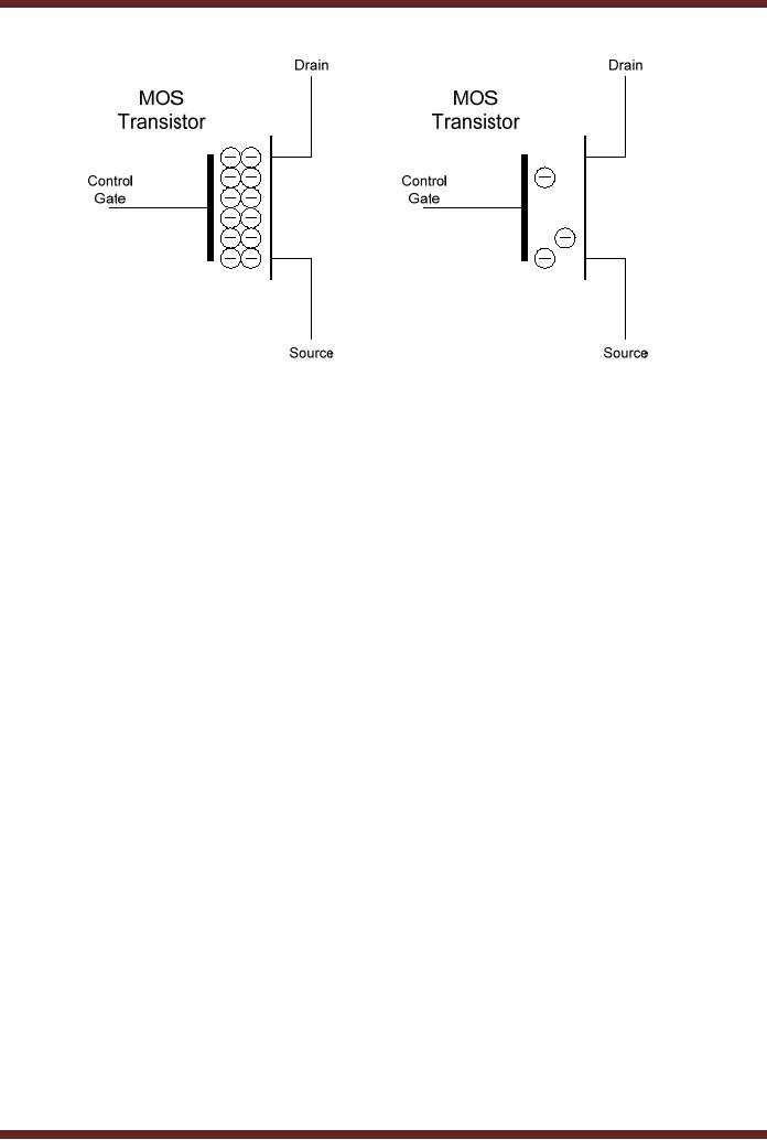
FLASH
Memory
An ideal
memory should have high
density, have read/write
capability, should be
non-
volatile,
have fast access time
and should be cost
effective. The ROM, PROM,
EPROM,
EEPROM, SRAM
and DRAM all exhibit some of
these characteristics, however
none of these
memories
have all the mentioned
characteristics except for
the FLASH Memory.
FLASH
memories have high density,
that is, they store
more information per unit
area
as more
storage cells are
implemented per unit area.
These memories have
read/write
capability
and are non-volatile and
can store data for
indefinite time period. The
high density
FLASH
memory cell is implemented
using a single floating-gate MOS
transistor. A data bit
is
stored as a
charge (logic 0) or the
absence of a charge (logic 1) on
the floating gate.
The
amount of
charge present o the
floating gate determines if
the transistor will turn
and conduct
current
from the drain to the
source when a control
voltage is applied at the
Control rate during
the
read operation. Figure
41.9
419
CS302 -
Digital Logic & Design
Figure
41.9
MOS transistor
with charge (logic 0) and no
charge (logic 1)
FLASH
Memory Operations
FLASH
Memory operations are
classified into
· Programming
Operation
· Read
Operation
· Erase
Operation
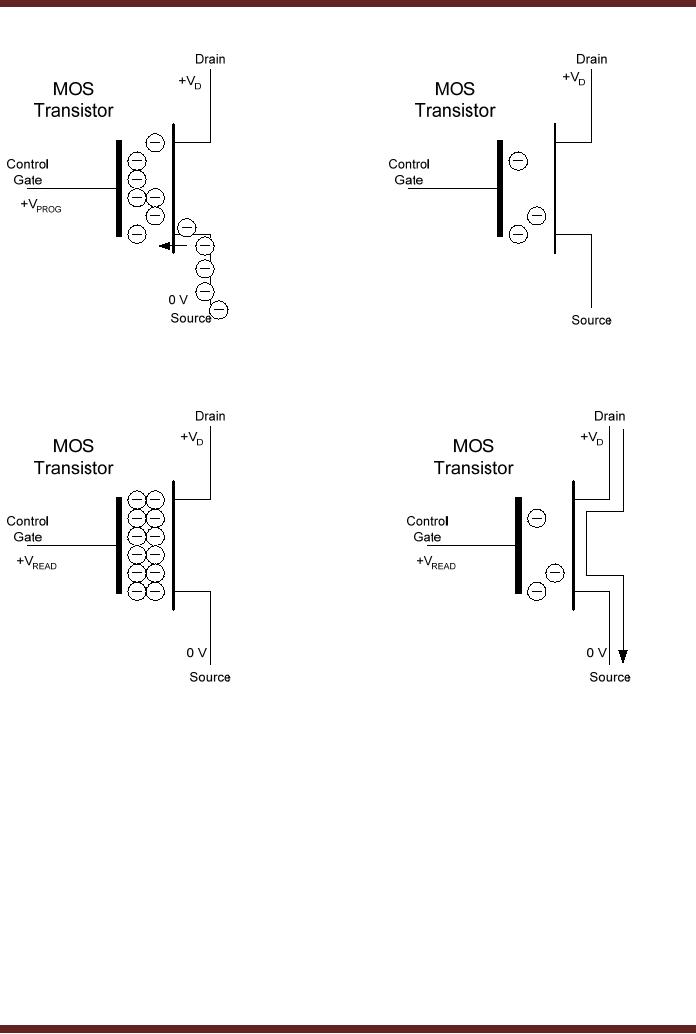
Programming
Operation
Initially,
all cells are at the
logic 1 state, that is with
no charge. The
programming
Operations
adds charge to the floating
gate of those cells that
are to store a logic 0. No
charge
is added to
those gates that are to
store a logic 1. The charges
are stored by applying
a
positive
voltage at the Control Gate
with respect to the Source
which attracts electrons to
the
floating
gate. Once the gate is
charged it, retains the
charge for years. Figure
41.10
Read
Operation
During
the read operation a
positive voltage is applied to
the MOS transistor
control
gate. If a
negative charge is stored on
the gate then the
positive read voltage is not
sufficient
to overcome
the negative charge
therefore the transistor is
not turned on. On the
other hand if
there is no or
small amount of negative
charge stored, the positive
read voltage is sufficient
to
overcome
the negative charge turning
on the transistor. When the
transistor is turned on
there
is a current
from the drain to the
source of the cell
transistor. The presence of
this current is
sensed to
indicate a 1. The absence of
this current indicates a 0.
Figure 41.10.
420
CS302 -
Digital Logic & Design
Figure
41.10 FLASH Memory Cell
programmed with logic 0 and
logic 1
Figure
41.11 Read operation to read
a logic 0 and a logic
1
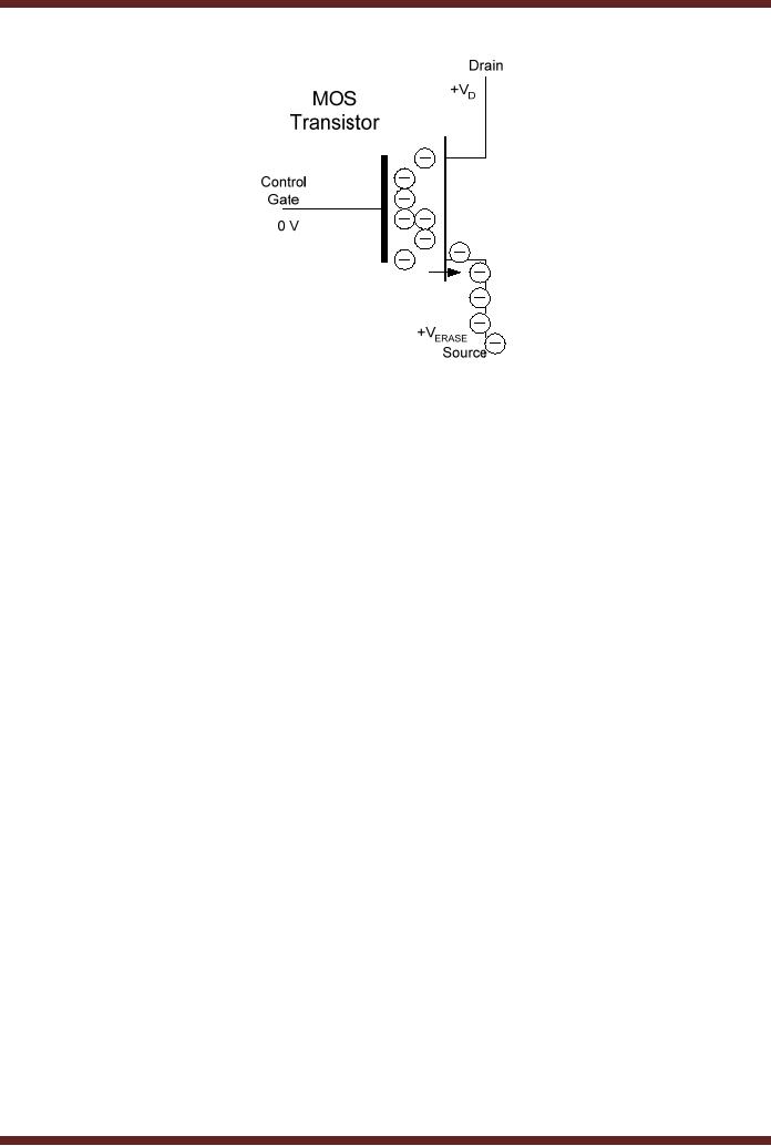
Erase
Operation
During
the erase operation charge
is removed from the memory
cell. A sufficiently
large
positive voltage is applied at
the source with respect to
the control gate. The
voltage
applied
across the control gate
and source is opposite to
the voltage applied
during
programming. If
charges are present on the
gate, the positive voltage
supply at the source
attracts
the electrons depleting the
gate. A FLASH memory is
erased prior to
programming.
Figure
41.12
421
CS302 -
Digital Logic & Design
Figure
41.12 The Erase Operation of
the FLASH Memory
Cell
422
Table of Contents:
- AN OVERVIEW & NUMBER SYSTEMS
- Binary to Decimal to Binary conversion, Binary Arithmetic, 1s & 2s complement
- Range of Numbers and Overflow, Floating-Point, Hexadecimal Numbers
- Octal Numbers, Octal to Binary Decimal to Octal Conversion
- LOGIC GATES: AND Gate, OR Gate, NOT Gate, NAND Gate
- AND OR NAND XOR XNOR Gate Implementation and Applications
- DC Supply Voltage, TTL Logic Levels, Noise Margin, Power Dissipation
- Boolean Addition, Multiplication, Commutative Law, Associative Law, Distributive Law, Demorgans Theorems
- Simplification of Boolean Expression, Standard POS form, Minterms and Maxterms
- KARNAUGH MAP, Mapping a non-standard SOP Expression
- Converting between POS and SOP using the K-map
- COMPARATOR: Quine-McCluskey Simplification Method
- ODD-PRIME NUMBER DETECTOR, Combinational Circuit Implementation
- IMPLEMENTATION OF AN ODD-PARITY GENERATOR CIRCUIT
- BCD ADDER: 2-digit BCD Adder, A 4-bit Adder Subtracter Unit
- 16-BIT ALU, MSI 4-bit Comparator, Decoders
- BCD to 7-Segment Decoder, Decimal-to-BCD Encoder
- 2-INPUT 4-BIT MULTIPLEXER, 8, 16-Input Multiplexer, Logic Function Generator
- Applications of Demultiplexer, PROM, PLA, PAL, GAL
- OLMC Combinational Mode, Tri-State Buffers, The GAL16V8, Introduction to ABEL
- OLMC for GAL16V8, Tri-state Buffer and OLMC output pin
- Implementation of Quad MUX, Latches and Flip-Flops
- APPLICATION OF S-R LATCH, Edge-Triggered D Flip-Flop, J-K Flip-flop
- Data Storage using D-flip-flop, Synchronizing Asynchronous inputs using D flip-flop
- Dual Positive-Edge triggered D flip-flop, J-K flip-flop, Master-Slave Flip-Flops
- THE 555 TIMER: Race Conditions, Asynchronous, Ripple Counters
- Down Counter with truncated sequence, 4-bit Synchronous Decade Counter
- Mod-n Synchronous Counter, Cascading Counters, Up-Down Counter
- Integrated Circuit Up Down Decade Counter Design and Applications
- DIGITAL CLOCK: Clocked Synchronous State Machines
- NEXT-STATE TABLE: Flip-flop Transition Table, Karnaugh Maps
- D FLIP-FLOP BASED IMPLEMENTATION
- Moore Machine State Diagram, Mealy Machine State Diagram, Karnaugh Maps
- SHIFT REGISTERS: Serial In/Shift Left,Right/Serial Out Operation
- APPLICATIONS OF SHIFT REGISTERS: Serial-to-Parallel Converter
- Elevator Control System: Elevator State Diagram, State Table, Input and Output Signals, Input Latches
- Traffic Signal Control System: Switching of Traffic Lights, Inputs and Outputs, State Machine
- Traffic Signal Control System: EQUATION DEFINITION
- Memory Organization, Capacity, Density, Signals and Basic Operations, Read, Write, Address, data Signals
- Memory Read, Write Cycle, Synchronous Burst SRAM, Dynamic RAM
- Burst, Distributed Refresh, Types of DRAMs, ROM Read-Only Memory, Mask ROM
- First In-First Out (FIFO) Memory
- LAST IN-FIRST OUT (LIFO) MEMORY
- THE LOGIC BLOCK: Analogue to Digital Conversion, Logic Element, Look-Up Table
- SUCCESSIVE APPROXIMATION ANALOGUE TO DIGITAL CONVERTER