 |
BCD ADDER: 2-digit BCD Adder, A 4-bit Adder Subtracter Unit |
| << IMPLEMENTATION OF AN ODD-PARITY GENERATOR CIRCUIT |
| 16-BIT ALU, MSI 4-bit Comparator, Decoders >> |

BCD ADDER
BCD
binary numbers represent
Decimal digits 0 to 9. A 4-bit
BCD code is used to
represent
the ten numbers 0 to 9.
Since the 4-bit Code
allows 16 possibilities, therefore
the
first 10
4-bit combinations are
considered to be valid BCD
combinations. The latter
six
combinations
are invalid and do not
occur.
BCD
Code has applications in
Decimal Number display
Systems such as Counters
and
Digital
Clocks. BCD Numbers can be
added together using BCD
Addition. BCD Addition
is
similar to
normal Binary Addition
except for the case
when sum of two BCD
digits exceeds 9 or
a Carry is
generated. When the Sum of
two BCD numbers exceeds 9 or
a Carry is generated
a 6 is added to
convert the invalid number
into a valid number. The
carry generated by
adding
a 6 to the
invalid BDC digit is passed
on to the next BCD
digit.
Addition of
two BCD digits requires
two 4-bit Parallel Adder
Circuits. One 4-bit
Parallel
Adder
adds the two BCD
digits. A BCD Adder uses a
circuit which checks the
result at the
output of
the first adder circuit to
determine if the result has
exceeded 9 or a Carry has
been
generated. If
the circuit determines any
of the two error conditions
the circuit adds a 6 to
the
original
result using the second
Adder circuit. The output of
the second Adder gives
the correct
BCD
output. If the circuit finds
the result of the first
Adder circuit to be a valid
BCD number
(between 0
and 9 and no Carry has
been generated), the circuit
adds a zero to the valid
BCD
result
using the second Adder.
The output of the second
Adder gives the same
result. Figure
15.1
Figure
15.1
4-Bit
BCD Adder
141

The
circuit that checks if the
output of the first Adder
has exceeded 9 is a
simple
combinational
circuit with the function
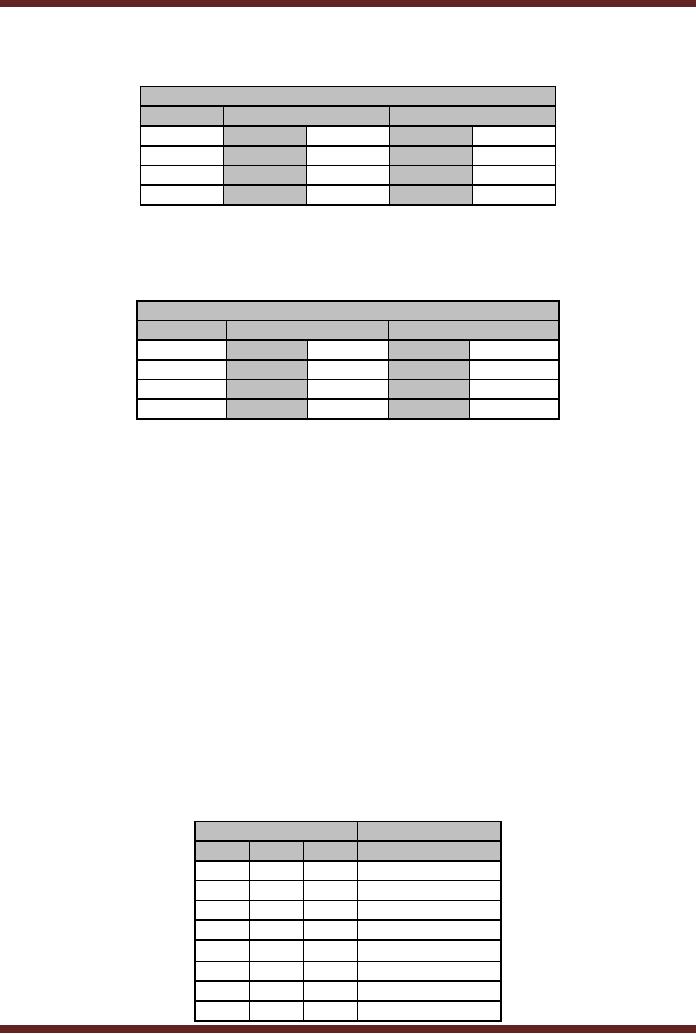
table specified. Table
15.1
Input
Output
Input
Output
S3
S2
S1
S0
F
S3
S2
S1
S0
F
0
0
0
0
0
1
0
0
0
0
0
0
0
1
0
1
0
0
1
0
0
0
1
0
0
1
0
1
0
1
0
0
1
1
0
1
0
1
1
1
0
1
0
0
0
1
1
0
0
1
0
1
0
1
0
1
1
0
1
1
0
1
1
0
0
1
1
1
0
1
0
1
1
1
0
1
1
1
1
1
Table
15.1
Function
Table of Invalid BCD Number
detector
S3S2\S1S0
00
01
11
10
00
0
0
0
0
0
0
01
0
0
11
1
1
1
1
10
0
0
1
1
Figure
15.2
Mapping of
Invalid BCD Number detector
function
The
Boolean expression for the
Invalid BCD Number Detector
obtained from the
Karnaugh Map
which maps the function
table is S
3S 2 + S 3S1 = S 3 (S 2 + S1 )
The
Invalid BCD Number is
represented by two error
conditions, either the BCD
number is one
of the
invalid numbers or a Carry
out has been generated.
Therefore the complete
expression
for
determining an incorrect BCD
output is Cout1 + S 3 (S 2 + S1 ) .
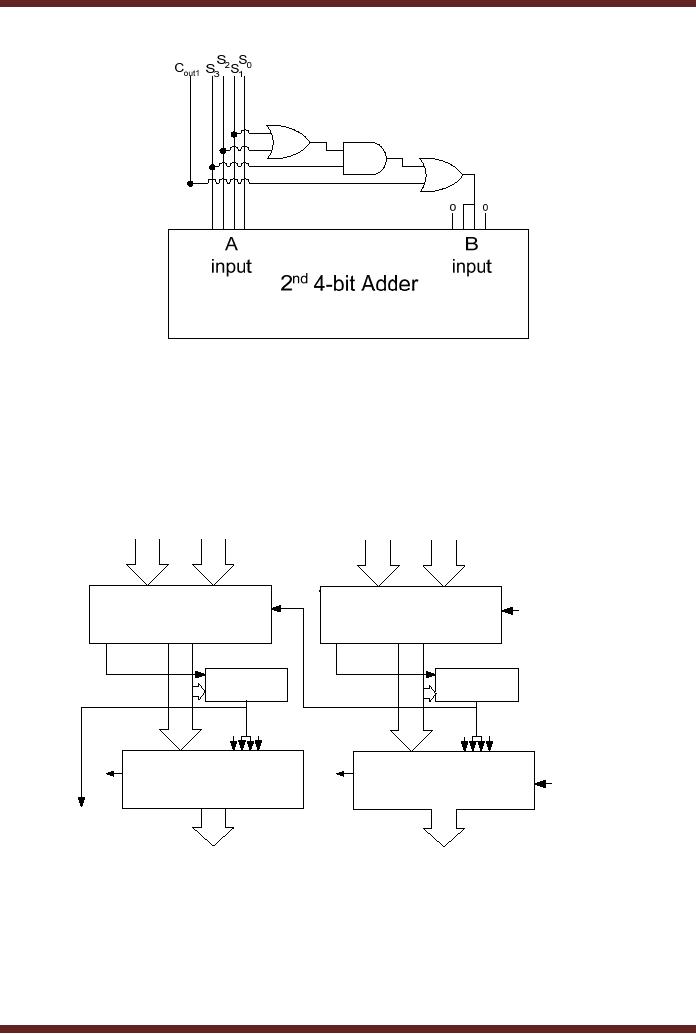
Figure 15.3
Figure
15.3
The
Invalid BCD Detector
Circuit
Connection of Invalid BCD Detector Circuit to second Adder
Adding of 6
when error conditions are
detected and adding a zero
when error
conditions
are not detected is
implemented by connecting the
output of the Invalid
BCD
Number
Detector circuit to bits B1 and B2
of the
Adder. Bits B0 and
B3 are
permanently
connected to 0.
Figure 15.4. When an error
condition is detected the
output of the circuit is
set
to logic 1,
setting bits B1 and
B2 to 1 and the
2nd Adder input B to
0110. When the
error
condition is
not detected the circuit
output is 0 and the 2nd Adder input B is set to
0000.
142
Figure
15.4
Using
the Second Adder to Add 6 or
0
2-digit BCD Adder
Two
singe digit BCD Adders
can be cascaded together to
form a 2-digit BCD
Adder.
Four,
4-bit 74LS283 MSI chips are
used. Two 74LS283s are
required to directly add the
two 2-
digit
BCD numbers and the
remaining two 74LS283s are
required to add a six to the
result if
any of
the two digits add up to
invalid BCD digits or
generate a Carry. Two
invalid BCD
detector
circuits are used. Figure
15.5
A4-7
B4-7
A0-3
B0-3
Cin4
Cin= 0
1st
1st
MSD 4-bit
Adder
LSD
4-bit Adder
Cout8
Cout4
Invalid
BCD
Invalid
BCD
Detector
Circuit
Detector
Circuit
S4-7
S0-3
0
0
0
0
Cin4=0
Cin= 0
Cout4
Cout8
2nd MSD 4-bit Adder
2nd LSD 4-bit
Adder
Cout
S4-7
S0-3
Figure
15.5
2-Digit
BCD Adder
Consider
two examples. In the first
example, 2-digit BCD number
99 is added with
another
2-digit BCD number 99.
The answer should be 198 a
3-digit BCD number. Table
15.2.
In the
second example, 2-digit BCD
number 99 is added with
another 2-digit BCD number
66.
The
answer should be 165. Table
15.3
143
1st MSD Adder
1st LSD Adder
Carry
A(0-3)
1001
A(0-3)
1001
B(0-3)
1001
B(0-3)
1001
Cin4
1
Cin
0
S(0-3)
0011
S(0-3)
0010
Cout8
1
Cout4
1
Ckt.
o/p 1
Ckt.
o/p 1
2nd LSD Adder
2nd LSD Adder
A(0-3)
0011
A(0-3)
0010
B(0-3)
0110
B(0-3)
0110
Cin
0
Cin
0
1
S(0-3)
1001
S(0-3)
1000
Table
15.2
Adding
BCD numbers 99 and 99
1st MSD Adder
1st LSD Adder
Carry
A(0-3)
1001
A(0-3)
1001
B(0-3)
0110
B(0-3)
0110
Cin4
1
Cin
0
S(0-3)
0000
S(0-3)
1111
Cout8
1
Cout4
0
Ckt.
o/p 1
Ckt.
o/p 1
2nd LSD Adder
2nd LSD Adder
A(0-3)
0000
A(0-3)
1111
B(0-3)
0110
B(0-3)
0110
Cin
0
Cin
0
1
S(0-3)
0110
S(0-3)
0101
Table
15.3
Adding
BCD numbers 99 and 66
Subtraction
Subtraction in
Digital Systems is performed by
taking the 2's complement of
the
number to be
subtracted (subtrahend) and
adding it to the minuend.
The example shows
the
subtraction of 6
represented in 2's complement
form from nine also
represented in its
2's
complement
form. Since 9 is a positive
number therefore its 2's
complement representation is
the
same. Neglecting the carry
bit, the 4-bit number
represents decimal 4.
9
1001
- 5
1011
4
1
0100
The
2's complement of any number
is obtained by taking the
1's complement of a
number
and then adding a 1 to the
1's complement. The two
step process to represent
a
negative
number in its 2's complement
form is shown
The
number 5
0101
144
Invert
all bits to result in 1's
complement
1's
complement of 5 is
1010
+1
2's
complement of 5 is
1011
An Adder
can be used to perform
subtraction operations if the
minuend is presented in
its
1's complemented form at the
input of the adder circuit.
The binary 1 that is added
to the 1's
complement of a
number to convert it into
2's complement is applied at
the Carry In of the
Adder
Circuit. Figure 15.6
1001
1010
A
(0-3)
B
(0-3)
Cout
Cin=1
4-bit
Parallel
Adder
Sum
(0-3)
Figure
15.6
4-bit
Subtraction Circuit
The
Adder circuit adds the
number 9 (1001), 1's
complement of 5 (1010) and
the Carry
In which is
set to 1.
A 4-bit bcd Adder/Subtracter Unit
An Adder
can be connected to perform
Additions and Subtractions by
applying the un-
complemented
and complemented data at one
of the two inputs of the
Adder respectively.
The
Carry In
input has also to be
connected to 0 or 1 respectively. Figure
15.7
B3
B2
B1
B0
Add =
0
Subtract =
1
U
C
U
C
U
C
U
C
A3 A2 A1 A0
CIn
COut
4-bit
Parallel Adder
S3 S2 S1 S0
Figure
25.7
4-bit
Adder/Subtracter Unit
145
The AND
gate and OR gate
implementation connected at the B
input of the 4-bit
Adder
is used to
allow Complemented or Un-Complemented B
input to be connected to the
Adder
input.
Adding of two 4-bit numbers
A and B can be performed by
selecting the Add/Subtract
=
0. The AND
gates marked U (un-complemented)
are enabled allowing B0-3 to be passed on
to
the OR
gates and the B input of
the Adder. Subtraction is
performed by selecting
the
Add/Subtract =
1. The AND gates marked C
(complemented) are enabled
allowing
complemented
B0-3 to be passed on to
the OR gates and the B
input of the Adder. The
Carry
In is also
set to 1 when Add/Subtract is
set to 1.
An 8-bit bcd Adder/Subtracter Unit
Two
4-bit 74LS283 chips can be
cascaded together to form an
8-bit Parallel Adder
Unit.
Each of the two 74LS283
ICs is connected to the 1's
Complement circuitry that
allows
either
the un-complemented form for
addition or the complemented
form for subtraction to
be
applied at
the B inputs of the two
74LS283s. Figure 15.8
The
8-bit Adder/Subtracter Circuit is
similar to the 4-bit
Adder/Subtracter Circuit.
Two
sets of
AND-OR based circuit that
allows complemented and
un-complemented B input to be
applied at
the B inputs of the two
4-bit Adders. The
Add/Subtract function select
input are tied
together.
The Carry In of the 1st 4-bit Adder circuit is
connected to the Add/Subtract
function
select
input. The Carry Out of
the 1st 4-bit Adder
circuit is connected to the
Carry In of the 2nd
4-bit
Adder circuit.
B7
B6
B5
B4
B3
B2
B1
B0
Add =
0
Subtract =
1
U
C
U
C
U
C
U
C
U
C
U
C
U
C
U
C
A7 A6 A5 A4
A3 A2 A1 A0
CIn
CIn
nd
1st 4-bit Parallel
Adder
2
4-bit
Parallel Adder
COut
S7 S6 S5 S4
S3 S2 S1 S0
Figure
15.8
8-bit
Adder/Subtracter Circuit
Consider
two number A=103 and
B=67 which are first
added and then subtracted
using the 8-
bit
Adder/Subtracter Circuit. Table
15.4 and Table
15.5
146
Adding
103 and 67
2nd MS Adder
1st LS Adder
Carry
A(4-7)
0110
A(0-3)
0111
B(4-7)
0100
B(0-3)
0011
Cin
0
Cin
0
0
S(4-7)
1010
S(0-3)
1010
Table
15.4
Adding
103 and 67
Subtracting
103 and 67
2nd MS Adder
1st LS Adder
Carry
A(4-7)
0110
A(0-3)
0111
B(4-7)
1011
B(0-3)
1100
Cin
1
Cin
1
1
S(4-7)
0010
S(0-3)
0100
Table
15.5
Subtracting
103 and 67
Arithmetic and Logic Unit (ALU)
Microprocessors
have Arithmetic and Logic
Units, a combinational circuit
that can
perform
any of the arithmetic
operations and logic
operations on two input
values. The
operation to be
performed is selected by set of
inputs known as function
select inputs.
There
are different MSI ALUs
available that have two
4-bit inputs a 4-bit output
and
three to
five function select inputs
that allows up to 32 different
functions to be performed.
Three
commercially available 4-bit
ALUS are
· 74XX181:
The 4-bit ALU has five
function select inputs
allowing it to perform 32
different
Arithmetic
and Logic operations.
· 74XX381:
The 4-bit ALU only has
three function select inputs
allowing only 8
different
arithmetic
and logic functions. Table
15.6
· 74XX382:
The 4-bit ALU is similar to
the 74XX381, the only
difference is that 74XX
381
provides
group-carry look-ahead outputs
and 74XX382 provides ripple
carry and overflow
outputs
Input
S2
S1
S0
Function
0
0
0
F=0000
0
0
1
F=B-A-1+Cin
0
1
0
F=A-B-1+Cin
0
1
1
F=A+B+Cin
F = A ⊕B
1
0
0
1
0
1
F=A+B
1
1
0
F=A.B
1
1
1
F=1111
147
Table
15.6
Function
Table of 74XX381 4-bit
ALU
Implementing 16-bit ALU
16-bit ALU
can be implemented by cascading
together four 4-bit ALUs.
These 4-bit
ALUs
have built in Look-Ahead
Carry Generator circuits
that eliminate the delay
caused by
carry
bit propagating through the
Parallel Adder circuit
within the 4-bit ALU circut.
However,
when a
number of such units are
cascaded together to implement
large 16-bit and 32-bit
ALU,
the
carry propagating between
one unit to the next
gets delayed due to the
Carry rippling
through
multiple 4-bit units. For
large 32-bit ALUs, the
Carry propagates through 8,
4-bit units
delaying
the Carry out from
the last most significant
unit by a factor of 8.The
74XX181 and
74XX381
circumvent the problem by
having Group-Carry
Look-Ahead.
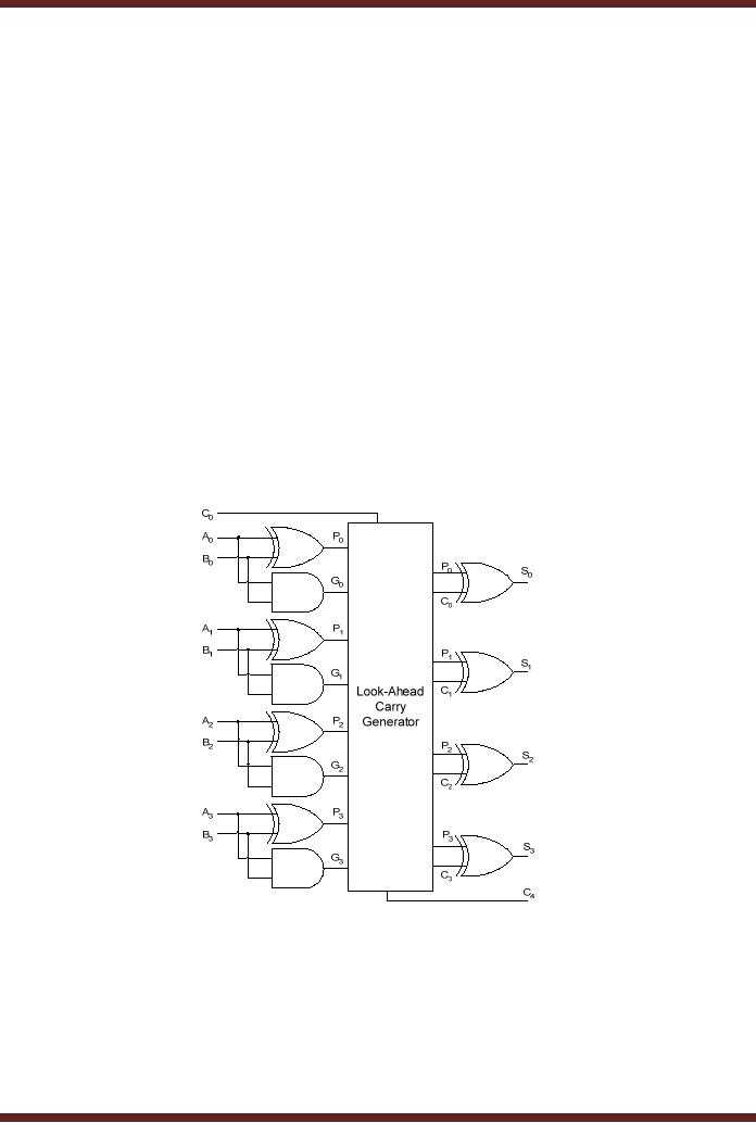
Group-Carry Look-Ahead
The
Look-Ahead Carry Generator
discussed earlier and used
by the 74LS283 Adder
provides
Carry's C1, C2, C3 and C4 simultaneously after a gate
delay of two. Carry's C1, C2 and
C3 are used internally,
where as C4
provides
the Cout from the 74LS283.
Referring to the
Look-
Ahead
Carry Generator Circuit the
C1, C2, C3 and C4
terms
are generated on the basis
of P0,
P1, P2 and P3 the four Carry
Propagate terms and G0, G1, G2 and
G3 the four
Carry Generate
terms.
Figure 15.9
Figure
15.9
Look-Ahead
Carry Generator
These
terms are used to generate
Group-Carry Look-Ahead outputs
that can be used
to cascade
together multiple units
eliminating the problem of
rippling carry. The G and
P
output
pins of the 74XX381 provide
the group-carry look-ahead
outputs that allow
multiple
ALUs to be
cascaded together. The
active-low outputs G and P
are represented by
the
Boolean
expressions. Figure
15.10
148
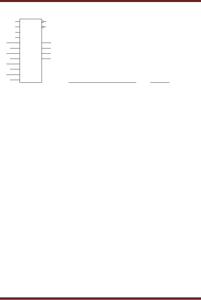
S0
S0
G
S1
S1
P
74X381
S2
S2
Cin
F4
A4
F0
A0
F5
B4
F1
B0
F6
A5
F2
A1
F7
B5
F3
B1
A6
A2
B6
B2
A7
A3
B7
B3
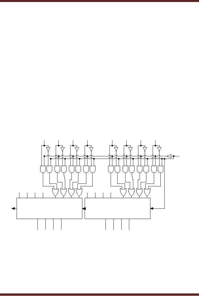
G = G3 + P3G 2 + P2P3G1 + P1P2P3G0
P = PoP1P2P3
Figure
15.10 74X381 ALU with
Group-Carry Look-Ahead
outputs
149