 |
CS302 -
Digital Logic & Design
Lesson
No. 19
DEMULTIPLEXER
A Multiplexer
has several inputs. It
selects one of the inputs
and routes the data at
the
selected
input to the single output.
Demultiplexer has an opposite
function to that of
the
Multiplexer. It
has a single input and
several outputs. The
Demultiplexer selects one of
the
several
outputs and routes the
data at the single input to
the selected output. A
demultiplexer
is also
known as a Data
Distributor.
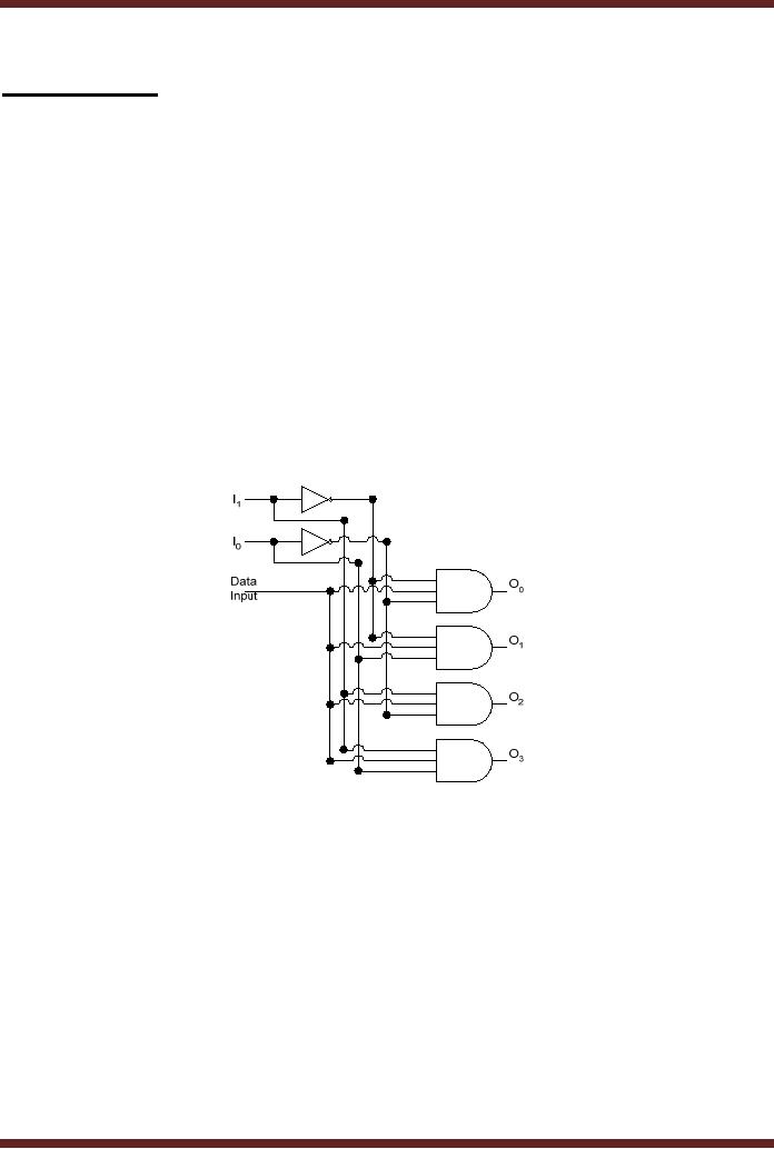
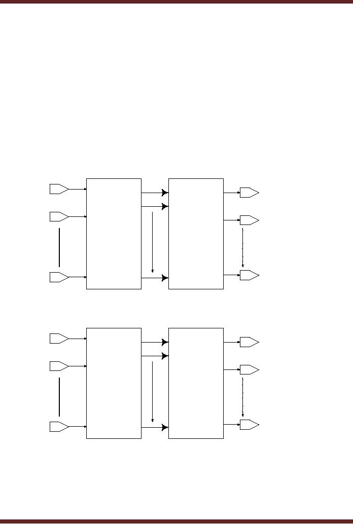
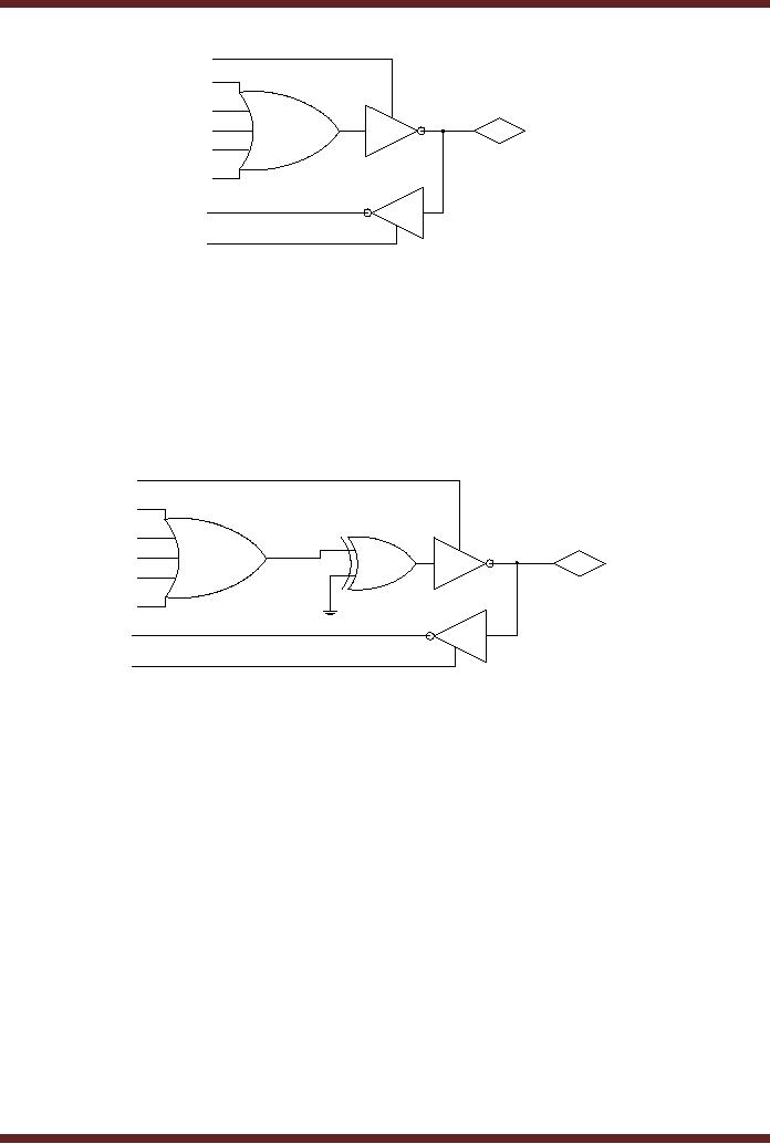
The
circuit diagram of a 1-to-4
line Demultiplexer is shown.
Figure 19.1. The circuit
if
compared to
that of the 2-to-4 Decoder.
The Decoder enable input is
used as the
Demultiplexer
data input. A Demultiplexer is
not available commercially. A
Demultiplexer is
available as a
Decoder/Demultiplexer chip which
can be configured to operate as
a
Demultiplexer or
a Decoder.
The
circuit of the 1-to-4
Demultiplexer is similar to the
2-to-4 Binary Decoder
described
earlier figure 16.9. The
only difference between the
two is the addition of the
Data
Input
line, which is used as
enable line in the 2-to-4
Decoder circuit figure
16.10. Assuming the
select
inputs I1
and I0 are set to 1 and 0
respectively. The O2 output is set to 1 if the
Data input
is 1 or it is
set to 0 if the Data input
is 0.
Figure
19.1
1-to-4
Demultiplexer
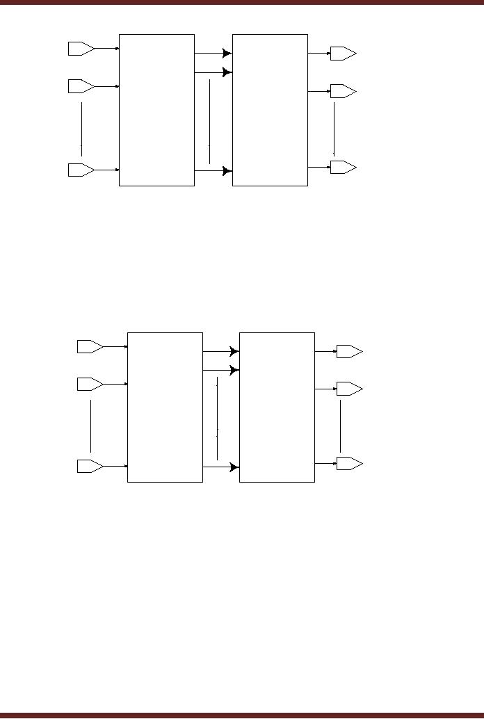
Applications of
Demultiplexer
Demultiplexer is
used to connect a single
source to multiple destinations.
One use of
the
Demultiplexer is at the output of
the ALU circuit. The output
of the ALU has to be stored
in
one of
the multiple registers or
storage units. The Data
input of the Demultiplexer is
connected
to the
output of the ALU. Each
output of the Demultiplexer is
connected to each of the
multiple
registers. By
selecting the appropriate
output data from the ALU is
routed to the
appropriate
register
for storage.
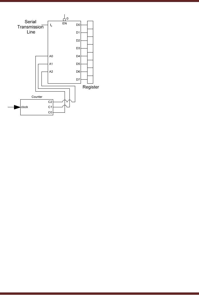
The
second use of the
Demultiplexer is the reconstruction of
Parallel Data from
the
incoming
serial data stream. Serial
data arrives at the Data
input of the Demultiplexer at
fixed
time
intervals. A counter attached to
the Select inputs of the
Demultiplexer routes the
incoming
serial
bits to successive outputs
where each bit is stored.
When all the bits
have been stored,
data
can be read out in parallel.
Figure 19.2
178
CS302 -
Digital Logic & Design
Figure
19.2
Demultiplexer as
a Serial to Parallel
Converter
Programmable
Logic Devices
Programmable
Logic Devices are used in
many applications to replace
the Logic gates
and MSI
chips. PLDs save circuit
space and reduce and
save the cost of components
in a
Digital
Circuit. PLDS consists of
Arrays of AND gates and OR
gates that can be
programmed
to perform
specific functions.
Programmable
Arrays of AND Gates and OR
Gates
The
array is essentially a grid of
conductors that forms rows
and columns with a
fuse
connecting
each column conductor with
each row conductor. The
fuses can be blown to
disconnect a
particular column from a
particular row. The OR gate
array consists of the
grid
and OR
gates. Similarly the AND
gate array consists of the
grid and AND Gates. Figure
19.3
Each
column conductor in the grid
represents a single variable or
its complement. A
grid of
several column conductors
represents several variables
and their complements.
Each
OR and AND
gate in the array is
connected to each of the
variables through
horizontal
conductors.
When all the fuses
are intact, all variables
are present at the inputs of
all the OR
and AND
gates. The OR and AND gates
can be configured to have
specified literals
connected to
their inputs by blowing away
appropriate fuses which are
blown through
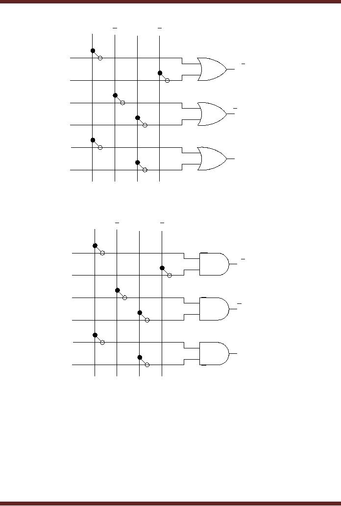
programming. A
programmed OR array has sum
terms at the output of its
OR gates. Similarly
a programmed AND
array has product terms at
its output. Figure
19.4
179
CS302 -
Digital Logic & Design
A
B
A
B
Fusible
Link
X1
X2
X3
Figure
19.3a OR Gate Array
A
B
A
B
Fusible
Link
X1
X2
X3
Figure
19.3b AND Gate Array
180
CS302 -
Digital Logic & Design
A
B
A
B
A +B
A +B
A +B
Figure
19.4a Programmed OR Gate
Array
A
B
A
B
AB
AB
AB
Figure
19.4b Programmed AND Gate
Array
An alternate
implementation of the grid is
with no fuses, the grid
column and row
conductors
are not connected to each
other. A specific column
conductor can be connected
to
a row
conductor by shorting the
column and row conductors.
Both the methods in which a
fuse
is blown to
disconnect a column from a
row and the shorting
method in which a column
is
connected to a
row can only be done
once. Thus when an array
has been configured
to
perform a
function it can not be
reprogrammed.
Programmable
Logic Devices have an array
of AND gates and an array of OR
gates
either or
both of which can be
programmed. There are
different types of PLDs,
they are
181
CS302 -
Digital Logic & Design
classified
according to their architecture
which allows either both
the arrays to be
programmed
or only
one of the two
arrays.
1. Programmable
Read-Only Memory
(PROM)
The
PROM consists of a fixed
non-programmable AND array configured as
a decoder
and a
programmable OR array. Figure
19.5. The PROM is used as a
storage device which
stores
information at addressable locations. It
has limited applications and
is not used as a
logic
device. PROM architecture
and details are discussed in
latter lectures.
2. Programmable
Logic Array (PLA)
The
PLA consists of a programmable AND
array and a programmable OR
array.
Figure
19.6. It has been designed
to overcome the limitations of a
PROM. PLA is also
known
as a
Field-Programmable Logic Array as it
can be programmed by the
user and not by
the
manufacturer.
`
Input
1
Output
1
Input
2
Output
2
Fixed
Programmable
AND
array
OR
array
Output
m
Input
n
Figure
19.5
Block
diagram of a PROM
`
Input
1
Output
1
Input
2
Output
2
Programmable
Programmable
AND
array
OR
array
Output
m
Input
n
Figure
19.6
Block
diagram of a PLA
3. Programmable
Array Logic (PAL)
The
PAL has been designed to
overcome the longer delays
and the complex
circuitry
associated
with the PLA due to two
programmable arrays. The PAL
has programmable AND
array
and a fixed OR array. Figure
19.7
182
CS302 -
Digital Logic & Design
`
Output
1
Input
1
Input
2
Output
2
Fixed
Programmable
AND
array
OR
array
and
output logic
Output
m
Input
n
Figure
19.7
Block
diagram of a PAL
4. Generic
Array Logic (GAL)
The GAL
has a reprogrammable AND array
and a fixed OR array with
programmable
output
logic. Figure 19.8. The
main difference between GAL
and PAL are the
reprogrammable
AND array
which can be programmed
again and again, unlike
PAL AND array which can
be
programmed
once. GAL uses E2CMOS
technology which is Electrically
Erasable CMOS
instead of
Bipolar technology and
fusible links. The other
difference is the
programmable
outputs.
`
Output
1
Input
1
Input
2
Output
2
Fixed
Programmable
AND
array
OR
array
and
Programmable
output
logic
Output
m
Input
n
Figure
19.8
Block
diagram of a GAL
All
the four PLD devices
use AND arrays followed by OR
arrays. Therefore they
all
allow
implementation of Sum-of-Product Boolean
expressions.
PAL Circuit
and Programming
A simplified
PAL structure is shown where
the AND array has been
programmed to
generate
three product terms which
are added together by the OR
array. Figure 19.9
183
CS302 -
Digital Logic & Design
A
B
A
B
AB
AB
AB + AB + AB
AB
Figure
19.9
PAL
programmed to implement an SOP
function
Input
Lines
Input
Buffers
B
A
B
A
A
Single
Line with slash
represents
multiple
AND gates inputs
B
X
X
2
X
X
X
2
X
X
2
Fuse
Intact
Fuse
Blown
(Connection)
(no
Connection)
Figure
19.10 Simplified diagram of
programmed PAL
PALs
have many inputs and
multiple outputs connected
through a large number
of
AND gates
and OR gates. Drawing the
circuit diagram of a PAL
having multiple gates
each
having
multiple inputs becomes
difficult. PALs have Buffers
at the inputs which produce
the
actual
variable and its complement.
The multiple input lines to
an AND gate array are
represented by a
single line with a slash
indicating the number of
inputs. The cross
indicates
184
CS302 -
Digital Logic & Design
the
fuses that are intact
showing a connection between
the vertical line and
horizontal line of
the AND
array. Figure 19.10
PAL
Outputs
PALs
typically have 8 or more
inputs to the AND array and
8 or less outputs from
the
fixed OR
array. Some PALs have
combined inputs and outputs
that can be programmed
as
either
inputs or outputs. PAL
output logic can be
configured according to the
application of the
PAL.
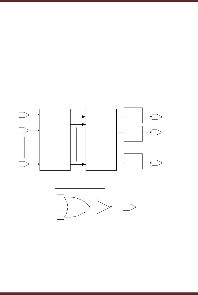
The modified block diagram
representing a PAL showing
the output of the OR
Array
connected to
output logic which allows
the outputs to be configured is
shown in figure
19.11.
The
three types of outputs
are
· Combinational
Output used for an SOP
function and is available as an
active-high or
active-low
output. Figure 19.12a
· Combinational
Input/Output is used when
the output is connected back
to the input of the
PAL or if
the output pin is used as an
input only. Figure
19.12b
· Programmable
polarity output is used to
either select the output
function or its
complement
by programming
an XOR gate at the output.
Figure 19.12c
Output
`
Input
1
Output
1
Logic
Output
Input
2
Output
2
Fixed
Programmable
Logic
AND
array
OR
array
Output
Output
m
Logic
Input
n
Figure
19.11 Block diagram of a PAL
with programmable
outputs
From
AND
Output
gate
array
Figure
19.12a Combinational Output
with active-low
output
The
output of the OR gate from
the OR gate Array is shown
to be connected to a tri-
state
buffer input. The tri-state
buffer can be activated or
deactivated through the
control line
shown
connected to its side. The
Combinational Output for an
SOP function is implemented
by
activating
the tri-state buffer which
allows the output of the OR
gate to be inverted by the
tri-
state
buffer and passed to the
output of the PAL device. An
active-high output can be
obtained
if the
PAL device has active-high
output tri-state
buffers.
185
CS302 -
Digital Logic & Design
From
AND
Input
/
gate
array
Output
Figure
19.12b Combinational Input/Output
with active-low
output
The
Combinational input/output function is
used when the output of
the OR gate has to
be connected
back to the input of the AND
Gate. As shown in the figure
the output of the
tri-
state
buffer is connected to the
input of an inverting and
non-inverting buffer which
allows the
inverted
and non-inverted outputs of
the OR gate to be connected to
the input of the AND
gate
array.
Secondly, by deactivating the
tri-state buffer connected at
the output of the OR
Gate,
the
output pin is configured as an
input pin. External signals
connected to the output pin
are
passed to
the input of the AND
array.
Input
/
From
AND
Output
X
gate
array
Figure
19.12c Programmed Polarity
output
The
Programmed Polarity output
has the output of the OR
gate connected through
an
XOR
gate to the tri-state
buffer. The XOR gate
allows the output of the OR
gate to be set to
active-high or
active-low. When the second
input of the XOR gate is
connected to ground,
the
output of
the XOR gate is the
same as the output of the OR
gate. When the fuse of
the XOR
gate
input is blown to set the
input to logic high, the
output of the XOR gate is
opposite of the
OR gate
output.
PAL
Identification
PALs
come in different configurations
they are identified by
unique number. The
numbers
begin with the prefix
PAL followed by two digits
that indicate the number of
inputs
followed by a
letter L active-low, H active-high or P
programmable polarity followed by a
single
or two
digits that indicate the
number of outputs. In addition to
the standard number there
may
be suffixes
which specify the speed,
package type and temperature
range. Figure 19.13
186
CS302 -
Digital Logic & Design
P A L 10 L
8
Programmable
array Logic
Eight
Outputs
Active
Low output
Ten
Inputs
Figure
19.13 Standard PAL
Numbering
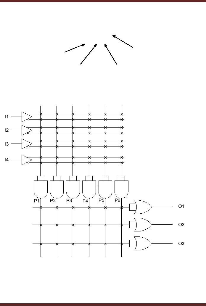
PLA Circuit
and Programming
Figure
19.14 A 4 x 3 PLA
Device
Programmable
Logic Array as mentioned
earlier has a programmable AND
and OR
arrays. A
PLA can be programmed to
implement any Sum-of-Product
logic expressions,
limited by
the parameters of the PLA
device. The limitations
are
· Number of
inputs (n)
· Number of
outputs (m)
187

CS302 -
Digital Logic & Design
·
Number of
product terms (p)
Such a
device is described as an n x m PLA
device with p product terms.
The simplified
diagram of a
PLA 4 x 3 device is shown in
the figure 19.14. The
four inputs I1, I2, I3
and I4 are
shown
connected through input
buffers to the input of the
AND gate array. The Input
buffers
provide
the un-complemented and
complemented input signals.
Each of the 6 AND
gates
which
provide six product terms
P1, P2, P3, P4 P5 and P6
have 8 inputs. The outputs
of each
of the
six AND gates are connected
to the input of the OR gate
array. Each of the three
OR
gates
six inputs. Each OR gate
can thus perform a sum
operation on six product
terms.
The
PLA allows both its AND
Gate array and the OR
gate array to be
programmed
independently.
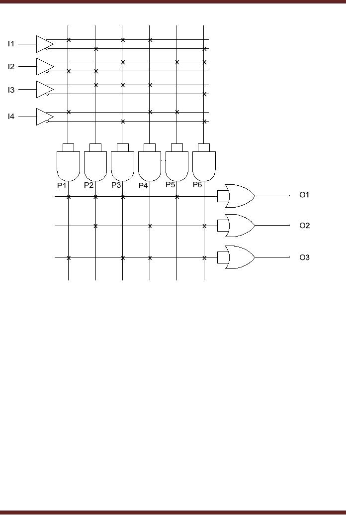
The 4 x 3 PLA programmed
with three separate
functions is show in
figure
19.15.
The product terms generated
are
P1 = I1.I2.I4
P2 = I1.I2.I3
P3 = I1.I2.I3.I4
P4 = I1.I3.I4
P5 = I2.I4
P6 = I1.I2.I3.I4
The
first OR gate sums product
terms P1, P2, P3 and
P5, the fuses for
these product terms
are
seen to be intact. The
second OR gate sums the
product terms P2, P4 and
P6. The third
OR gate
sums the product terms
P1, P3, P4 and P6.
The three sum-of-product
terms are
O1 = I1.I2.I4 + I1.I2.I3 + I1.I2.I3.I4 + I2.I4
O2 = I1.I2.I3 + I1.I3.I4 + I1.I2.I3.I4
O3 = I1.I2.I4 + I1.I2.I3.I4 + I1.I3.I4 + I1.I2.I3.I4
188
CS302 -
Digital Logic & Design
Figure
19.15 Programmed 4 x 3 PLA
Device
189
Table of Contents:
- AN OVERVIEW & NUMBER SYSTEMS
- Binary to Decimal to Binary conversion, Binary Arithmetic, 1s & 2s complement
- Range of Numbers and Overflow, Floating-Point, Hexadecimal Numbers
- Octal Numbers, Octal to Binary Decimal to Octal Conversion
- LOGIC GATES: AND Gate, OR Gate, NOT Gate, NAND Gate
- AND OR NAND XOR XNOR Gate Implementation and Applications
- DC Supply Voltage, TTL Logic Levels, Noise Margin, Power Dissipation
- Boolean Addition, Multiplication, Commutative Law, Associative Law, Distributive Law, Demorgans Theorems
- Simplification of Boolean Expression, Standard POS form, Minterms and Maxterms
- KARNAUGH MAP, Mapping a non-standard SOP Expression
- Converting between POS and SOP using the K-map
- COMPARATOR: Quine-McCluskey Simplification Method
- ODD-PRIME NUMBER DETECTOR, Combinational Circuit Implementation
- IMPLEMENTATION OF AN ODD-PARITY GENERATOR CIRCUIT
- BCD ADDER: 2-digit BCD Adder, A 4-bit Adder Subtracter Unit
- 16-BIT ALU, MSI 4-bit Comparator, Decoders
- BCD to 7-Segment Decoder, Decimal-to-BCD Encoder
- 2-INPUT 4-BIT MULTIPLEXER, 8, 16-Input Multiplexer, Logic Function Generator
- Applications of Demultiplexer, PROM, PLA, PAL, GAL
- OLMC Combinational Mode, Tri-State Buffers, The GAL16V8, Introduction to ABEL
- OLMC for GAL16V8, Tri-state Buffer and OLMC output pin
- Implementation of Quad MUX, Latches and Flip-Flops
- APPLICATION OF S-R LATCH, Edge-Triggered D Flip-Flop, J-K Flip-flop
- Data Storage using D-flip-flop, Synchronizing Asynchronous inputs using D flip-flop
- Dual Positive-Edge triggered D flip-flop, J-K flip-flop, Master-Slave Flip-Flops
- THE 555 TIMER: Race Conditions, Asynchronous, Ripple Counters
- Down Counter with truncated sequence, 4-bit Synchronous Decade Counter
- Mod-n Synchronous Counter, Cascading Counters, Up-Down Counter
- Integrated Circuit Up Down Decade Counter Design and Applications
- DIGITAL CLOCK: Clocked Synchronous State Machines
- NEXT-STATE TABLE: Flip-flop Transition Table, Karnaugh Maps
- D FLIP-FLOP BASED IMPLEMENTATION
- Moore Machine State Diagram, Mealy Machine State Diagram, Karnaugh Maps
- SHIFT REGISTERS: Serial In/Shift Left,Right/Serial Out Operation
- APPLICATIONS OF SHIFT REGISTERS: Serial-to-Parallel Converter
- Elevator Control System: Elevator State Diagram, State Table, Input and Output Signals, Input Latches
- Traffic Signal Control System: Switching of Traffic Lights, Inputs and Outputs, State Machine
- Traffic Signal Control System: EQUATION DEFINITION
- Memory Organization, Capacity, Density, Signals and Basic Operations, Read, Write, Address, data Signals
- Memory Read, Write Cycle, Synchronous Burst SRAM, Dynamic RAM
- Burst, Distributed Refresh, Types of DRAMs, ROM Read-Only Memory, Mask ROM
- First In-First Out (FIFO) Memory
- LAST IN-FIRST OUT (LIFO) MEMORY
- THE LOGIC BLOCK: Analogue to Digital Conversion, Logic Element, Look-Up Table
- SUCCESSIVE APPROXIMATION ANALOGUE TO DIGITAL CONVERTER