 |
CS302 -
Digital Logic & Design
Lesson
No. 23
APPLICATION OF
S-R LATCH
Digital
systems use switches to
input values and to control
the output. For example,
a
keypad
uses 10 switches to enter
decimal numbers 0 to 9. When a
switch is closed the
switch
contacts
physically vibrate or `bounce'
before making a solid
contact. The switch
bounce
causes
the voltage at the output of
the switch to vary between
logic low and high
for a very
short
duration before it settles to a
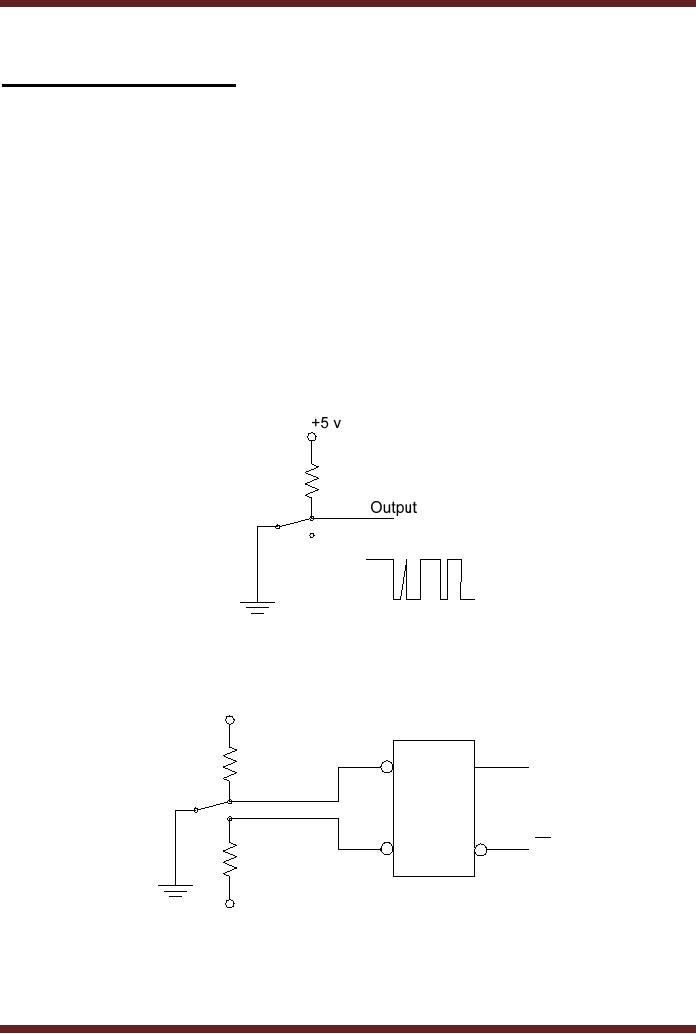
steady state. Figure 23.1a.
The variation in the
voltage
causes
the digital circuit to
operate in an erratic manner. An
S-R latch connected between
the
switch
and the digital circuit
prevents the varying switch
output from reaching the
digital circuit.
Figure
23.1b.
In the
figure 23.1a when the
switch is moved up to connect
the resistor to the
ground,
the
output voltage fluctuates
between logic 1 and 0 for a
very brief period of time
when the
switch
vibrates before making a
solid contact. The output
voltage settles to logic 0
when a
solid
contact is made. The
active-low input S-R latch
shown in figure 23.1b
prevents the output
signal
from varying between logic 1
and 0. When the switch is
moved from down position to
up
position,
the R input is set to 1 and
S input is set to 0, which
sets the Q output of the
S-R latch
to 1. The S
input varies between 0 and 1
due to switch `bounce',
however the S-R
latch
doesn't
change its output state Q
when S = 1 and R = 1.
Figure
23.1a The output of a switch
connected to Logic
High
+5 v
Output
S
Q
Active-low
Input
S-R
Latch
R
Q
+5 v
Figure
23.1b The switch connected
through an S-R latch
224
CS302 -
Digital Logic & Design
S
Q
R
Q
Figure
23.1c The switch connected
through an S-R latch
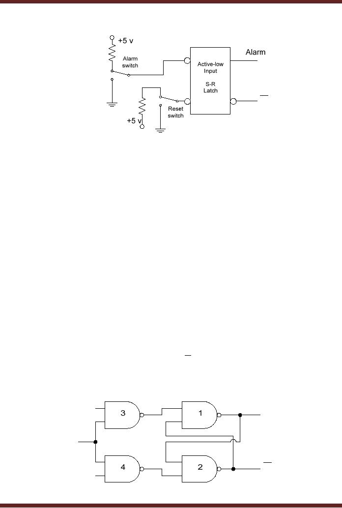
The
circuit diagram in figure
23.1c shows a burglar alarm
circuit. The alarm switch
is
connected to
logic high connecting the S
input to logic high. The
alarm is activated by
setting
the
reset switch to ground
connecting the R input to 0
volts. This sets the Q
output of the latch
to 0. The
switch is reset to logic
high. When an intruder opens
a door the alarm switch
is
connected to
ground or logic 0. The set
input is set to logic 0,
setting the Q output to
logic 1
and
activating the alarm. If the
door is closed the alarm
switch is reconnected to logic
1,
however
the Q output is maintained at
logic 1 and the alarm
continues to sound as S=1
and
R=1
which maintains the output.
The alarm can only be
disabled by reconnecting the
reset
switch to
ground.
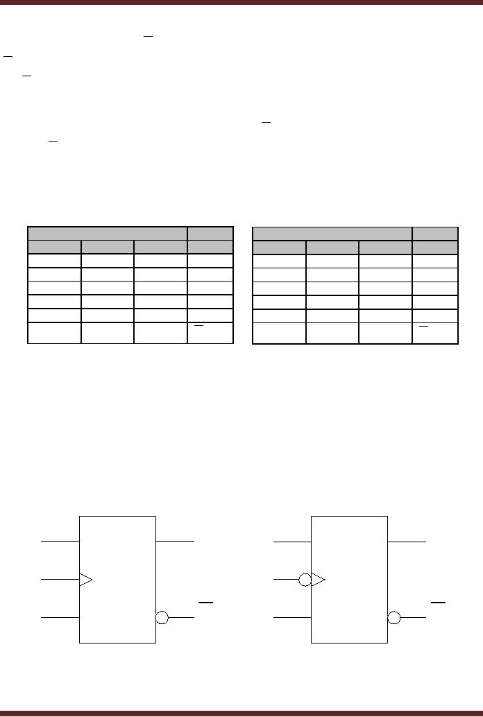
The
S-R NAND gate based latch is
available in the form of an
Integrated Circuit.
The
74LS279 IC
has four S-R latches
which can be used
independently.
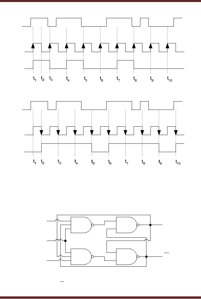
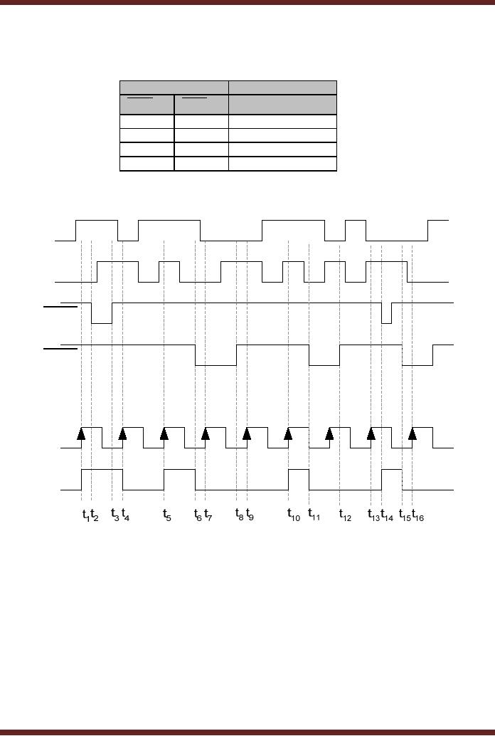
The
Gated S-R Latch
The
gated S-R latch has an
enable input which has to be
activated to operate the
latch.
The
circuit diagram of the gated
S-R latch is shown. Figure
23.2. In the gated S-R
circuit, the S
and R
inputs are applied at the
inputs of the NAND gates 1
and 2 when the enable
input is set
to active-high.
If the enable input is
disabled by setting it to logic
low the output of NAND
gates
3 and 4
remains logic 1, what ever
the state of S and R inputs.
Thus logic 1 applied at
the
inputs of NAND
gates 1 and 2 keeps the Q
and Q outputs to
the previous state. The
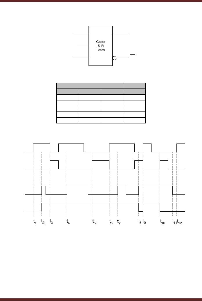
logic
symbol of a
gated S-R latch is shown in
figure 23.3. The Truth
Table of the gated S-R
latch is
shown in
table 23.1. The timing
diagram showing the
operation of the gated S-R
latch is
shown in
figure 23.4
S
Q
EN
Q
R
Figure
23.2
Gated
S-R Latch
225
CS302 -
Digital Logic & Design
S
Q
EN
R
Q
Figure
23.3
Logic
Symbol of a Gated S-R
Latch
Input
Output
EN
S
R
Qt+1
0
x
x
Qt
1
0
0
Qt
1
0
1
0
1
1
0
1
1
1
1
invalid
Table
23.1
Truth-Table of a
gated S-R Latch
S
R
EN
Q
Figure
23.4
Timing
diagram of a gated S-R
latch
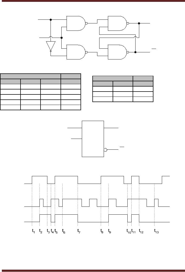
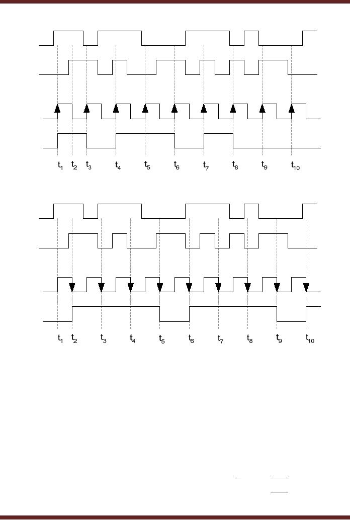
The
Gated D Latch
If the S
and R inputs of the gated
S-R latch are connected
together using a NOT
gate
then
there is only a single input
to the latch. The input is
represented by D instead of S or
R.
Figure
23.5. The gated D-latch
can either have D set to 0
or 1, thus the four
input
combinations
applied at the S-R inputs of
an S-R latch reduce to only
two input
combinations.
Table
23.2. The logic symbol of a
gated D-latch is shown in
figure 23.6. The timing
diagram of
the
operation of a D-latch is shown in
figure 23.7. The Q output of
the D latch is seen to
be
following
the D input.
226
CS302 -
Digital Logic & Design
D
Q
3
1
EN
Q
4
2
Figure
23.5
Gated D
Latch
Input
Output
Input
Output
EN
S
(D)
R
Qt+1
EN
D
Qt+1
0
x
X
Qt
0
x
Qt
1
0
0
Qt
1
0
0
1
0
1
0
1
1
1
1
1
0
1
1
1
1
Invalid
Table
23.2
Truth-Table of a
gated D Latch
D
Q
Gated
EN
D
Latch
Q
Figure
23.6
Logic
Symbol of a Gated D
Latch
D
EN
Q
Figure
23.7
Timing
diagram of a gated D
latch
Application of
Gated D Latch
The D
latch is available in the
form of an Integrated Circuit.
The 74LS75 has four
D
latches
which can be used
independently. The gated D
latch can be used to store
binary
information.
The circuit shown in figure
23.8 uses the gated
D-latches connected at the
input
227
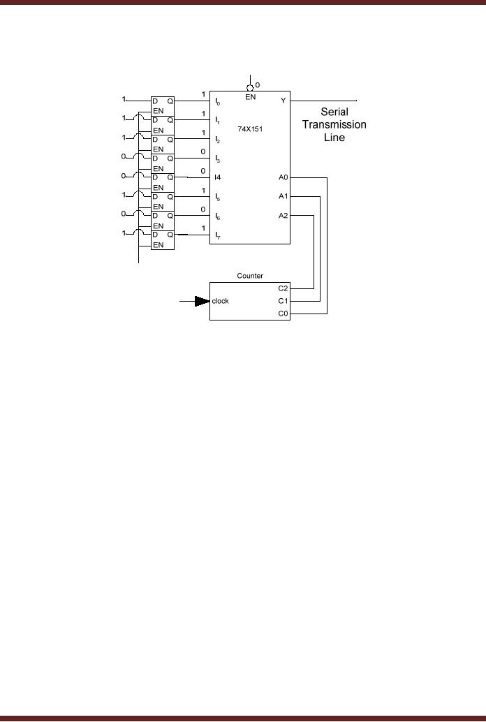
CS302 -
Digital Logic & Design
of 1-of-8
multiplexer to store a byte
value (parallel). The
multiplexer accesses each
bit value
stored in
the D-latch and routes it to
the output. Thus the
8-bit (byte) parallel data
is converted
into
serial data.
Figure
23.8
Gated
D-latch used to store
parallel data
Edge-Triggered
Flip-Flop
Flip-Flops
are synchronous bi-stable
devices, known as bi-stable
multivibrators. Flip-
flops
have a clock input instead
of a simple enable input as
discussed earlier. The
output of
the
flip-flop can only change
when appropriate inputs are
applied at the S and R
inputs and a
clock
signal is applied at the
clock input. Flip-flops with
enable inputs can change
their state at
any
instant when the enable
input is active. Digital
circuits that change their
outputs when the
enable
input is active are
difficult to design and
debug as different parts of
the digital circuit
operate at
different times.
In Synchronous
systems, the output of all
the digital circuits changes
when a clock
signal is
applied instead of the
enable signal. The change in
the state of the digital
circuit
occurs
either at the low-to-high or
high-to-low transition of the
clock signal. Since the
transition
of the
clock signal is for a very
short a precise time
intervals thus all digital
parts of a Digital
system
change their states
simultaneously. The low to
high or high to low
transition of the
clock is
considered to be an edge. Three
different types of edge-triggered
flip-flops are
generally
used in digital logic
circuits.
·
S-R
edge-triggered flip-flop
·
D edge-triggered
flip-flop
·
J-K
edge-triggered flip-flop
Each
flip-flop has two
variations, that is, it is
either positive edge-triggered or
negative edge
triggered. A
positive edge-triggered flip-flop
changes its state on a
low-to-high transition of
the
clock
and a negative edge-triggered
flip-flop changes its state
on a high-to-low transition of
the
clock.
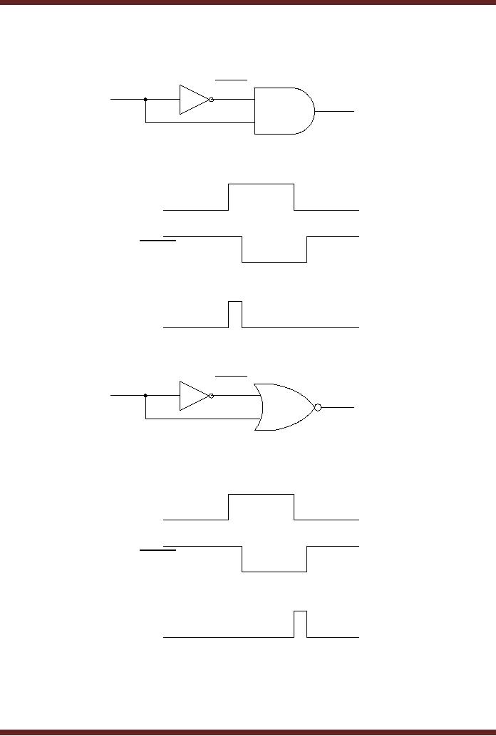
The edge-detection circuit
which allows a flip-flop to
change its state on either
the
positive or
the negative transition of
the clock is implemented
using a simple
combinational
228
CS302 -
Digital Logic & Design
circuit.
The edge detection circuit
that detects the positive
and the negative clock
transition are
shown in
figure 23.9.
CLK
CLK
CLK PULSE
Figure
23.9a Positive clock edge
detection circuit
CLK
CLK
CLK PULSE
Figure
23.9b Timing diagram of the
Positive clock edge
detection circuit
CLK
CLK
CLK PULSE
Figure
23.9c Negative clock edge
detection circuit
CLK
CLK
CLK PULSE
Figure
23.9d Timing diagram of the
Negative clock edge
detection circuit
Edge-Triggered
S-R Flip-flop
229
CS302 -
Digital Logic & Design
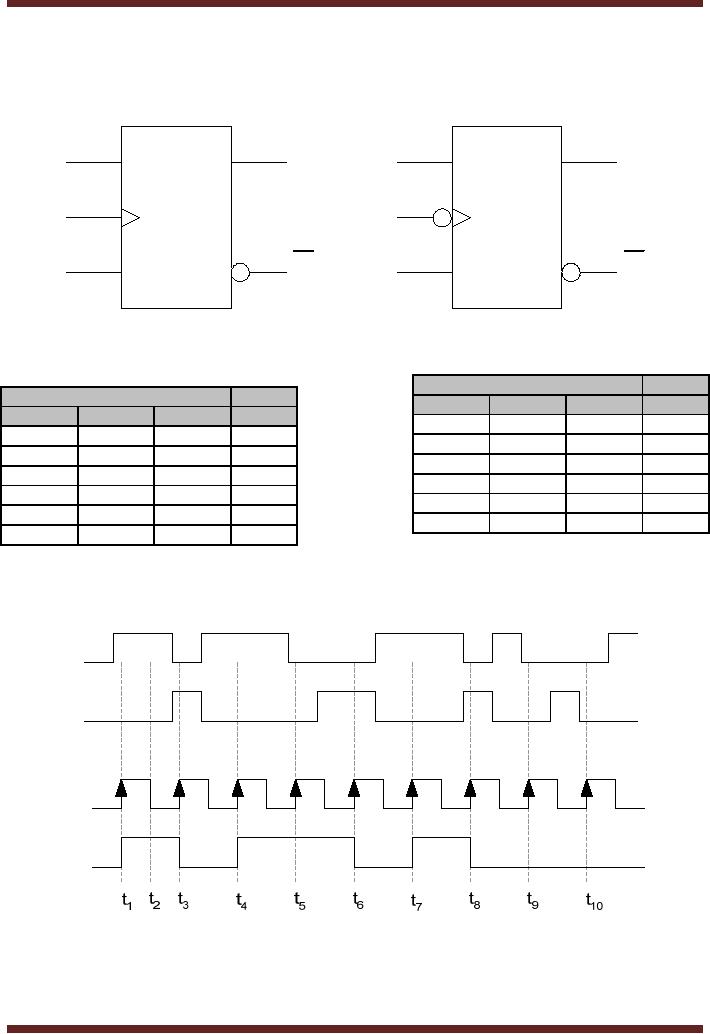
The
Logic symbols of a positive
edge and a negative edge
triggered S-R flip-flops
are
shown in
figure 23.10. The truth
table of the two S-R
flip-flops are shown. Table
23.3. The
timing
diagrams of the two S-R
flip-flops are shown in
figure 23.11.
S
S
Q
Q
S-R
S-R
CLK
CLK
Flip-Flop
Flip-Flop
R
R
Q
Q
Figure
23.10 Logic Symbol of
Positive and Negative edge
triggered S-R
flip-flops
Input
Output
Input
Output
CLK
S
R
Qt+1
CLK
S
R
Qt+1
0
x
x
Qt
0
X
X
Qt
1
x
x
Qt
1
X
X
Qt
↓
0
0
Qt
↑
0
0
Qt
↓
0
1
0
↑
0
1
0
↓
1
0
1
↑
1
0
1
↓
1
1
invalid
↑
1
1
invalid
Table
23.3
Truth-Table of
Positive and Negative Edge
triggered S-R
flip-flops
S
R
CLK
Q
Figure
23.11a Timing diagram of a
Positive Edge triggered S-R
flip-flop
230
CS302 -
Digital Logic & Design
S
R
CLK
Q
Figure
23.11b Timing diagram of a
Negative Edge triggered S-R
flip-flop
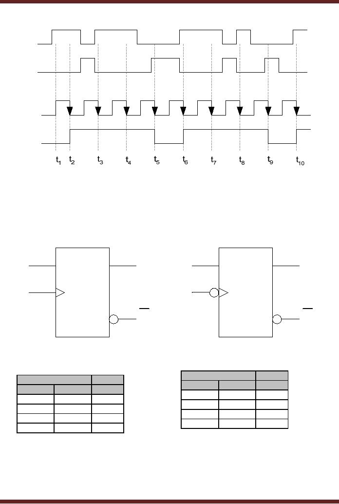
Edge-Triggered D
Flip-flop
The
Logic symbols of a positive
edge and a negative edge
triggered D flip-flops
are
shown in
figure 23.12. The truth
table of the two D
flip-flops are shown. Table
23.4. The timing
diagrams of
the two D flip-flops are
shown in figure
23.13.
Q
Q
D
D
D
D
CLK
CLK
Flip-Flop
Flip-Flop
Q
Q
Figure
23.12 Logic Symbol of
Positive and Negative edge
triggered D flip-flops
Input
Output
Input
Output
CLK
D
Qt+1
CLK
D
Qt+1
0
X
Qt
0
X
Qt
1
X
Qt
1
X
Qt
↓
0
0
↑
0
0
↓
1
1
↑
1
1
Table
23.4
Truth-Table of
Positive and Negative Edge
triggered D flip-flops
231
CS302 -
Digital Logic & Design
D
CLK
Q
Figure
23.13a Timing diagram of a
Positive Edge triggered D
flip-flop
D
CLK
Q
Figure
23.13b Timing diagram of a
Negative Edge triggered D
flip-flop
Edge-Triggered
J-K Flip-flop
The
J-K flip-flop is widely used
in digital circuits. Its
operation is similar to that of
the S-
R flip-flop
except that the J-K
flip-flop doesn't have an
invalid state, instead it
toggles its state.
The
circuit diagram of a J-K
edge-triggered flip-flop is shown in
figure 23.14
J
Q
3
1
CLK
Q
4
2
K
Figure
23.14 Edge-triggered J-K
flip-flop
Consider
the Q and Q output of
the J-K flip-flop set to 1
and 0 respectively and 0 and
1
respectively.
Four set of inputs are
applied at J and K, the
effect on the outputs is as
follows.
232

CS302 -
Digital Logic & Design
J = 0 and K
=0
With
Q=1 and Q =0, on a
clock transition the outputs
of NAND gates 3 and 4 are
set to
logic 1.
With logic 1 value at the
inputs of NAND gates 1 and 2
the output Q and Q remains
unchanged.
With Q=0 and Q =1, on a
clock transition the outputs
of the NAND gates 3 and
4
are
set to logic 1. With logic 1
value at the inputs of NAND
gates 1 and 2 the output Q
and Q
remains
unchanged.
Thus
when J=0 and K=0
the previous state is
maintained and there is no
change in the
output.
J = 0 and K
=1
With
Q=1 and Q =0, on a
clock transition the output
of NAND gate 3 is set to logic
1.
The
output of the NAND gate 4 is
set to 0 as all three of its
inputs are at logic 1. The
logic 1
and 0 at
the inputs of the NAND gates
3 and 4 respectively resets
the Q output to 0 and Q to
1. With
Q=0 and Q =1, on a
clock transition the output
of NAND gate 3 is set to logic 1.
The
output of
the NAND gate 4 is also set
to 1 as the input of the NAND
gate 4 is connected to
Q=0.
The logic 1 and 1 at the
inputs of the NAND gates 3
and 4 respectively retains
the Q and
Q to 0 and 1
respectively.
Thus
when J=0 and K=1
the J-K flip-flop
irrespective of its earlier
state is rest to
state
Q=0
and Q =1.
J = 1 and K
=0
With
Q=1 and Q =0, on a
clock transition the output
of NAND gate 4 is set to logic
1.
The
output of the NAND gate 3 is
also set to 1 as its input
connected to Q is at logic 0.
Thus
inputs 1
and 1 at inputs of NAND gates 1
and 2 retain the Q and
Q output to 1
and 0
respectively.
With Q=0 and Q =1, on a
clock transition the output
of NAND gate 4 is set to
logic 1.
The output of the NAND gate
3 is set to 0 as all its
input are at logic 1. Thus
inputs 0
and 1 at
inputs of NAND gates 1 and 2
sets the flip-flop to Q=1
and Q =0.
Thus
when J=1 and K=0
the J-K flip-flop
irrespective of its output
state is set to state
Q=1
and Q =0.
J = 1 and K
=1
With
Q=1 and Q =0, on a
clock transition the output
of the NAND gates 3 and 4
depend
on the
outputs Q and Q . The
output of NAND gate 3 is set to 1 as
Q is connected to
its input.
The
output of NAND gate 4 is set to 0 as
all its inputs including Q
is at logic 1. A logic 1 and
0
at the
input of gates 1 and 2
toggles the outputs Q and
Q from
logic 1 and 0 to 0 and
1
233
CS302 -
Digital Logic & Design
respectively.
With Q=0 and Q =1, on a
clock transition the output
of NAND gate 3 is set to 0 as
Q and
the output of NAND gate 4 is
set to 1. A logic 0 and 1 at
the input toggles the
outputs Q
and Q from
logic 0 and 1 to 1 and 0
respectively.
In summary
when J-K inputs are
both set to logic 0, the
output remains unchanged.
At
J=0
and K=1 the J-K
flip-flop is reset to Q=0
and Q =1. At
J=1 and K=0 the
flip-flop is set to
Q=1
and Q =0.
With J=1 and K=1
the output toggles from
the previous state. The
truth tables
of the
positive and negative edge
triggered J-K flip-flops are
shown in table 23.5. The
logic
symbols of
the J-K flip-flops are
shown in figure 23.15. The
timing diagrams of the J-K
flip-
flops
are shown in figure
23.16.
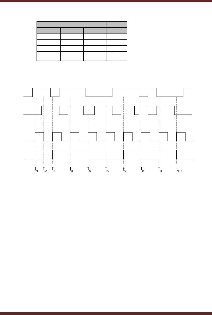
Input
Output
Input
Output
CLK
J
K
Qt+1
CLK
J
K
Qt+1
0
x
X
Qt
0
x
x
Qt
1
x
X
Qt
1
x
x
Qt
↑
0
0
Qt
↓
0
0
Qt
↑
0
1
0
↓
0
1
0
↑
1
0
1
↓
1
0
1
↑
1
1
↓
1
1
Qt
Qt
Table
23.5
Truth-Table of
Positive and Negative Edge
triggered J-K
flip-flops
J
J
Q
Q
J-K
J-K
CLK
CLK
Flip-Flop
Flip-Flop
K
K
Q
Q
Figure
23.15 Logic Symbol of
Positive and Negative edge
triggered J-K
flip-flops
234
CS302 -
Digital Logic & Design
J
K
CLK
Q
Figure
23.16a Timing diagram of a
Positive Edge triggered J-K
flip-flop
J
K
CLK
Q
Figure
23.16b Timing diagram of a
Negative Edge triggered J-K
flip-flop
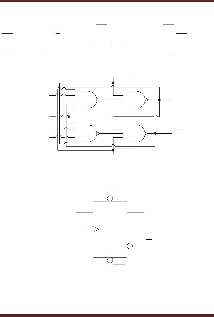
Asynchronous
Preset and Clear
Inputs
The
S-R, J-K and D inputs
are known as synchronous
inputs because the
outputs
change
when appropriate input
values are applied at the
inputs and a clock signal is
applied at
the
clock input. If there is no
clock transition then the
inputs have no effect on the
output.
Digital
circuits require that the
flip-flops be set or reset to
some initial state before a
new set of
inputs is
applied for changing the
output. The flip-flops are
set-reset to some initial
state by
using
asynchronous inputs known as
Preset and Clear inputs.
Since these inputs change
the
output to a
known logic level
independently of the clock
signal therefore these
inputs are
known as
asynchronous inputs. The
circuit diagram of a J-K
flip-flop with Preset and
Set
Asynchronous
inputs is shown in figure
23.17. The asynchronous
inputs override the
synchronous
inputs thus to operate the
flip-flop in the synchronous
mode the asynchronous
inputs
have to be disabled. To preset
the flip-flop to Q=1 and
Q =0 the
PRE input is set to
0
which
sets the Q output to 1 and
the output of NAND gate 4 to 1.
The CLR input is set to 1
235
CS302 -
Digital Logic & Design
which
sets the Q output to 0 as
all three inputs of the NAND
gate 2 are set to 1. The
flip-flop
is cleared to
Q=0 and Q =1 by setting
the PRE input is set to 1 and
the CLR input is to 0. The
CLR input set to 0
sets Q =1 it also
sets the output of NAND gate
3 to 1. The PRE input set to
1 sets
the output Q to 0. When the
PRE and the
CLR inputs are
used inputs J and K have
no
effect on
the operation of the
flip-flop. To use the
flip-flop with synchronous
inputs J-K, the
PRE and the
CLR inputs are
set to logic 1. Setting PRE and the
CLR to logic 0 is
not
allowed.
PRE
J
Q
3
1
CLK
Q
4
2
K
CLR
Figure
23.17 J-K flip-flop with
Asynchronous Preset and
Clear inputs
Figure
23.18 shows the logic
symbol of a J-K edge-triggered
flip-flop with synchronous
and
asynchronous
inputs.
PRE
J
Q
J-K
CLK
Flip-Flop
K
Q
CLR
Figure
23.18 Logic Symbol of a J-K
flip-flop with Asynchronous
inputs
The
truth table of a J-K
flip-flop with Asynchronous
inputs is shown in table
23.4. The timing
diagram
describes the effect of
asynchronous inputs on the
operation of the flip-flop.
Figure
23.10
236
CS302 -
Digital Logic & Design
Input
Output
Qt+1
CLR
PRE
0
0
Invalid
0
1
1
1
0
0
1
1
Clocked
operation
Table
23.4
Truth
table of J-K flip-flop with
Asynchronous inputs
J
K
PRE
CLR
CLK
Q
Figure
23.10 Timing diagram of a
J-K flip-flop with Preset
and Clear inputs
The
74HC74 Dual Positive-Edge
triggered D flip-flop
The
edge-triggered D flip-flop with
asynchronous inputs is available as an
Integrated
Circuit.
The 74HC74 has dual
D-flip-flops with independent
clock inputs, synchronous
and
asynchronous
inputs.
The
74HC112 Dual Positive-Edge
triggered J-K
flip-flop
The
edge-triggered D flip-flop with
asynchronous inputs is available as an
Integrated
Circuit.
The 74HC112 has dual
J-K-flip-flops with independent
clock inputs, synchronous
and
asynchronous
inputs.
Master-Slave
Flip-Flops
Master-Slave
flip-flops have become
obsolete and are being
replaced by edge-
triggered
flip-flops. Master-Slave flips
have two stages each
stage works in one half of
the
237
CS302 -
Digital Logic & Design
clock
signal. The inputs are
applied in the first half of
the clock signal. The
outputs do not
change
until the second half of
the clock signal. As
mentioned earlier the use of
edge-triggered
flip-flip is to
synchronize the operation of a
digital circuit with a
common clock signal.
The
master-slave
setup also allows digital
circuits to operate in synchronization
with a common
clock
signal. The circuit diagram
of the master-slave J-K
flip-flop is shown in figure
23.11. The
Master-Slave
flip-flop is composed of two
parts the Master and
the Slave. Both the
Master and
the
Slave are Gated S-R
flip-flops. The Master-Slave
flip-flop is not synchronised
with the
clock
positive or negative transition,
rather it known as a pulse
triggered flip-flop as it
operates
at the
positive and negative clock
cycles.
Consider
that the J-K inputs of
the flip-flop are set at 1
and 0 respectively. The
outputs
Q and
Q are
initially set at 1 and 0
respectively. During the
positive half of the clock
gates 3
and 4
are both enabled by the
clock signal. The output of
gate 3 is set to 1 due to
the Q
output
set at 0. Similarly the
output of gate 4 is also set
at 1 due to the K input set
at 0. The
outputs of
gates 1 and 2 remain
unchanged as the inputs to
gates 1 and 2 are both
logic 1.
Assume
the outputs of gates 1 and 2
to be 1 and 0 respectively. During
the positive half
cycle,
the
clock input to gates 7 and 8
is inverted therefore both
the gates are disabled
and their
output is
set to logic 1. With logic 1
at the inputs of gates 5 and
6 the output Q and Q remains
unchanged
throughout the positive half
of the clock cycle. During
the negative half of the
clock
cycle
the Master flip-flop is
disabled and the output of
the Master flip-flop remains
fixed during
the
negative half cycle. The
Slave flip-flop is enabled
and the 1 and 0 outputs of
the Master
flip-flop
set the Q and Q output to 1
and 0 respectively.
J
Q
3
1
7
5
CLK
Q
4
2
8
6
K
MASTER
SLAVE
Figure
23.11 Master-Slave
flip-flop
Initially, if
the Q and Q outputs
are 0 and 1 respectively,
setting the J and K inputs
to 1
and 0
respectively sets the output
to 1 and 0 respectively. During
the positive half of the
clock
the
Master flip-flop is enabled,
the output of gate 3 is set
to 0 as the J, Q and CLK
inputs are
all at
logic 1. The output of gate
4 is set to 1 as the K input is
logic 0. These inputs set
the
output of
the Master flip-flop at
gates 1 and 2 to logic 1 and
0 respectively. During the
negative
half of
the clock cycle the
Slave flip-flop is enabled
the output Q and Q are
set to logic 1 and 0
respectively.
The
truth-table of the master-slave
flip-flop is shown in table
23.5. The timing
diagram
of the
master-slave flip-flop is shown in
figure 23.12.
238
CS302 -
Digital Logic & Design
Input
Output
CLK
J
K
Qt+1
Pulse
0
0
Qt
Pulse
0
1
0
Pulse
1
0
1
Pulse
1
1
Qt
Table
23.5
Truth
table of the Master-Slave
J-K flip-flop
J
K
CLK
Q
Figure
23.12 Timing diagram of a
Master Slave J-K
flip-flop
Flip-Flop
Operating Characteristics
The
performance of the flip-flop is
specified by several operating
characteristics
mentioned in
the data sheets of the
flip-flops. The important
operating characteristics
are
· Propagation
Delay
· Set-up
Time
· Hold
Time
· Maximum
Clock frequency
· Pulse
width
· Power
Dissipation
Propagation
Delay
The
propagation delay time is
the interval of time when
the input is applied and
the
output
changes. Four different
types of Propagation Delays
are measured.
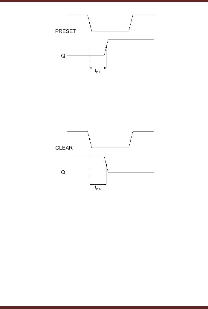
1. Propagtaion
Delay tPLH measured with respect to
the triggering edge of the
clock to the
low-to-high
transition of the output.
Figure 23.13. On a positive or
negative clock
transition
the
flip-flop changes its output
state. The Propagation Delay
is measured at 50%
transition
239
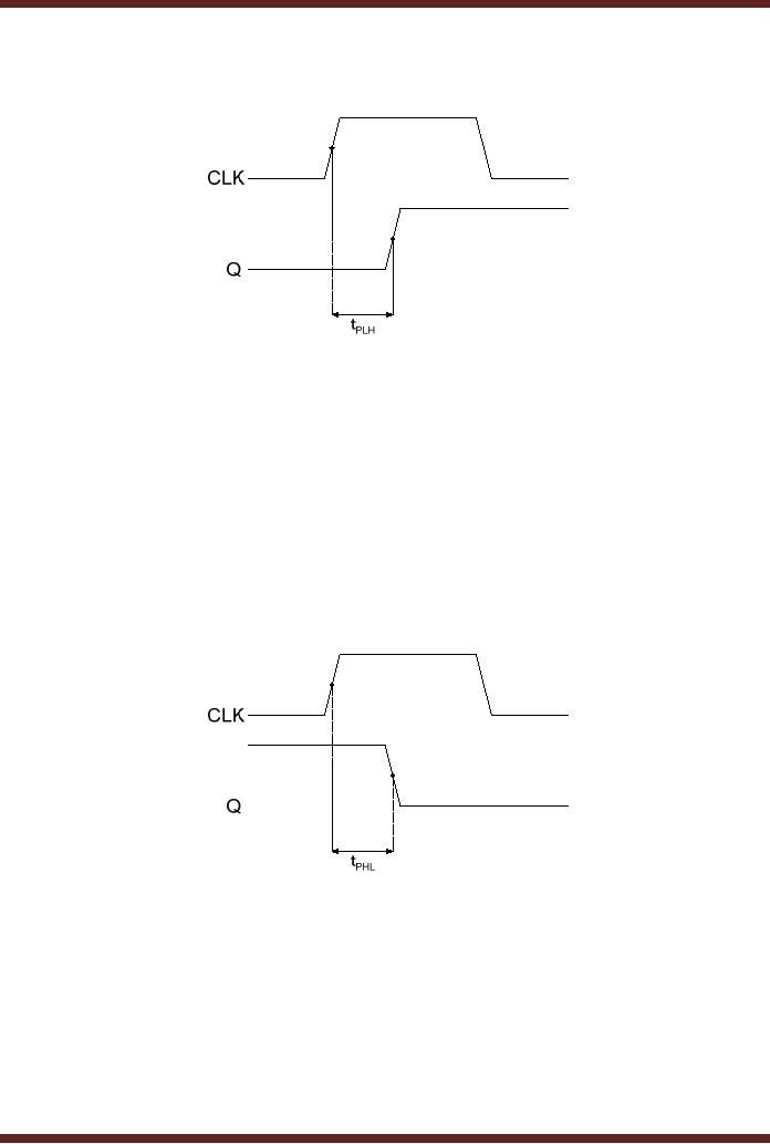
CS302 -
Digital Logic & Design
mark on
the triggering edge of the
clock and the 50%
mark on the low-to-high
transition of
the
output that occurs due to
the clock transition.
Figure
23.13 Propagation Delay,
clock to low-to-high transition of
the output
2. Propagtaion
Delay tPHL measured with respect to
the triggering edge of the
clock to the
high-to-low
transition of the output.
Figure 23.14. On a positive or
negative clock
transition
the
flip-flop changes its output
state. The Propagation Delay
is measured at 50%
transition
mark on
the triggering edge of the
clock and the 50%
mark on the high-to-low
transition of
the
output that occurs due to
the clock transition.
3. Propagtaion
Delay tPLH measured with respect to
the leading edge of the
preset input to the
low-to-high
transition of the output.
Figure 23.15. On a high-to-low
transition of the
preset
signal
the flip-flop changes its
output state to logic high.
The Propagation Delay
is
measured at
50% transition mark on the
triggering edge of the
preset signal and the
50%
mark on
the low-to-high transition of
the output that occurs
due to the preset
signal.
Figure
23.14 Propagation Delay,
clock to high-to-low transition of
the output
240
CS302 -
Digital Logic & Design
Figure
23.15 Propagation Delay,
preset to low-to-high transition of
the output
4. Propagtaion
Delay tPHL measured with respect to
the leading edge of the
clear input to the
high-to-low
transition of the output.
Figure 23.16. On a high-to-low
transition of the
clear
signal
the flip-flop changes its
output state to logic low.
The Propagation Delay
is
measured at
50% transition mark on the
triggering edge of the clear
signal and the
50%
mark on
the high-to-low transition of
the output that occurs
due to the preset
signal.
Figure
23.16 Propagation Delay,
clear to high-to-low transition of
the output
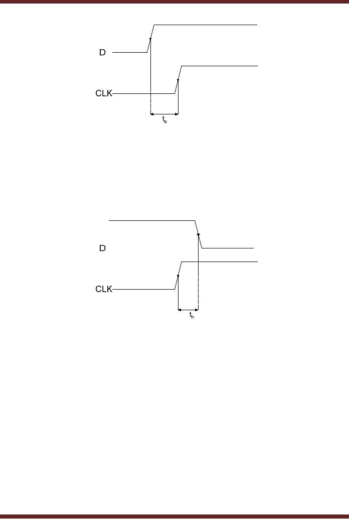
Set-up
Time
When a
clock transition occurs at
the clock input of a
flip-flop the output of the
flip-flop
is set to a
new state based on the
inputs. For the flip-flop to
change its output to a new
state at
the
clock transition, the input
should be stable. The
minimum time required for
the input logic
levels to
remain stable before the
clock transition occurs is
known as the Set-up time.
Figure
23.17.
241
CS302 -
Digital Logic & Design
Figure
23.17 Set-up time for a D
flip-flop
Hold
Time
The
input signal maintained at
the flip-flop input has to
be maintained for a
minimum
time
after the clock transition
for the flip-flop to
reliably clock in the input
signal. The minimum
time
for which the input
signal has to be maintained at
the input is the Hold
time of the
flip-flop.
Figure
23.18
Figure
23.18 Hold time for a D
flip-flop
Maximum
Clock Frequency
A flip-flop
can be operated at a certain
clock frequency. If the
clock frequency is
increased
beyond a certain limit the
flip-flop will be unable to
respond to the fast
changing
clock
transitions, therefore the
flip-flop will be unable to
function. The maximum
clock
frequency
fmax is the highest
rate at which the flip-flop
operates reliably.
Pulse
Width
A flip-flop
uses the clock, preset
and clear inputs for
its operation. Each signal
has to
be of a
specified duration for
correct operation of the
flip-flop. The manufacturer
specifies the
minimum
pulse width tw for
each of the three signals.
The clock signal is
specified by minimum
high
time and minimum low
time.
Power
Dissipation
A flip-flop
consumes power during its
operation. The power
consumed by a flip-flop is
defined by P =
Vcc x Icc.
The flip-flop is connected to +5
volts and it draws 5 mA of
current
during
its operation, therefore the
power dissipation of the
flip-flop is 25 mW.
242

CS302 -
Digital Logic & Design
A digital
circuit is made of a number of
gates, functional units and
flip-flops. The total
power
requirement of each device
should be known so that an
appropriate dc power source
is
used to
supply power to the digital
circuit.
243
Table of Contents:
- AN OVERVIEW & NUMBER SYSTEMS
- Binary to Decimal to Binary conversion, Binary Arithmetic, 1s & 2s complement
- Range of Numbers and Overflow, Floating-Point, Hexadecimal Numbers
- Octal Numbers, Octal to Binary Decimal to Octal Conversion
- LOGIC GATES: AND Gate, OR Gate, NOT Gate, NAND Gate
- AND OR NAND XOR XNOR Gate Implementation and Applications
- DC Supply Voltage, TTL Logic Levels, Noise Margin, Power Dissipation
- Boolean Addition, Multiplication, Commutative Law, Associative Law, Distributive Law, Demorgans Theorems
- Simplification of Boolean Expression, Standard POS form, Minterms and Maxterms
- KARNAUGH MAP, Mapping a non-standard SOP Expression
- Converting between POS and SOP using the K-map
- COMPARATOR: Quine-McCluskey Simplification Method
- ODD-PRIME NUMBER DETECTOR, Combinational Circuit Implementation
- IMPLEMENTATION OF AN ODD-PARITY GENERATOR CIRCUIT
- BCD ADDER: 2-digit BCD Adder, A 4-bit Adder Subtracter Unit
- 16-BIT ALU, MSI 4-bit Comparator, Decoders
- BCD to 7-Segment Decoder, Decimal-to-BCD Encoder
- 2-INPUT 4-BIT MULTIPLEXER, 8, 16-Input Multiplexer, Logic Function Generator
- Applications of Demultiplexer, PROM, PLA, PAL, GAL
- OLMC Combinational Mode, Tri-State Buffers, The GAL16V8, Introduction to ABEL
- OLMC for GAL16V8, Tri-state Buffer and OLMC output pin
- Implementation of Quad MUX, Latches and Flip-Flops
- APPLICATION OF S-R LATCH, Edge-Triggered D Flip-Flop, J-K Flip-flop
- Data Storage using D-flip-flop, Synchronizing Asynchronous inputs using D flip-flop
- Dual Positive-Edge triggered D flip-flop, J-K flip-flop, Master-Slave Flip-Flops
- THE 555 TIMER: Race Conditions, Asynchronous, Ripple Counters
- Down Counter with truncated sequence, 4-bit Synchronous Decade Counter
- Mod-n Synchronous Counter, Cascading Counters, Up-Down Counter
- Integrated Circuit Up Down Decade Counter Design and Applications
- DIGITAL CLOCK: Clocked Synchronous State Machines
- NEXT-STATE TABLE: Flip-flop Transition Table, Karnaugh Maps
- D FLIP-FLOP BASED IMPLEMENTATION
- Moore Machine State Diagram, Mealy Machine State Diagram, Karnaugh Maps
- SHIFT REGISTERS: Serial In/Shift Left,Right/Serial Out Operation
- APPLICATIONS OF SHIFT REGISTERS: Serial-to-Parallel Converter
- Elevator Control System: Elevator State Diagram, State Table, Input and Output Signals, Input Latches
- Traffic Signal Control System: Switching of Traffic Lights, Inputs and Outputs, State Machine
- Traffic Signal Control System: EQUATION DEFINITION
- Memory Organization, Capacity, Density, Signals and Basic Operations, Read, Write, Address, data Signals
- Memory Read, Write Cycle, Synchronous Burst SRAM, Dynamic RAM
- Burst, Distributed Refresh, Types of DRAMs, ROM Read-Only Memory, Mask ROM
- First In-First Out (FIFO) Memory
- LAST IN-FIRST OUT (LIFO) MEMORY
- THE LOGIC BLOCK: Analogue to Digital Conversion, Logic Element, Look-Up Table
- SUCCESSIVE APPROXIMATION ANALOGUE TO DIGITAL CONVERTER