 |
AND OR NAND XOR XNOR Gate Implementation and Applications |
| << LOGIC GATES: AND Gate, OR Gate, NOT Gate, NAND Gate |
| DC Supply Voltage, TTL Logic Levels, Noise Margin, Power Dissipation >> |
CS302 -
Digital Logic & Design
Lesson
No. 06
LOGIC
GATES & OPERATIONAL
CHARACTERISTICS
NOR
Gate as a Universal
Gate
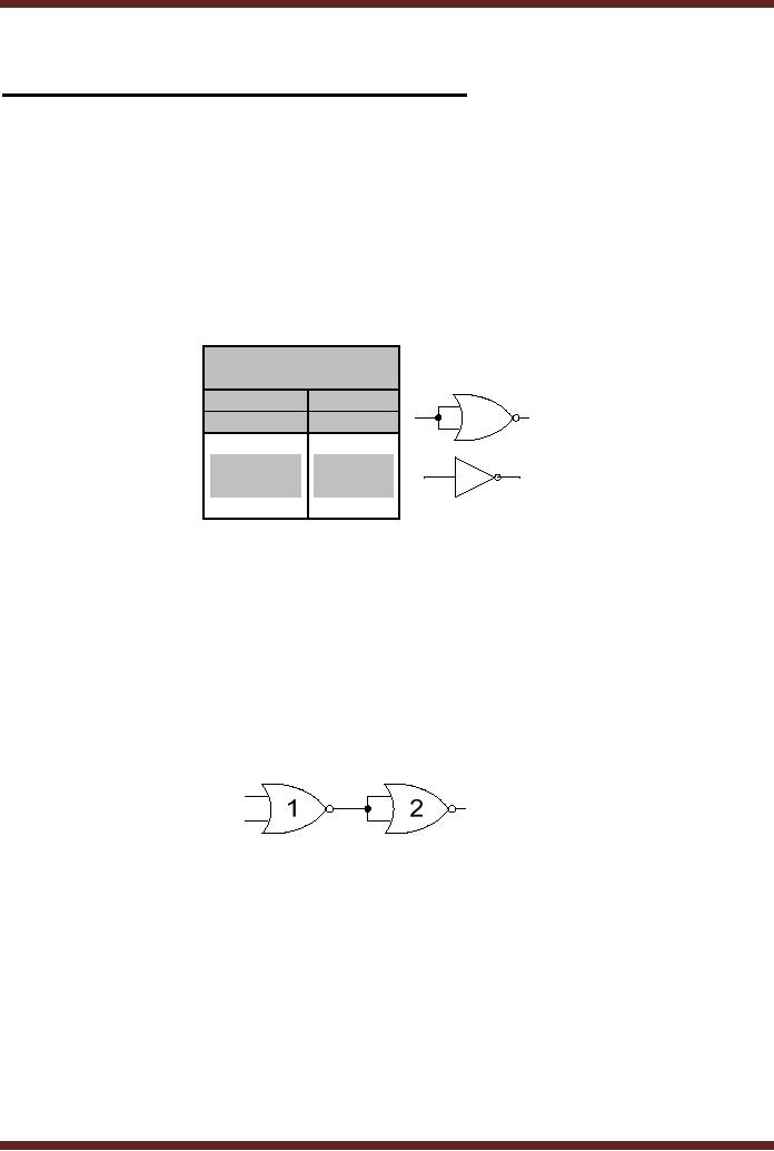
The
NOR gate is also used as a
Universal Gate as the NOR
Gate can be used in a
combination to
perform the function of a
AND, OR and NOT
gates.
4. NOT
Gate Implementation
A NOT
gate can be implemented
using a NOR gate by
connecting both the inputs
of
the
NOR gate together. By
connecting the two inputs
together, the combinations
with
dissimilar
inputs become redundant. The
Function Table of the
2-input NOR Gate reduces
to
that of
the NOT gate. Figure
6.1
Logical
NOR
Operation
Inputs
Output
A
B
F
0
0
1
0
1
0
1
0
0
1
1
0
Figure
6.1
Implementing a
NOT Gate using a NOR
gate
5. OR Gate
Implementation
A NOR
Gate performs the OR-NOT
function. Removing the NOT
gate at the output of
the
NOR gate results in an OR
gate. The effect of the
NOT gate at the output of
the NOR gate
can be
cancelled by connecting a NOT
gate at the output of the
NOR Gate. The two
NOT
gates
cancel each other out. A
NOT Gate implemented using a
NOR gate (2) is connected
to
the
output of a NOR gate (1).
Figure 6.2.
Figure
6.2
Implementing an
OR Gate using two NOR
gates
6. AND Gate
Implementation
An AND Gate
can be implemented using a
combination of three NOR
gates. The
implementation
is based on the alternate
symbolic representation of the AND
gate. The AND
gate is
represented as an OR gate with
bubbles at the inputs and
outputs. Figure 5.13.
The
two
bubbles at the input can be
replaced by two NOT gates
(1) & (2) implemented
using two
NOR
gates. If the two bubbles
are removed from the
two inputs, the OR gate
with the bubble
at the
output represents a NOR gate
(3). Figure 6.3
50
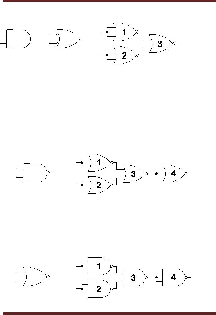
CS302 -
Digital Logic & Design
Figure
6.3
Implementing an
OR Gate using three NOR
gates
NAND-NOR
Universal Gates
NAND and
NOR gates are known as
Universal Gates as they can
be used to
implement
any of the three fundamental
gates, AND, OR and NOT.
The NAND Universal
Gate
can
also be used to implement a
NOR gate. Similarly, a NOR
gate can be used to
implement a
NAND
gate.
1. NAND
gate Implementation using
NOR gates
The AND
gate implementation using
three NOR gates is shown in
figure 6.3. A NAND
gate
implementation requires addition of an
inverter (NOT) gate at the
output. The NOT gate
is
implemented
using a NOR gate. Figure
6.4. NOR gates 1, 2 and 3
implement the AND
gate.
NOR
gate 4 implements the NOT
gate connected at the output
of the NAND gate.
Figure
6.4
Implementing a
NAND Gate using four NOR
gates
2. NOR
gate Implementation using
NAND gates
The OR
gate implementation using
three AND gates is shown in
figure 5.20. A NOR
gate
implementation requires addition of an
inverter (NOT) gate at the
output. The NOT gate
is
implemented
using a NAND gate. Figure
6.5. NAND gates 1, 2 and 3
implement the OR
gate.
NAND gate 4
implements the NOT gate
connected at the output of
the NOR gate.
Figure
6.5
Implementing a
NOR Gate using four NAND
gates
51

CS302 -
Digital Logic & Design
NAND
and NOR Gate
Applications
The
output of a NAND is 0 when all
inputs to the NAND gate are
1s. This property of
the NAND
gate can be used to activate
an operation when any of the
inputs to the NAND
gate
are
deactivated. A NOR gate on
the other hand generates an
output of 1 when all inputs
to
NOR
gate are deactivated. The
output is deactivated when
any input is
activated.
A warehouse is
used to store industrial
chemicals. Toxic fumes
produced by the
chemicals
are removed from the
ware house and dispersed in
the atmosphere through
three
exhaust
fans. The three exhaust
fans should be continuously
working to remove the
dangerous
toxic fumes. If any one or
more fans fail an alarm
should be activated to signal
the
failure of
one or more exhaust
fans.
An electronic
circuit connected to each
fan generates a 1 to indicate a
working fan. If
the
fan fails the circuit
generates a 0 output. The
outputs of the three fans
are connected to the
three
inputs of a NAND gate. When
all fans are working
the input to the 3-input
NAND gate is
111
and the corresponding output
is a 0. When any one fan
fails the output of NAND
gate
becomes 1
activating an alarm connected to
the output of the NAND gate.
Figure 6.6
Figure
6.6
A NAND gate
based exhaust fan failure
detection system
A Washing
Machine has three sensors to
check for washing machine
lid open, washing
tub
filled to minimum level and
weight of cloths and water
in the tub. If the lid of
the Washing
machine is
open or the water is below
the minimum level or the
washing machine has
been
overloaded
the appropriate sensor
generates an output of 1. The
outputs of the three
sensors
are
connected to the inputs of a
3-input NOR gate. During
the normal operation of
the
Washing
Machine all the sensors
output a 0. The corresponding
output of the NOR gate is a
1.
If an erroneous
condition is detected by any
one or more sensors, the
corresponding sensor
output(s) is
set to 1, setting the NOR
gate output to a 0. The NOR
gate output is connected
to
the
main switch which switches
off the washing machine.
Figure 6.7.
Figure
6.7
A NOR
gate based Washing Machine
Controller
52

CS302 -
Digital Logic & Design
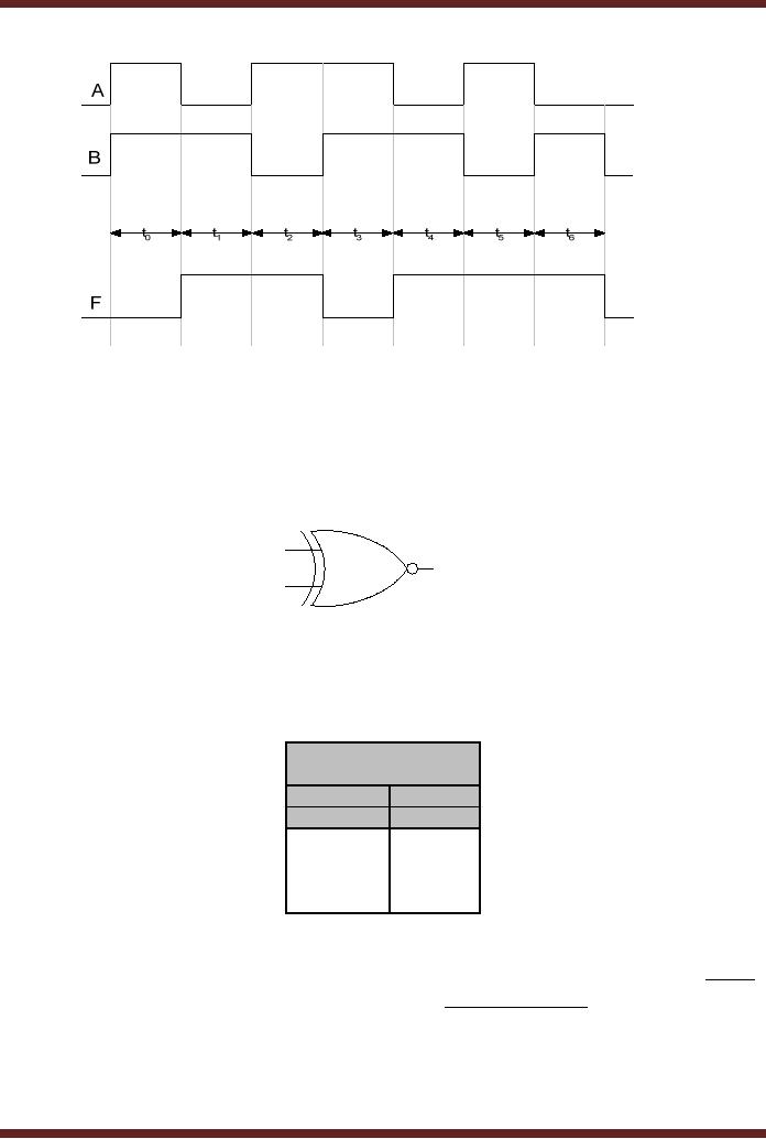
Exclusive-OR
and Exclusive-NOR
Gates
The
XOR and XNOR gates
are frequently used in
Digital Logic. These two
additional
gates
are used to detect
dissimilar and similar
inputs respectively.
1. Exclusive-OR
Gate
The
Exclusive-OR Gate or XOR
Gate performs a function
that is equivalent to
the
combination of
NOT, AND and OR gates. XOR
gates are extensively used
in digital
applications;
therefore XOR gates are
available as basic components.
Most commonly used
XOR
Gates have two inputs.
The XOR gate is represented
by symbol shown in figure
6.8.
Figure
6.8
Symbolic
representation of XOR
Gate
The
function performed by the
XOR gate is represented by
the Function Table for
a
two
input XOR Gate. Figure
6.9. The function table
for a 3, 4 or multiple input
XOR Gate is
similar.
The output of an XOR gate is
1 when the inputs are
dissimilar and a 0 when all
the
inputs
are the same.
Logical
XOR
Operation
Inputs
Output
A
B
F
0
0
0
0
1
1
1
0
1
1
1
0
Figure
6.9
Function
Table of an XOR Gate
The
expression describing the
operation of the two inputs
XOR Gate is F = A ⊕ B . The
⊕ is an XOR
operator and the expression
for multiple input XOR
Gates is
F = A ⊕ B ⊕ C ⊕ .....N , where N is the
total number of
inputs.
The
timing diagram of the two
input XOR gate with
the input varying over a
period of 7
time
intervals is shown in the
diagram. Figure 6.10.
53
CS302 -
Digital Logic & Design
Figure
6.10
Timing
diagram of operation of a XOR
gate
2. Exclusive-NOR
Gate
The
Exclusive-NOR Gate or XNOR
Gate performs a function
that is equivalent to
the
combination of
NOT, AND and OR gates. XNOR
gate is extensively used in
digital
applications;
therefore XNOR gates are
available as basic components.
Most commonly used
XNOR
Gates have two inputs.
The XNOR gate is represented
by symbol shown in figure
6.11.
Figure
6.11
Symbolic
representation of XNOR
Gate
The
function performed by the
XNOR Gate is represented by
the Function Table for
a
two
input XNOR Gate. Figure
6.12. The function table
for a 3, 4 or multiple input
XNOR Gate
is similar.
The output of an XNOR gate
is 1 when the all the
inputs are same and a 0
when the
inputs
are dissimilar.
Logical
XNOR
Operation
Inputs
Output
A
B
F
0
0
1
0
1
0
1
0
0
1
1
1
Figure
6.12
Function
Table of an XNOR Gate
The
expression describing the
operation of the two inputs
XNOR Gate is F = A ⊕ B .
The
expression for multiple
input XNOR Gates is F = A ⊕ B ⊕ C ⊕ .....N , where N is the
total
number of
inputs.
The
timing diagram of the two
input XNOR gate with
the input varying over a
period of
7 time
intervals is shown in the
diagram. Figure 6.13.
54
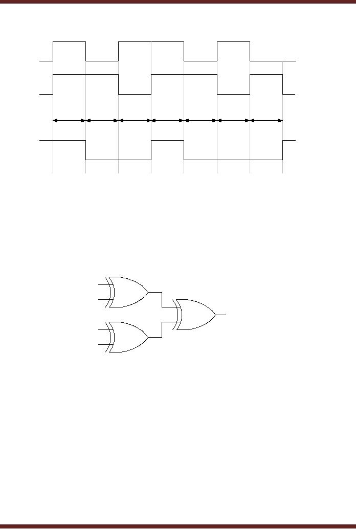
CS302 -
Digital Logic & Design
A
B
t0
t1
t2
t3
t4
t5
t6
F
Figure
6.13
Timing
diagram of operation of a XNOR
gate
XOR
and XNOR Gate
Applications
XOR
and XNOR gates are
used to detect dissimilar
and similar inputs. This
property of
XOR
and XNOR gates is used to
detect odd and even
number of 1s in a Parity
Detection
Circuit.
Consider
the three XOR gate
logic circuit which is used
to detect odd number of 1's
in
a 4-bit
binary input combination.
Figure 6.14
A
1
B
3
C
2
D
Figure
6.14
XOR
gate based Odd number of 1s
detector
A 4-bit
binary number 0000 applied
at the inputs A, B, C and D
respectively of XOR
gates 1
and 2. The output of XOR
Gates 1 and 2 is 0 and 0.
The output of XOR gate 3 is
also
zero.
Similarly, a binary number
0011 applied at the inputs
A, B, C and D respectively.
The
output of
XOR gate 1 with inputs 00 is
0. The output of XOR gate 2
with inputs 11 is 0.
The
output of
gate 3 is 0. Thus the output
indicates that the binary
number 0011 does not
have odd
number of
1's. Consider the binary
number 1011 applied at the
inputs A, B, C and D
respectively.
The output of XOR gate 1
with inputs 10 is 1. The
output of XOR gate 2
with
inputs 11 is 0.
The output of gate 3 is 1.
Thus the output indicates
that the binary number
1011
has
odd number of 1's
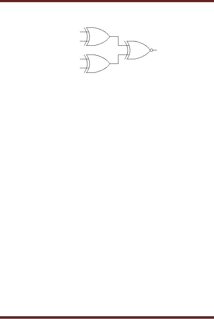
The
logic circuit based on two
XOR and a single XNOR
gate which is used to
detect
even
number of 1's in a 4-bit
binary input combination.
Figure 6.15
55
CS302 -
Digital Logic & Design
A
1
B
3
C
2
D
Figure
6.15
XOR-XNOR
gate based Even number of 1s
detector
A 4-bit
binary number 0000 applied
at the inputs A, B, C and D
respectively of XOR
gates 1
and 2. The output of XOR
Gates 1 and 2 is 0 and 0.
The output of XNOR gate 3 is
a 1.
Similarly, a
binary number 0011 applied
at the inputs A, B, C and D
respectively. The output
of
XOR
gate 1 with inputs 00 is 0.
The output of XOR gate 2
with inputs 11 is 0. The
output of
XNOR
gate 3 is also a 1. Thus the
output indicates that the
binary number 0011 has
even
number of
1's. Consider the binary
number 1011 applied at the
inputs A, B, C and D
respectively.
The output of XOR gate 1
with inputs 10 is 1. The
output of XOR gate 2
with
inputs 11 is 0.
The output of XNOR gate 3 is
0 because of dissimilar inputs.
Thus the output
indicates
that the binary number
1011 does not have
even number of 1's.
Digital
Circuits and Operational
Characteristics
The
Logic Gates discussed
provide the basic building
blocks for implementing the
large
digital
systems. The logic gates
discussed so far has been
described in terms of the
functions
they
perform. Practical implementation of
digital systems by using the
logic gates in
combination
requires some additional
information. For example,
theoretically the output of
an
Inverter
can be connected to the
inputs of an unlimited number of AND
Gates. However, the
practical
limitation to the circuit
shown is that the total
current sourced by the
Inverter is
distributed
amongst the 10 AND Gates.
The Inverter is not able to
provide the total
current
required by
the ten AND gates. The
current sunk by each AND
gate is not enough to drive
the
AND gate
circuitry thus its behavior
is unpredictable resulting in
unpredictable behavior of
the
system.
The
binary 1 and 0 are
represented by +5V and 0 V.
What if the output of an AND
Gate
is +3 V? Does
this output voltage level
represent a binary 1 or 0? If the
output of the AND
Gate
is connected to
the input of an Inverter,
what would be the response
of the Inverter?
Another
important
aspect is the frequency of
the input signal. Electronic
circuits operate at
certain
frequencies. If
the frequency of the input
signal increases beyond the
operational specification
of the
circuit, the circuit will
not be able to respond fast
enough resulting in
unpredictable
behavior.
Digital
circuits that depend upon
battery for their power
should consume low power
to
allow
the device to function for
longer periods of time
before replacing or recharging
the
battery.
Thus the digital system
should be implemented keeping in
view the power
requirements of
the application.
56

CS302 -
Digital Logic & Design
TTL/CMOS
NOT Gate
Operation
Logic
Gates are implemented using
transistors. These transistors
are connected in
various
combinations to form a switching
circuit. The transistor
itself is configured to work
like
a switch. On
the application of a bias
voltage the transistor is
switched on and by removing
the
bias
voltage the transistor is
turned off. Different
technologies are used to
manufacture the
Logic
Gates based on the
transistors. The performance or
the Operational characteristics of
a
Logic
Gate are determined by the
transistors and the
technologies used to implement
the
switching
transistors. Certain technologies
allow transistor and thereby
the Logic Gates to
operate at
high frequencies. Other
technologies allow transistors to
operate with low
voltages,
consuming
minimal power, similarly
certain other implementation
technologies allow
very
dense
logic circuits to be
manufactured.
The
Inversion function of the
NOT gate is performed by the
switching circuit
shown
in figure
6.16. The Bipolar Junction
Transistor (BJT) based NOT
shown on the left is
switched
on when a
Voltage is applied at the
base of the BJT. The
transistor when switched on
short
circuits
the VCC, the output
voltage is therefore 0 volts.
When the BJT base
pin is connected to
0 volts,
the transistor is switched
off. The Vo/p is
at potential VCC
= 5 Volts.
The actual
implementation
is different.
Figure
6.16
BJT &
CMOS based NOT Gate
Implementation
The
CMOS based implementation,
shown on the right, uses a
P-type and a N-type
MOSFETs.
When the input is connected
to +V, the P-type MOSFET is
switched off and the
N-
type
MOSFET is switched on. The
Vo/p is at ground
potential. When the input is
connected to
ground,
the P-type and N-type
MOSFETs are switched on and
off respectively. The Vo/p is at
potential
VDD = 5 Volts.
Integrated
Circuit Technologies
The
practical implementation of the
Logic gates is through the
Integrated Circuits
(IC)
technologies.
The logic gates implemented
through these technologies
are available to be
connected
and practical implementation of a
digital circuit. Different
types of Integrated
Circuit
technologies
are used to implement the
digital circuits. These
technologies differ in terms
of
the
circuit density, power
consumptions, frequency response
etc.
·
CMOS:
Complementary Metal-Oxide
Semiconductor
57

CS302 -
Digital Logic & Design
The
most extensively used
technology, characterized by low
power consumption,
switching
speed which is slower but
comparable to TTL. Has
higher chip density
than
TTL.
Due to high input impedance
is easily damaged due to
accumulated static
charge
·
TTL:
Transistor-Transistor Logic
Extensively
used technology, characterized by
fast switching speed and
high power
consumption
Offers a
wide variety of gates,
devices, arithmetic units
etc.
·
ECL:
Emitter-Coupled Logic
Used in
specialized applications where
switching speed is of prime
importance such as
high
speed transmission, high
speed memories and high
speed arithmetic
units.
·
PMOS:
p-channel and NMOS:
n-channel MOS transistor
PMOS
and NMOS technologies are
used in LSI requiring high
chip density. Large
memories
and microprocessors are
implemented using these
technologies
These
ICs have very low
power consumption.
2
·
E CMOS: a
combination of CMOS and NMOS
technologies
Used to
implement Programmable Logic
Devices
Types of IC
Logic Gates
The
most common form of logic
Gate ICs are listed. To
identify and use the
Integrated
Circuits or
ICs in implementing logic
circuits, some sort of
identification code has to be
used
which is
printed on the IC
package.
Logic
Gates are identified by the
codes. The prefix 74 is used
to identify a commercial
version of
the device from the
military version device
identified by the prefix 54.
Military
versions
are designed to withstand
harsh and severe
environmental conditions. The XX
part of
the
code identifies the
switching speed of the
gate.
74XX00
Quad
2-input NAND Gate
o
74XX02
Quad
2-input NOR Gate
o
74XX04
Hex
Inverter
o
74XX08
Quad
2-input AND Gate
o
74XX10
Triple
3-input NAND Gate
o
74XX11
Triple
3-input AND Gate
o
74XX20
Dual
4-input NAND Gate
o
74XX21
Dual
2-input AND Gate
o
74XX27
Triple
3-input NOR Gate
o
74XX30
Single
8-input NAND Gate
o
74XX32
Quad
2-input OR Gate
o
74XX86
Quad
2-input XOR Gate
o
74XX133
Single
13-input NAND Gate
o
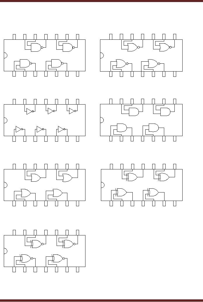
The
Integrated Circuit packages of
the seven gates that
have been discussed so
far
are
shown. Figure 6.17. The
7408 14-pin chip has 4 or
Quad, 2-input AND gates. The
input
pins
and the output pins of
each of the four gates
are shown. To use any
one or all four
gates
the
appropriate pins are
connected. Pins 7 and 14 are
connected to ground and
Supply
voltage
respectively.
The
7432 14-pin IC package has 4
or Quad, 2-input OR Gates.
Connections to the OR
gates
are identical to those of
the 7408 AND gate IC.
The 7404 14-pin chip
has 6 or hex,
inverters.
The input and output
connections of each of the 6
NOT gates are shown.
Pins 7 and
14 are
used for ground and
supply voltage
respectively.
58
CS302 -
Digital Logic & Design
The
7400, Quad, 2-input NAND
Gate IC, the 7402,
Quad, 2-input NOR Gate
IC, the
7486,
Quad, 2-input XOR Gate IC
and the 74266, Quad,
2-input XNOR Gate IC are
similar.
12
11
8
14
13
10
9
14
13
12
11
10
9
8
1
2
3
4
5
6
7
1
2
3
4
5
6
7
7400
7402
Four
2-Input NAND Gate
Four
2-Input NOR Gate
12
11
8
14
13
10
9
14
13
12
11
10
9
8
7
1
2
3
4
5
6
7
1
2
3
4
5
6
7408
7404
Four
2-Input AND Gate
Hex
Inverters
14
13
12
11
10
9
8
14
13
12
11
10
9
8
7
7
1
2
3
4
5
6
1
2
3
4
5
6
7432
7486
Four
2-Input OR Gate
Four
2-Input XOR Gate
14
13
12
11
10
9
8
7
1
2
3
4
5
6
74266
Four
2-Input XNOR Gate
Figure
6.17
Commonly
used Integrated Circuit
Logic Gates
59

CS302 -
Digital Logic & Design
Performance
Characteristics and
Parameters
A number of
performance characteristics and
parameters determine the
suitability of a
particular IC
technology for a particular
application. The important
parameters that are
considered
whilst designing Digital
Logic Circuits are mentioned
briefly.
· DC Supply
Voltage:
o The
supply voltage at which the
Gate operates
· Noise
Margin:
o The
maximum and minimum voltages
that represent binary 0 and
1 respectively. These
voltage
ranges determine the
suitability of a gate to work in
noisy environments.
· Power
Dissipation:
o Gates
consume power during their
operation. The power
dissipation varies with
the
frequency at
which these gates
operate.
· Frequency
Response and Propagation
Delay:
o Gates do
not instantaneously switch to a
new output state after
the inputs are
changed.
The
delay between the input
and output limits the
frequency at which the
inputs to a
logic
gate can be changed and
the logic circuit can
operate.
· Fan-Out:
o The
number of gates that can be
connected to the output of a
single gate.
60
Table of Contents:
- AN OVERVIEW & NUMBER SYSTEMS
- Binary to Decimal to Binary conversion, Binary Arithmetic, 1s & 2s complement
- Range of Numbers and Overflow, Floating-Point, Hexadecimal Numbers
- Octal Numbers, Octal to Binary Decimal to Octal Conversion
- LOGIC GATES: AND Gate, OR Gate, NOT Gate, NAND Gate
- AND OR NAND XOR XNOR Gate Implementation and Applications
- DC Supply Voltage, TTL Logic Levels, Noise Margin, Power Dissipation
- Boolean Addition, Multiplication, Commutative Law, Associative Law, Distributive Law, Demorgans Theorems
- Simplification of Boolean Expression, Standard POS form, Minterms and Maxterms
- KARNAUGH MAP, Mapping a non-standard SOP Expression
- Converting between POS and SOP using the K-map
- COMPARATOR: Quine-McCluskey Simplification Method
- ODD-PRIME NUMBER DETECTOR, Combinational Circuit Implementation
- IMPLEMENTATION OF AN ODD-PARITY GENERATOR CIRCUIT
- BCD ADDER: 2-digit BCD Adder, A 4-bit Adder Subtracter Unit
- 16-BIT ALU, MSI 4-bit Comparator, Decoders
- BCD to 7-Segment Decoder, Decimal-to-BCD Encoder
- 2-INPUT 4-BIT MULTIPLEXER, 8, 16-Input Multiplexer, Logic Function Generator
- Applications of Demultiplexer, PROM, PLA, PAL, GAL
- OLMC Combinational Mode, Tri-State Buffers, The GAL16V8, Introduction to ABEL
- OLMC for GAL16V8, Tri-state Buffer and OLMC output pin
- Implementation of Quad MUX, Latches and Flip-Flops
- APPLICATION OF S-R LATCH, Edge-Triggered D Flip-Flop, J-K Flip-flop
- Data Storage using D-flip-flop, Synchronizing Asynchronous inputs using D flip-flop
- Dual Positive-Edge triggered D flip-flop, J-K flip-flop, Master-Slave Flip-Flops
- THE 555 TIMER: Race Conditions, Asynchronous, Ripple Counters
- Down Counter with truncated sequence, 4-bit Synchronous Decade Counter
- Mod-n Synchronous Counter, Cascading Counters, Up-Down Counter
- Integrated Circuit Up Down Decade Counter Design and Applications
- DIGITAL CLOCK: Clocked Synchronous State Machines
- NEXT-STATE TABLE: Flip-flop Transition Table, Karnaugh Maps
- D FLIP-FLOP BASED IMPLEMENTATION
- Moore Machine State Diagram, Mealy Machine State Diagram, Karnaugh Maps
- SHIFT REGISTERS: Serial In/Shift Left,Right/Serial Out Operation
- APPLICATIONS OF SHIFT REGISTERS: Serial-to-Parallel Converter
- Elevator Control System: Elevator State Diagram, State Table, Input and Output Signals, Input Latches
- Traffic Signal Control System: Switching of Traffic Lights, Inputs and Outputs, State Machine
- Traffic Signal Control System: EQUATION DEFINITION
- Memory Organization, Capacity, Density, Signals and Basic Operations, Read, Write, Address, data Signals
- Memory Read, Write Cycle, Synchronous Burst SRAM, Dynamic RAM
- Burst, Distributed Refresh, Types of DRAMs, ROM Read-Only Memory, Mask ROM
- First In-First Out (FIFO) Memory
- LAST IN-FIRST OUT (LIFO) MEMORY
- THE LOGIC BLOCK: Analogue to Digital Conversion, Logic Element, Look-Up Table
- SUCCESSIVE APPROXIMATION ANALOGUE TO DIGITAL CONVERTER