 |
16-BIT ALU, MSI 4-bit Comparator, Decoders |
| << BCD ADDER: 2-digit BCD Adder, A 4-bit Adder Subtracter Unit |
| BCD to 7-Segment Decoder, Decimal-to-BCD Encoder >> |
CS302 -
Digital Logic & Design
Lesson
No. 16
16-BIT
ALU
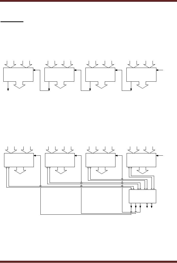
Consider
the four ALUs connected to
form a 16-bit ALU without
the Look-Ahead Carry
circuit.
Figure 16.1. The ALU1
will only generate an output
and a Carry Out 8 when it
has
received an
input at Carry In 4. Similarly,
ALU2 will only generate an
output and a Carry
Out
12 when it
has received Carry In 8.
Finally, the Carry Out 16 is
generated only when ALU3
has
received
Carry In 12. Thus the
Carry instead of rippling
through the 4-bits of the
individual ALU
circuit
has to propagate through
four ALU units. The last ALU
unit has to wait until it
receives
the
Carry propagating through
each of the three
units.
Cin8
Cin4
Cin0
Cin12
ALU3
ALU2
ALU1
ALU0
Cout16
Cout12
Cout8
Cout4
Figure
16.1
Carry
Propagation Delay between
4-bit ALU units
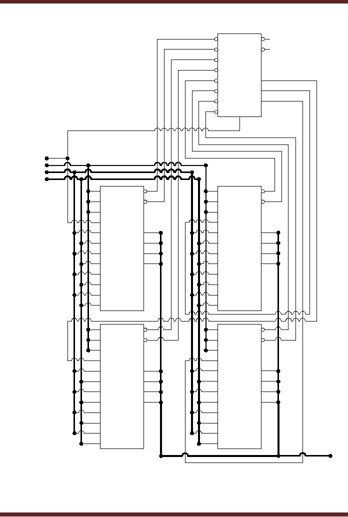
The
delay caused by the Carry
Propagating through the four
units is eliminated by
the
Group
Carry terms used by the
381 ALUs. Figure 16.2.
Instead of the Carry Out
each ALU
generates
Group-Carry Generate and
Propagate terms, which
indicate if the most
significant
Carry is
generated by the 4-bit ALU or
otherwise. The Group Carry
terms are connected to
the
Look-Ahead
Carry Generator which
generates the Cary bits
C1, C2 and C3 which
are
connected to
Cin4, Cin8 and Cin12
respectively. Thus Carry no
longer propagates through
the
ALU
units.
Cin8
Cin4
Cin0
Cin12
ALU3
ALU2
ALU1
ALU0
G3
P3
G2
P2
G1
P1
G0
P0
G3 P3 G2 P2 G1 P1 G0
P0
Look-Ahead
Carry
Generator
C3
C2
C1
G
P
Figure
16.2
Carry
Propagation Delay eliminated by
using Group Carry
The G
output is activated if the
4-bit unit generates a Carry
Out irrespective of Carry
In.
The P
output is activated if the
4-bit unit generates a Carry
Out if the Carry In is
active. The
Look-Ahead
circuit implemented earlier is
based on Logic Gates, where
the Look-Ahead Carry
150

CS302 -
Digital Logic & Design
Generator
circuit has P0, P1, P2 and P3 Carry Propagate and
G0, G1, G2 and G3
Carry
Propagate
Inputs and C1, C2, C3 and C4 Carry Out outputs.
The 74XX182 is the MSI
version of
the
Look-Ahead Carry Generator,
which provides identical
inputs and outputs except
for the C4
output
which is available in the
form of P and G output pins
to allow a second level
Cascading.
The
connection of four 74XX381
4-bit ALUs and a 74XX182 to
implement a 16-bit ALU is
shown.
Figure 16.3
The
inputs A, B and the output F
of the four, 4-bit ALUs 0,
1, 2 and 3 are connected
to
appropriate
bits of the 16-bit inputs A,
B and output F respectively.
Thus bits A(0-3),
B(0-3)
and
F(0-3) are connected to
inputs and output of ALU0,
bits A(4-7), B(4-7) and
F(4-7) are
connected to
inputs and output of ALU1,
bits A(8-11), B(8-11) and
F(8-11) are connected
to
inputs
and output of ALU2 and
bits A(12-15), B(12-15) and
F(12-15) are connected to
inputs
and
output of ALU3. The
Group-Carry Generate and
Propagate outputs of the
four ALUs are
connected to
the inputs of Look-Ahead
Carry generator 74X182
respectively. The
Carry
outputs
C1, C2 and C3 from the
Look-Ahead Carry generator
circuit are generated after
a gate
delay of 2
and are connected to the
Carry in pins of ALUS 1, 2
and 3 respectively.
151
CS302 -
Digital Logic & Design
G
G0
6
P
P0
74X182
G1
P1
C4
G2
C1
C8
P2
C2
C12
G3
C3
P3
C0
C0
S(0-2)
A(0-15)
B(0-15)
S0
S0
S0
G
S0
G
S1
P2
S1
P0
S1
P
S1
P
74X381
74X381
S2
S2
S2
S2
Cin
Cin
F0
F8
A0
A8
F0
F0
A0
A0
F1
F9
B0
B8
F1
F1
B0
B0
F2
F10
A1
A9
F2
F2
A1
A1
F3
F11
B1
B9
F3
F3
B1
B1
A2
A10
A2
A2
B2
B10
B2
B2
ALU0
ALU2
A3
A11
A3
A3
B3
B11
B3
B3
S0
S0
S0
S0
G
G
S1
P1
S1
P3
S1
P
S1
P
74X381
74X381
S2
S2
S2
S2
Cin
Cin
A12
F12
F4
A4
A0
F0
F0
A0
B12
F13
B4
F5
B0
F1
F1
B0
A13
F14
A5
F6
A1
F2
A1
F2
B13
F15
B5
F7
B1
F3
B1
F3
A6
A14
A2
A2
B6
B14
B2
B2
ALU1
ALU3
A7
A15
A3
A3
B7
B15
B3
B3
F(0-15)
Figure
16.3
16-bit
ALU
Comparators
152
CS302 -
Digital Logic & Design
The
basic function of a Comparator is to
compare two binary
quantities and to
determine if
the two quantities are
equal. If the quantities are
not equal then it has
to
determine
which of the two quantities
is greater than the other.
Many Integrated Circuit
Comparators
have three outputs to
indicate A=B, A>B and
A<B.
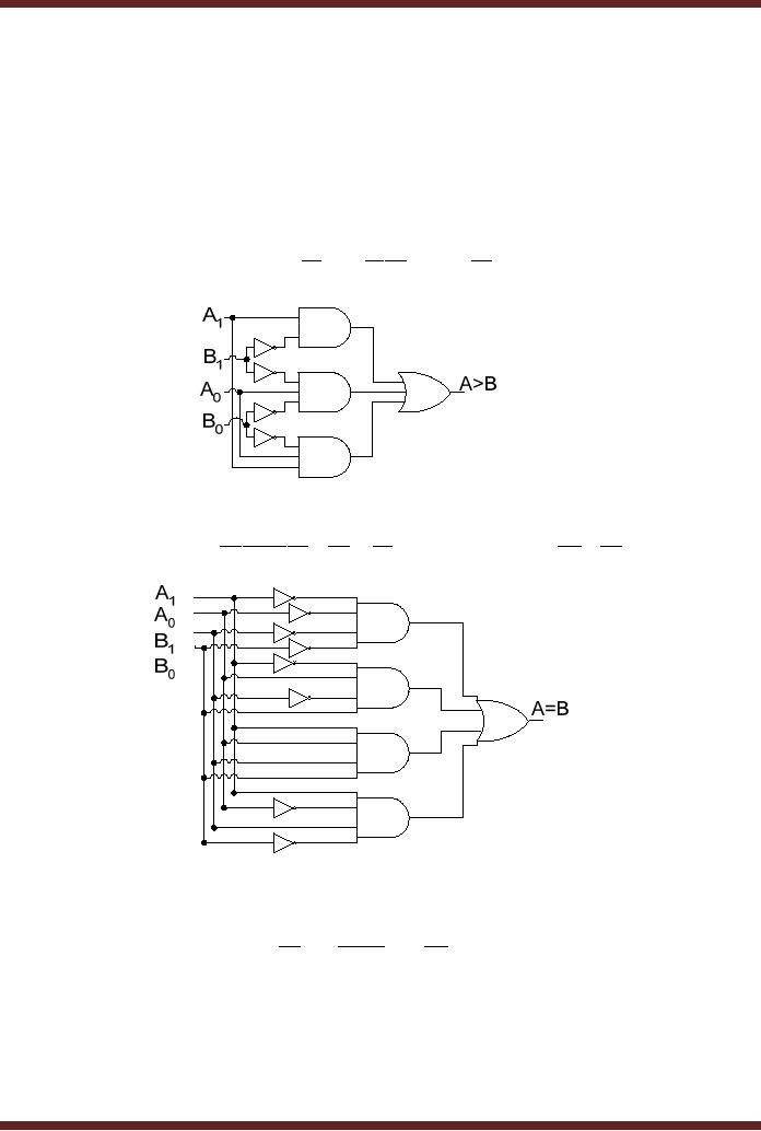
Earlier,
simplified Boolean expressions
for a 2-bit Comparator
circuit were
determined
that
compares two 2-bit numbers
and sets one of its
three outputs to indicate
A=B, A>B or
A<B.
The Booleans expressions
representing the three
outputs are presented. The
three
Combinational
Circuits implementing the
three outputs are also
shown. Figure 16.4
(A > B) = A 1B1 + A 0 B1B 0 + A 1A 0 B 0
Figure
16.4a Implementation of
A>B
(A = B) = A 1 A 0 B1B 0 + A 1A 0 B1B 0 + A 1A 0B1B 0 + A 1 A 0B1B 0
Figure
16.4b Implementation of
A=B
(A < B) = A 1B1 + A 1 A 0B 0 + A 0B1B 0
153
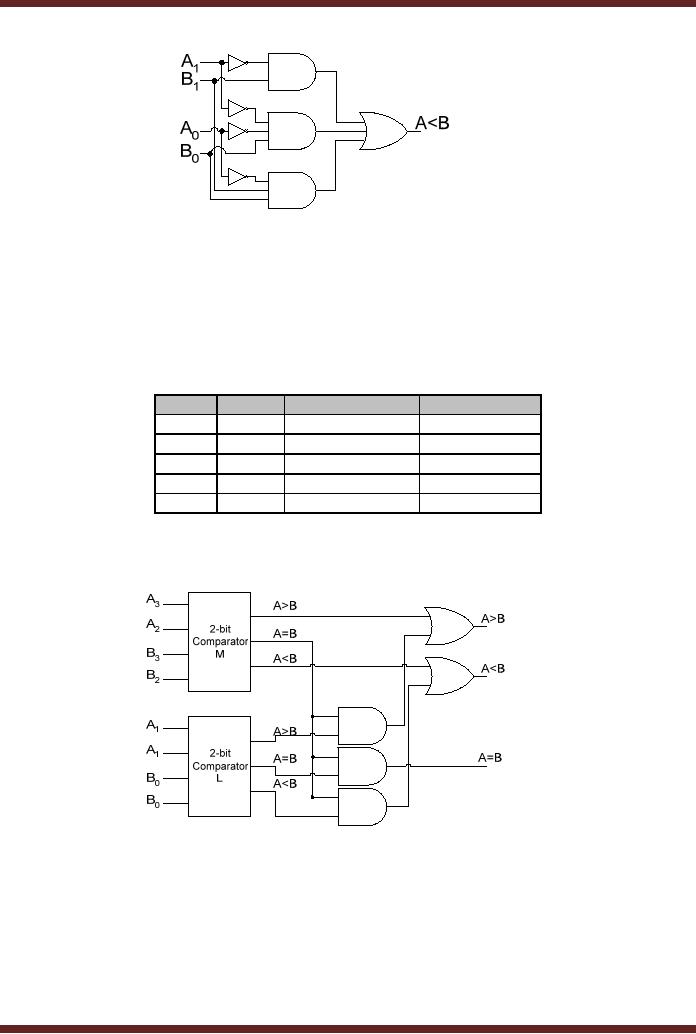
CS302 -
Digital Logic & Design
Figure
16.4c Implementation of
A<B
The
2-bit Comparator discussed
earlier is considered to be a Parallel
Comparator as all
the
bits are compared
simultaneously. External Logic
has to be used to Cascade
together two
such
Comparators to form a 4-bit
Comparator.
The
4-bit numbers compared by
the Cascaded implementation
are represented in
table
16.1.
A
B
Comparator
M
Comparator
L
1101
0111
A>B
0110
1011
A<B
0011
0010
A=B
A>B
0100
0101
A=B
A<B
1001
1001
A=B
A=B
Table
16.1
Comparison of
numbers by Cascaded 4-bit
Comparator
Figure
36.5
Implementation
of 4-bit Comparator by Cascading
two 2-bit Comparators
The
two most significant bits of
4-bit numbers A and B are
compared by the Most
Significant
2-bit Comparator M and the
least significant two bits
are compared by the
Least
Significant
2-bit Comparator L. Figure
16.5 If the two most
significant bits of number A
are
greater
than the two most
significant bits of number B,
(A=1101 and B =0111) the
Most
Significant
Comparator indicates A>B
and there is no need to
compare the remaining two
least
significant
bits. Similarly, if the two
most significant bits of
numbers A and B (A=0110
and
B=1011)
are compared by the Most
Significant Comparator and
the comparator sets its
A<B
154
CS302 -
Digital Logic & Design
then
there is no need to compare
the remaining two least
significant bits. However, if
the two
most
significant bits of numbers A
and B indicates A=B then
least significant two bits
have to
be compared to
determine if A>B (A=0011
B=0010), A<B (A=0100
B=0101) or A=B
(A=1001
B=1001).
Thus the A=B output of
the Most Significant 2-bit
Comparator is used to enable
three
AND gates.
The output of only one AND
gate is set to 1 depending
upon the output of
the
Least
Significant 2-bit
Comparator.
An alternate
method of implementing Comparators
which allows the Comparators
to be
easily
cascaded without the need
for extra logic gates by
Iterative Circuit based
Comparators.
Iterative
Circuit based
Comparator
An Iterative
circuit is implemented using
identical modules each of
which has Primary
Inputs
and Outputs and Cascading
Inputs and Outputs. The
Cascading inputs of the
least
significant
module are connected to
fixed logic inputs and
the Cascading outputs
are
connected to
the Cascading inputs of the
next significant module. A
2-bit Iterative
Circuit
based
Comparator is shown. Figure
16.6.
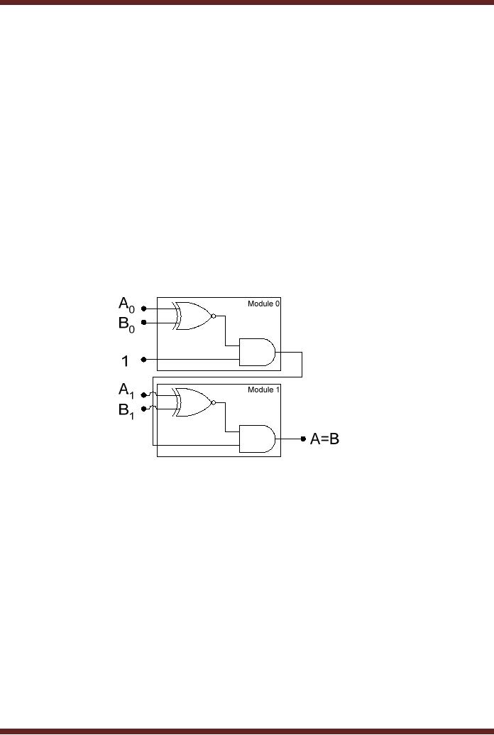
Figure
16.6a Iterative Circuit
Implementation of A=B
function
The
Cascading input of Module 0 is
connected to logic 1. If input
A0 is equal to input
B0,
the
XNOR gate output in Module 0
is a 1 which is passed on to Module 1
through its
Cascading
input. The output A=B is 1
when input A1 is
equal to B1. If
either A0
≠ B0 or A1 ≠ B1
the
output A=B is 0. The
Equality Comparing circuit
can be expanded to 4-bits by
Cascading
two
Modules connecting their
respective Cascading inputs
and outputs.
In the
Iterative Circuit for
A>B, the Cascading input
of Module 0 is connected to
Logic
0. The
output of Module 0 is 1 when
A0>B0. The
Cascading output of Module 0 is
connected to
the
Cascading input of Module 1.
The output A>B of Module
1 is 1 if A1=B1 and
Cascading
input is 1, or
if A1>B1.
155
CS302 -
Digital Logic & Design
Figure
16.6b Iterative Circuit
Implementation of A>B
function
Similar
Iterative Circuit for
A<B, allows multiple
modules to be Cascaded together
to
form
multi-bit A<B
unit.
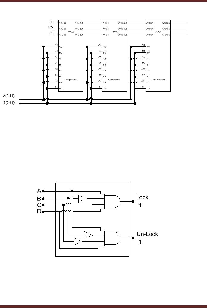
MSI
4-bit Comparator
MSI 74HC85
4-bit Iterative Circuit
based Comparator allows
multiple 74HC85s to be
cascaded
together to form Comparators N x
4-bit Comparators. Three
74HC85s cascaded
together
forms a 12-bit Comparator
circuit. Figure 16.7.
Three
Comparators are cascaded
together. Comparator 1 compares
the least
significant
bits 0 to 3, Comparator 2 compares
bits 4 to 7 and Comparator 3
compares the
most
significant bits 8 to 11.
The respective input bits
are shown connected to the
three
comparators
through thick lines. The
Cascading inputs of Comparator 1
are permanently
connected to
Ground and +5 volts. A<B
in and A>B in are
connected to ground and A=B
in is
connected to +5
Volts. The cascading outputs
of Comparator 1 are connected to
the
respective
cascading inputs of comparator 2.
Similarly, the cascading
outputs of Comparator 1
are
connected to the cascading
inputs of Comparator 3. The
final output of the
12-bit
Comparator
circuit is available at the
cascading outputs of Comparator
3.
156
CS302 -
Digital Logic & Design
Figure
16.7
12-bit
Comparator
Decoders
A Decoder
has multiple inputs and
multiple outputs. The
Decoder device accepts as
an
input a
multi-bit code and activates
one or more of its outputs
to indicate the presence of
the
multi-bit
code. There are different
variations of Decoder
devices.
Basic
Decoder
Consider an
electronic door lock which
unlocks the door when a
4-bit code 1011 is
entered.
The door is locked when
another 4-bit combination
1001 is entered. The lock
and
unlock
circuit is implemented using a
combination of NOT and AND
gates. Figure 16.8
Figure
16.8
Electronic
Door Lock
The
circuit is configured to activate
the Lock output when
the Door Lock code
1011 is
applied at
inputs ABCD. The Un-Lock
output is activated when the
Door Un-Lock code 1001
is
applied at
the inputs ABCD. The
circuit is a Decoder circuit. It
detects the Code 1011
and
activates
the Lock output. Similarly,
it detects the 1001 code
and activates the Un-Lock
output.
Two
different outputs are
activated to indicate the
presence of two unique 4-bit
binary codes.
157
CS302 -
Digital Logic & Design
The
decoder circuit can be
expanded to have more Lock
and Un-Lock outputs to Lock
and Un-
Lock
different doors in a
building.
Applications of
decoders
Decoders
have two major uses in
Computer Systems.
1. Selection of
Peripheral Devices
Computers
have different internal and
external devices like the
Hard Disk, CD Drive,
Modem,
Printer etc. Each of these
different devices is selected by
specifying different codes.
A
decoder
similar to the Electronic
Door Lock/Unlock circuit is
used to uniquely select
or
deselect
the appropriate
devices.
2. Instruction
Decoder
Computer
programs are based on
instructions which are
decode by the
Computer
Hardware
and implemented. The codes
1100010, 1100011, 1110000
and 1000101 represent
Add two
numbers, Subtract two
numbers, Clear the result
and Store the result
instructions.
These
instruction codes are
decoded by an Instruction Decoder to
generate signals that
control
different logic circuits
like the ALU and memory to
perform these
operations.
Binary
Decoder
The
simplest and most commonly
used Decoders are the
n-to-2n Decoders.
These
Decoders
have n inputs and 2n outputs Each, n-bit
input selects 1 out of 2n output code.
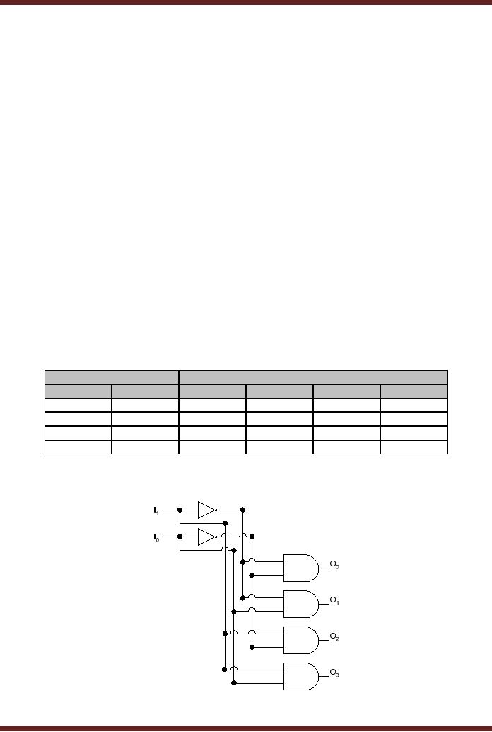
A 2-to-4
Decoder is represented by the
function table. Table16.2.
The 2-to-4 Binary
Decoder
circuit is shown. Figure
16.9
Input
Output
I1
I0
O0
O1
O2
O3
0
0
1
0
0
0
0
1
0
1
0
0
1
0
0
0
1
0
1
1
0
0
0
1
Table
16.2
Function
Table of a 2-to-4 Binary
Decoder
158
CS302 -
Digital Logic & Design
Figure
16.9
2-to-4
Decoder
The 2 to 4
Decoder output O0 is
activated to Logic 1 when
the input is 00. Similarly
for
inputs
01, 10 and 11 the outputs
O1, O2 and
O3 are respectively
activated.
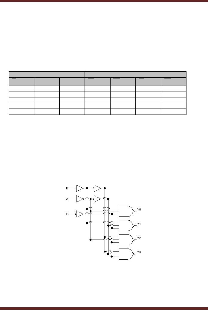
MSI
Decoder
The
74LS139 MSI chip has dual
2-to-4 Decoders. The
function table, table 16.3,
and
the
gatelevel circuit diagram
for the 2-to-4 Decoder is
shown. Figure16.10.The
circuit
diagram is
slightly different form the
one described in figure
16.9.
Input
Output
B
A
Y2
Y1
G
Y3
Y0
1
X
X
1
1
1
1
0
0
0
1
1
1
0
0
0
1
1
1
0
1
0
1
0
1
0
1
1
0
1
1
0
1
1
1
Table
16.3
Function
Table of 74LS139, 2-to-4
Decoder
The
74LS139 has active-low
outputs, thus the output
which is activated is at logic
0
where as
the outputs that ate
are not selected are at
logic 1. A third active-low
input G is the
enable
input, which when set to 0
enables all NAND gates.
Setting the G input to 1
disables all
NAND gates
and all four outputs
are at logic 1 the in-active
state.
Extra
NOT gates are placed at
the inputs A and B. Without
the two extra NOT
gates at
Inputs A
and B, each of the two
inputs present a unit load
of three (a NOT gate and
two NAND
gates). By
having the extra NOT
gates each input presents a
single unit load.
Figure
16.10 74LS139, 2-to-4
Decoder
159
Table of Contents:
- AN OVERVIEW & NUMBER SYSTEMS
- Binary to Decimal to Binary conversion, Binary Arithmetic, 1s & 2s complement
- Range of Numbers and Overflow, Floating-Point, Hexadecimal Numbers
- Octal Numbers, Octal to Binary Decimal to Octal Conversion
- LOGIC GATES: AND Gate, OR Gate, NOT Gate, NAND Gate
- AND OR NAND XOR XNOR Gate Implementation and Applications
- DC Supply Voltage, TTL Logic Levels, Noise Margin, Power Dissipation
- Boolean Addition, Multiplication, Commutative Law, Associative Law, Distributive Law, Demorgans Theorems
- Simplification of Boolean Expression, Standard POS form, Minterms and Maxterms
- KARNAUGH MAP, Mapping a non-standard SOP Expression
- Converting between POS and SOP using the K-map
- COMPARATOR: Quine-McCluskey Simplification Method
- ODD-PRIME NUMBER DETECTOR, Combinational Circuit Implementation
- IMPLEMENTATION OF AN ODD-PARITY GENERATOR CIRCUIT
- BCD ADDER: 2-digit BCD Adder, A 4-bit Adder Subtracter Unit
- 16-BIT ALU, MSI 4-bit Comparator, Decoders
- BCD to 7-Segment Decoder, Decimal-to-BCD Encoder
- 2-INPUT 4-BIT MULTIPLEXER, 8, 16-Input Multiplexer, Logic Function Generator
- Applications of Demultiplexer, PROM, PLA, PAL, GAL
- OLMC Combinational Mode, Tri-State Buffers, The GAL16V8, Introduction to ABEL
- OLMC for GAL16V8, Tri-state Buffer and OLMC output pin
- Implementation of Quad MUX, Latches and Flip-Flops
- APPLICATION OF S-R LATCH, Edge-Triggered D Flip-Flop, J-K Flip-flop
- Data Storage using D-flip-flop, Synchronizing Asynchronous inputs using D flip-flop
- Dual Positive-Edge triggered D flip-flop, J-K flip-flop, Master-Slave Flip-Flops
- THE 555 TIMER: Race Conditions, Asynchronous, Ripple Counters
- Down Counter with truncated sequence, 4-bit Synchronous Decade Counter
- Mod-n Synchronous Counter, Cascading Counters, Up-Down Counter
- Integrated Circuit Up Down Decade Counter Design and Applications
- DIGITAL CLOCK: Clocked Synchronous State Machines
- NEXT-STATE TABLE: Flip-flop Transition Table, Karnaugh Maps
- D FLIP-FLOP BASED IMPLEMENTATION
- Moore Machine State Diagram, Mealy Machine State Diagram, Karnaugh Maps
- SHIFT REGISTERS: Serial In/Shift Left,Right/Serial Out Operation
- APPLICATIONS OF SHIFT REGISTERS: Serial-to-Parallel Converter
- Elevator Control System: Elevator State Diagram, State Table, Input and Output Signals, Input Latches
- Traffic Signal Control System: Switching of Traffic Lights, Inputs and Outputs, State Machine
- Traffic Signal Control System: EQUATION DEFINITION
- Memory Organization, Capacity, Density, Signals and Basic Operations, Read, Write, Address, data Signals
- Memory Read, Write Cycle, Synchronous Burst SRAM, Dynamic RAM
- Burst, Distributed Refresh, Types of DRAMs, ROM Read-Only Memory, Mask ROM
- First In-First Out (FIFO) Memory
- LAST IN-FIRST OUT (LIFO) MEMORY
- THE LOGIC BLOCK: Analogue to Digital Conversion, Logic Element, Look-Up Table
- SUCCESSIVE APPROXIMATION ANALOGUE TO DIGITAL CONVERTER