 |
OLMC for GAL16V8, Tri-state Buffer and OLMC output pin |
| << OLMC Combinational Mode, Tri-State Buffers, The GAL16V8, Introduction to ABEL |
| Implementation of Quad MUX, Latches and Flip-Flops >> |

CS302 -
Digital Logic & Design
Lesson
No. 21
THE
GAL16V8
This
device has eight inputs,
two special function input
pins and eight pins
that can be
used as
inputs or output. The
architecture of the GAL16V8 is
similar to that of a PAL and
it is
designed to be
programmed in one of the
three available modes to
emulate most of the
existing
PALs, thus replacing the
PAL. The three modes in
which PALs are programmed
are
� Simple
� Complex
� Registered
The
simple and complex modes
are associated with the
Combinational Logic whereas
the
Registered
mode is associated with
Sequential Logic.
The
GAL16V8 has eight OLMCs
each connected to eight
product terms. Each
product
term is
implemented using a 32-bit
input AND gate. The 32
inputs comprise of the
16
complemented
and un-complemented inputs of
the 8 input pins and 16
complemented and un-
complemented
inputs of the 8 input/output
pins that can be configured
as input pins.
OLMC
for GAL16V8
The
OLMC of the GAL16V8 is
similar to the OLMC of the
GAL22V10 with some
enhancements.
The main aspects of the
GAL16V8 OLMC are
Tri-state
Buffer and OLMC output
pin
The
tri-state buffer connecting
the output of the OLMC
circuit to the output pin
is
controlled
through four different
sources. The tri-state
buffer control input can be
connected in
four
different ways.
1. Connected to
Vcc. The output is
always enabled.
2. Connected to
GND. The output is disabled
and the output pin is
configured as an input
pin.
3. Connected to
the external pin (11)
which can be connected to Vcc or GND. The
tri-state
buffer is
therefore controlled externally by
applying an appropriate signal at
the pin.
4. Connected to
the output of one of the
eight AND gates connected to
the OLMC. Thus
the
tri-state
buffer is controlled by a logical
expression.
The
feedback from the OLMC to
the AND Gate array
input
The
OLMC can be configured to
provide a feedback input
signal to the AND gate
array
input.
There are three
possibilities.
1. Connecting
the feedback signal line to
the output of the OLMC.
This allows the output
of
the
OLMC to be connected back to
the AND gate array input.
This allows
implementation
of Sequential
Logic circuits.
2. Connecting
the feedback signal line to
the output of the adjacent
OLMC. This also
allows
implementation
of Sequential Logic
circuits.
3. Connecting
the feedback signal line to
a flip-flop. This allows
implementation of
synchronized
Sequential circuits.
The
output of the Sum of Product
term
The OR
gate used to implement the
Sum-of-Product term has its
output connected to
the
output pin thorough the
tri-state buffer. The
tri-state buffer is also
connected to the
output
from
the flip-flop. Thus either
of the two inputs to the
tri-state buffer can be
selected. The
output of
the OR gate can also be
programmed for output
polarity by configuring the
XOR gate
connected at
the output of the OR
gate.
207
CS302 -
Digital Logic & Design
Simple
Mode
In the
Simple Mode the OLMC is
configured as dedicated active
combinational output
or as dedicated
input (limited to six).
Three possible combinations of
the Simple Mode are
� Combinational
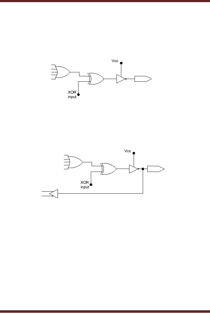
Output. Figure 21.1
� Combinational
Output with feedback to AND
Array. Fig 21.2
� Dedicated
input. Fig 21.3
Figure
21.1
Combinational
Output
In the
Combinational Output the
OLMC is configured to give an
output which is
either
active-low or
active-high. The active-state of
the output is determined by
the XOR input.
The
tri-state
buffer control pin is set to
logic high by connecting it to
Vcc. The
Sum-of-Product term
generated by
the OR gate has eight
product terms.
Figure
21.2
Combinational
Output with feedback to AND
array
The
Combinational Output with
feedback to AND array is similar.
The tri-state control
pin is
set to logic high (Vcc), the XOR gate
input determines the
active-state of the output.
The
signal at
the output is also connected
to the input of the AND
array through the buffer
which
provides
inverting and non-inverting
outputs. The feedback
capability is limited to six
OLMCs
as they
have a physical connection
from the tri-state buffer
output to the AND gate array
input.
OLMCs
connected to input/output pins 15
and 16 do not have the
feedback path
therefore
they
can not be programmed with
Combinational output with
feedback.
208
CS302 -
Digital Logic & Design
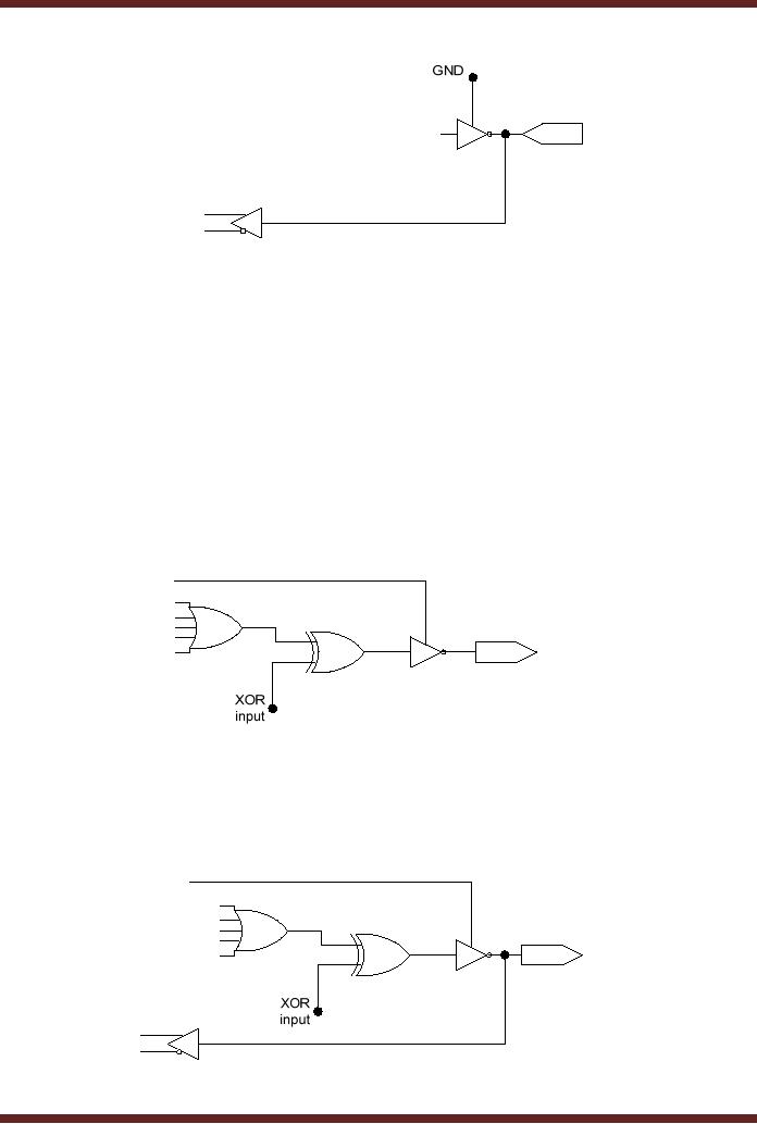
Figure
21.3
Dedicated
Input
In the
Dedicated Input configuration
the tri-state buffer is
configured in the
high
impedance
state by setting the control
pin of the tri-state buffer
to low (GND). Thus the
output
pin is
connected to an input signal
which is passed to the input
of the AND Array in
its
complemented
and un-complemented form by
the buffer.
Complex
Mode
In this
mode the OLMCs can be
configured in two ways. In
the complex Mode the
tri-
state
control is formed by a logical
expression, this leaves
seven product terms that
can be
used to
form a sum-of product
expression. Two possible
combinations of the Complex
Mode
are
� Combinational
Output. Fig. 21.4
� Combinational
Input/Output. Fig.
21.5
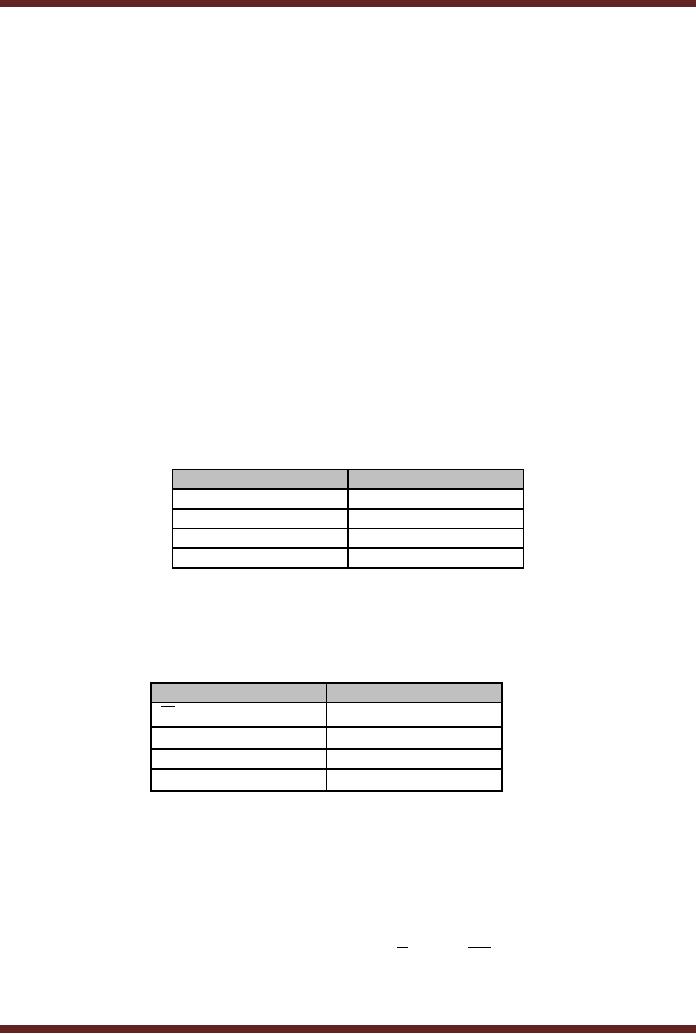
Figure
21.4
Combinational
Output
The
tri-sate buffer is enabled by
connecting the control input
of the buffer to the
output
of one of
the AND gate. Thus the
tri-state buffer is controlled by
programming a product
term.
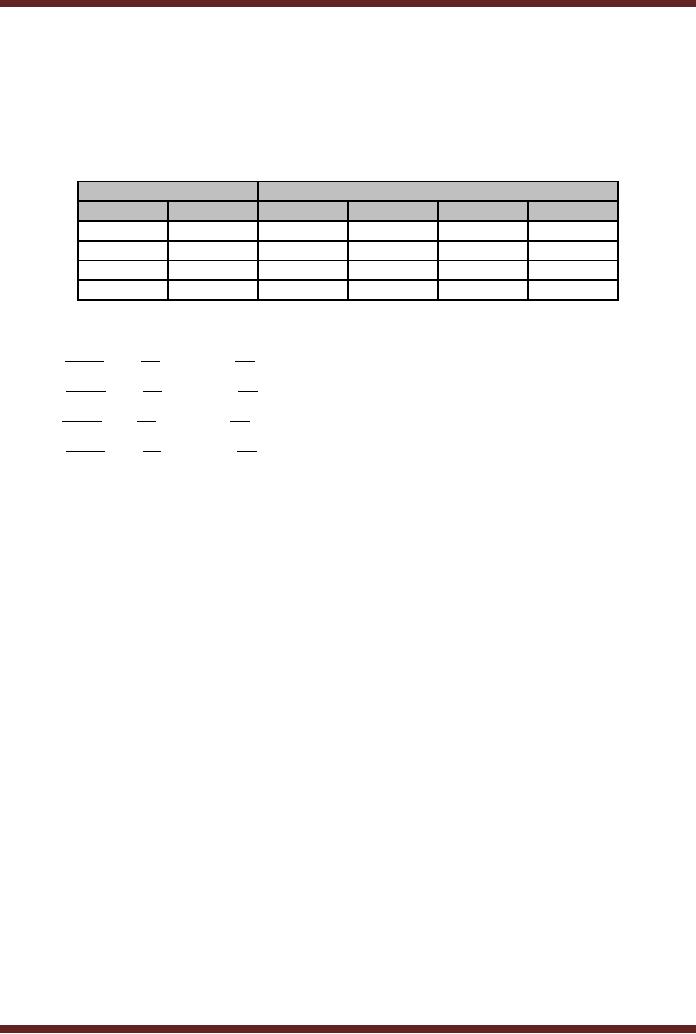
Similarly,
the Combinational Input/Output
Mode is also implemented by
connecting the
tri-state
buffer
control input to the output
of the AND gate. OLMCs which
have the feedback
path
connecting
the output to the input of
the AND gate array can be
used in this mode.
Figure
21.5
Combinational
Input/Output
209
CS302 -
Digital Logic & Design
Introduction to
ABEL
ABEL
which is an acronym for
Advanced Boolean Expression
Language is a hardware
description
language used for
implementing logic designs
using PLDs. ABEL is a
device-
independent
language and can be used to
program any type of PLD.
ABEL is run on a
computer
connected to a PLD programmer
which programs the
PLD.
ABEL
provides three different
text-based methods for
describing and entering a
logic
design.
The three methods
are
� Boolean
Equations
� Truth
Tables
� State
Diagrams
The
Boolean Equations and the
Truth Table method are
used for Combinational
Logic
Circuits.
The State Diagram is used
specifically for Sequential
Logic circuits. The
Boolean
Equations
and the Truth Table
method can also be used
for describing and
entering
Sequential
Logic Circuits.
Boolean
Operations and Boolean
Notations
The
NOT, AND, OR and XOR
operations have special
symbols in ABEL as shown
in
table
21.1
Logic
Operation
ABEL
Symbol
NOT
!
AND
&
OR
#
XOR
$
Table
21.1
ABEL
Symbols for logic
operations
The
standard Boolean notations in
terms of ABEL notations are
defined in table
20.2.
The
operators !, &, # and $ have
precedence in the order
given in table.
Boolean
Notation
ABEL
Notation
!A
A
A.B
A&B
A +B
A#B
A ⊕B
A$B
Table
21.2
Boolean
and equivalent ABEL
Notations
3. Boolean
Equations
One of
the ABEL entry methods
uses logic equations. In
ABEL any letter or
combination of
letters and numbers can be
used to identify variables.
ABEL however is case-
sensitive,
thus variable `A' is treated
separately from variable
`a'. All ABEL equations
must end
with
`;'. Figure 21.6
Boolean
expression F
=
AB + AC + BD
ABEL
expression F = A & !B # A & C # !B &
!D;
Figure
21.6
ABEL
representation of Boolean
expression
210
CS302 -
Digital Logic & Design
Multiple
Inputs and
Outputs
In some
cases, multiple input and
output variables can be
grouped as a set to
simplify
an equation.
Fig 21.7. Thus D0, D1 and D2 input or output variables
can be defined by a
single
variable D
using the ABEL notation D =
[D0, D1, D2];
A 4-input
4-bit Multiplexer is represented by
the function table 21.3.
The Boolean
expressions
representing the operation of
the MUX are shown in figure
21.7.
Select
Inputs
Outputs
S1
S0
Y3
Y2
Y1
Y0
0
0
A3
A2
A1
A0
0
1
B3
B2
B1
B0
1
0
C3
C2
C1
C0
1
1
D3
D2
D1
D0
Table
21.3
Truth
Table of 4-input 4-bit
MUX
Y3 = A 3 S1 S 0 + B3 S1S 0 + C3S1 S 0 + D3S1S 0
Y2 = A 2 S1 S 0 + B 2 S1S 0 + C 2S1 S 0 + D 2S1S 0
Y1 = A 1 S1 S 0 + B1 S1S 0 + C1S1 S 0 + D1S1S 0
Y0 = A 0 S1 S 0 + B 0 S1S 0 + C 0S1 S 0 + D 0S1S 0
Figure
21.7 Boolean expressions
representing a 4-input 4-bit
MUX
The
ABEL notations representing
the operation of the MUX are
shown in figure 21.8.
Y3 = A3 &
!S1 & !S0 # B3 & !S1 & S0 #
C3 & S1 & !S0 # D3 & S1 &
S0;
Y2 = A2 &
!S1 & !S0 # B2 & !S1 & S0 #
C2 & S1 & !S0 # D2 & S1 &
S0;
Y1 = A1 &
!S1 & !S0 # B1 & !S1 & S0 #
C1 & S1 & !S0 # D1 & S1 &
S0;
Y0 = A0 &
!S1 & !S0 # B0 & !S1 & S0 #
C0 & S1 & !S0 # D0 & S1 &
S0;
Figure
21.8
ABEL
notations representing a 4-input
4-bit MUX
The
four ABEL notations can be
represented by a single notation if
variables A3, A2, A1
and
A0 are
defined as a set A. Similarly,
sets B, C and D can be
defined. Figure 21.9
A = [A3,
A2, A1, A0];
B = [B3,
B2, B1, B0];
C = [C3,
C2, C1, C0];
D = [D3,
D2, D1, D0];
Y = [Y3,
Y2, Y1, Y0];
S = [S1,
S0];
The
ABEL notation representing
the MUX is
Y = (S = = 0) & A # (S =
= 1) & B # (S = = 2) & C # (S = = 3) & D;
The `= =' is a
relational operator
Figure
21.9
ABEL
representation of multiple inputs
and outputs
211

CS302 -
Digital Logic & Design
4. Truth
Table
ABEL
accepts a logical design
described in the form of a
Truth Table. Truth Tables
are
sometimes
more convenient in describing
certain logic circuits. The
ABEL Truth Table
format
includes a
header and the truth
table entries.
TRUTH_TABLE
( [ A, B, C, D] → [ X1,
X2])
A, B, C and D
are the inputs and XI
and X2 are the
outputs.
The
truth table of an XOR gate
is represented by the ABEL
Truth Table notation. Figure
21.10.
TRUTH_TABLE
( [A, B]
→ [X])
[0, 0]
→ [0];
[0, 1]
→ [1];
[1, 0]
→ [1];
[1, 1]
→ [0];
Figure
21.10 ABEL representation of
the Truth table of an XOR
gate
The
2-bit Comparator logic
circuit can be described in
terms of the truth table
using ABEL
notations.
Fig 21.11
TRUTH_TABLE
( [A1,
A0, B1, B0] → [G, E, L]
)
[0, 0, 0, 0]
→ [0, 1,
0];
[0, 0, 0, 1]
→ [0, 0,
1];
[0, 0, 1, 0]
→ [0, 0,
1];
[0, 0, 1, 1]
→ [0, 0,
1];
[0, 1, 0, 0]
→ [1, 0,
0];
[0, 1, 0, 1]
→ [0, 1,
0];
[0, 1, 1, 0]
→ [0, 0,
1];
[0, 1, 1, 1]
→ [0, 0,
1];
[1, 0, 0, 0]
→ [1, 0,
0];
[1, 0, 0, 1]
→ [1, 0,
0];
[1, 0, 1, 0]
→ [0, 1,
0];
[1, 0, 1, 1]
→ [0, 0,
1];
[1, 1, 0, 0]
→ [1, 0,
0];
[1, 1, 0, 1]
→ [1, 0,
0];
[1, 1, 1, 0]
→ [1, 0,
0];
[1, 1, 1, 1]
→ [0, 1,
0];
Figure
21.11 ABEL representation of
the Truth table of a 2-bit
Comparator
The
ABEL notation can be
rewritten by defining a set.
Fig 21.12
INPUT =
[A1, A0, B1,
B0];
TRUTH_TABLE
( INPUT
→ [G, E, L]
)
0 → [0, 1,
0];
1 → [0, 0,
1];
2 → [0, 0,
1];
3 → [0, 0,
1];
212

CS302 -
Digital Logic & Design
4 → [1, 0,
0];
5 → [0, 1,
0];
6 → [0, 0,
1];
7 → [0, 0,
1];
8 → [1, 0,
0];
9 → [1, 0,
0];
10 → [0, 1,
0];
11 → [0, 0,
1];
12 → [1, 0,
0];
13 → [1, 0,
0];
14 → [1, 0,
0];
15 → [0, 1,
0];
Figure
21.12 ABEL representation of a
Truth Table of a 2-bit
Comparator using a
set
Test
Vectors
Once
the Logic circuit design
has been entered its
operation is verified by using
`test
vectors'. A
`test vector' specifies the
inputs and the corresponding
outputs. The software
simulates
the operation of the logic
circuit by applying the test
vector and checking
the
outputs.
Test vectors are essentially
the same as Truth Tables.
Figure 21.13
TEST_VECTORS
( [A1,
A0, B1, B0] → [G, E, L]
)
[0, 0, 0, 0]
→ [0, 1,
0];
[0, 0, 0, 1]
→ [0, 0,
1];
[0, 0, 1, 0]
→ [0, 0,
1];
[0, 0, 1, 1]
→ [0, 0,
1];
[0, 1, 0, 0]
→ [1, 0,
0];
[0, 1, 0, 1]
→ [0, 1,
0];
[0, 1, 1, 0]
→ [0, 0,
1];
[0, 1, 1, 1]
→ [0, 0,
1];
[1, 0, 0, 0]
→ [1, 0,
0];
[1, 0, 0, 1]
→ [1, 0,
0];
[1, 0, 1, 0]
→ [0, 1,
0];
[1, 0, 1, 1]
→ [0, 0,
1];
[1, 1, 0, 0]
→ [1, 0,
0];
[1, 1, 0, 1]
→ [1, 0,
0];
[1, 1, 1, 0]
→ [1, 0,
0];
[1, 1, 1, 1]
→ [0, 1,
0];
Figure
21.13 Test Vector of a 2-bit
Comparator
INPUT =
[A1, A0, B1,
B0];
TEST_VECTORS
( INPUT → [G, E, L]
)
0 → [0, 1,
0];
1 → [0, 0,
1];
2 → [0, 0,
1];
3 → [0, 0,
1];
4 → [1, 0,
0];
5 → [0, 1,
0];
6 → [0, 0,
1];
7 → [0, 0,
1];
213

CS302 -
Digital Logic & Design
8 → [1, 0,
0];
9 → [1, 0,
0];
10 → [0, 1,
0];
11 → [0, 0,
1];
12 → [1, 0,
0];
13 → [1, 0,
0];
14 → [1, 0,
0];
15 → [0, 1,
0];
Figure
21.14
Test
Vector of a 2-bit Comparator
using a set
The
ABEL Input File
When an
Input (source) file is
created in ABEL a module is
created which has
three
sections.
The three sections
are
4.
Declarations
The
declaration section generally
includes the device
declaration, pin declarations
and
set
declarations. Figure 21.15.
Device declaration is used to
specify the PLD device
that is to
be programmed.
The device is referred to as
the target device.
Decoder
device `P22V10';
A0,
A1, A2, A3, PIN 1, 2, 3,
4;
INPUT =
[A1, A0, B1,
B0];
Figure
21.15 ABEL Input
declarations
The
`Decoder' is a description which
can be anything defined by
the user
The
`device' is a reserved keyword
which can be in lower or
upper case.
The
`P22V10' is the device name.
It should be in the format
shown.
`PIN" is a
keyword which can be in
lower or upper case.
Pin
declaration defines the
relationship between the
variables and the
corresponding pin
numbers of
the PLD.
`INPUT'
defines a set made up of set
elements A1, A0, B1 and
B0. In subsequent
ABEL
notations
the set `INPUT' can be
used instead of set
variables.
5. Logic
Descriptions
Logic
descriptions include the
three methods of describing a
logic circuit. Two
methods
the
Boolean equation and the
Truth Table method already
have been discussed.
6. Test
Vectors
The
Test Vector format has
been described. The Test
vector description is used
to
simulate
the logic circuit and
verify its operation.
214

CS302 -
Digital Logic & Design
The
Documentation file
After an
input file is processed by
ABEL a documentation file is
generated which
provides a
hardcopy of the final
reduced equations, a JEDEC
file and a device pin
diagram.
The
JEDEC file
The
JEDEC file is downloaded to
the PLD programmer to
program the appropriate
PLD
device.
215
Table of Contents:
- AN OVERVIEW & NUMBER SYSTEMS
- Binary to Decimal to Binary conversion, Binary Arithmetic, 1’s & 2’s complement
- Range of Numbers and Overflow, Floating-Point, Hexadecimal Numbers
- Octal Numbers, Octal to Binary Decimal to Octal Conversion
- LOGIC GATES: AND Gate, OR Gate, NOT Gate, NAND Gate
- AND OR NAND XOR XNOR Gate Implementation and Applications
- DC Supply Voltage, TTL Logic Levels, Noise Margin, Power Dissipation
- Boolean Addition, Multiplication, Commutative Law, Associative Law, Distributive Law, Demorgan’s Theorems
- Simplification of Boolean Expression, Standard POS form, Minterms and Maxterms
- KARNAUGH MAP, Mapping a non-standard SOP Expression
- Converting between POS and SOP using the K-map
- COMPARATOR: Quine-McCluskey Simplification Method
- ODD-PRIME NUMBER DETECTOR, Combinational Circuit Implementation
- IMPLEMENTATION OF AN ODD-PARITY GENERATOR CIRCUIT
- BCD ADDER: 2-digit BCD Adder, A 4-bit Adder Subtracter Unit
- 16-BIT ALU, MSI 4-bit Comparator, Decoders
- BCD to 7-Segment Decoder, Decimal-to-BCD Encoder
- 2-INPUT 4-BIT MULTIPLEXER, 8, 16-Input Multiplexer, Logic Function Generator
- Applications of Demultiplexer, PROM, PLA, PAL, GAL
- OLMC Combinational Mode, Tri-State Buffers, The GAL16V8, Introduction to ABEL
- OLMC for GAL16V8, Tri-state Buffer and OLMC output pin
- Implementation of Quad MUX, Latches and Flip-Flops
- APPLICATION OF S-R LATCH, Edge-Triggered D Flip-Flop, J-K Flip-flop
- Data Storage using D-flip-flop, Synchronizing Asynchronous inputs using D flip-flop
- Dual Positive-Edge triggered D flip-flop, J-K flip-flop, Master-Slave Flip-Flops
- THE 555 TIMER: Race Conditions, Asynchronous, Ripple Counters
- Down Counter with truncated sequence, 4-bit Synchronous Decade Counter
- Mod-n Synchronous Counter, Cascading Counters, Up-Down Counter
- Integrated Circuit Up Down Decade Counter Design and Applications
- DIGITAL CLOCK: Clocked Synchronous State Machines
- NEXT-STATE TABLE: Flip-flop Transition Table, Karnaugh Maps
- D FLIP-FLOP BASED IMPLEMENTATION
- Moore Machine State Diagram, Mealy Machine State Diagram, Karnaugh Maps
- SHIFT REGISTERS: Serial In/Shift Left,Right/Serial Out Operation
- APPLICATIONS OF SHIFT REGISTERS: Serial-to-Parallel Converter
- Elevator Control System: Elevator State Diagram, State Table, Input and Output Signals, Input Latches
- Traffic Signal Control System: Switching of Traffic Lights, Inputs and Outputs, State Machine
- Traffic Signal Control System: EQUATION DEFINITION
- Memory Organization, Capacity, Density, Signals and Basic Operations, Read, Write, Address, data Signals
- Memory Read, Write Cycle, Synchronous Burst SRAM, Dynamic RAM
- Burst, Distributed Refresh, Types of DRAMs, ROM Read-Only Memory, Mask ROM
- First In-First Out (FIFO) Memory
- LAST IN-FIRST OUT (LIFO) MEMORY
- THE LOGIC BLOCK: Analogue to Digital Conversion, Logic Element, Look-Up Table
- SUCCESSIVE –APPROXIMATION ANALOGUE TO DIGITAL CONVERTER