 |
IMPLEMENTATION OF AN ODD-PARITY GENERATOR CIRCUIT |
| << ODD-PRIME NUMBER DETECTOR, Combinational Circuit Implementation |
| BCD ADDER: 2-digit BCD Adder, A 4-bit Adder Subtracter Unit >> |
CS302 -
Digital Logic & Design
Lesson
No. 14
IMPLEMENTATION OF
AN ODD-PARITY GENERATOR
CIRCUIT
The
first step in implementing
any circuit is to represent
its operation in terms of a
Truth
or Function
table. The function table
for an 8-bit data as input
has 28 has 256
input
combinations,
which becomes unmanageable.
Therefore, for the sake of
simplicity a 4-bit
data
with
odd parity is assumed. The
receiver circuit is also
based on the 4-bit data.
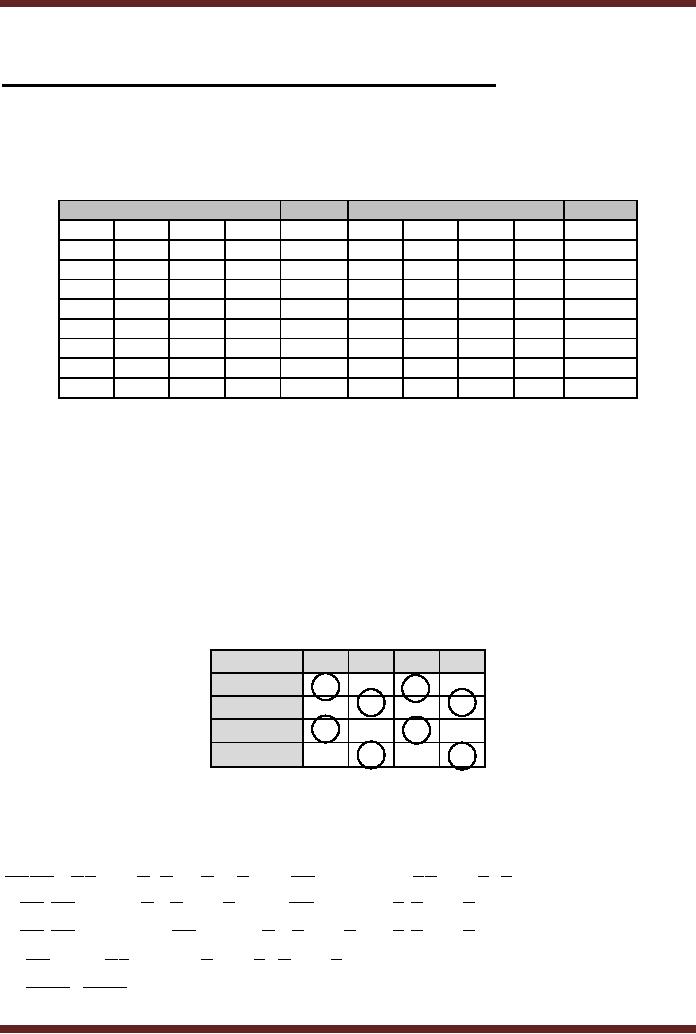
The function
table
for the 4-bit data is
shown. Figure 14.1
Input
Output
Input
Output
D3
D2
D1
D0
P
D3
D2
D1
D0
P
0
0
0
0
1
1
0
0
0
0
0
0
0
1
0
1
0
0
1
1
0
0
1
0
0
1
0
1
0
1
0
0
1
1
1
1
0
1
1
0
0
1
0
0
0
1
1
0
0
1
0
1
0
1
1
1
1
0
1
0
0
1
1
0
1
1
1
1
0
0
0
1
1
1
0
1
1
1
1
1
Table
14.1
Function
Table of an Odd-Parity Generator
Circuit
The
function table represents
the 16 possible combinations of 4
data bits. The 4
data
bits
are represented by variables
D3, D2, D1 and D0.
The output P represents the
state of the
Parity
bit. Since Odd-Parity is
being used therefore the
4-bit data and the
parity bit should
add
up to give
odd number of 1s. The
function table shows the
Parity bit set to 1 when
the 16, 4-bit
data
input combinations have no 1s or an
even number of 1s.
The
information in the function
table is mapped directly to a
four variable K-map
to
simplify
the Boolean expression
represented by the Odd-Parity
generator function. None of
the
1s mapped in
the K-map are adjacent to
each other thus the
function mapped to the
K-map
can
not be simplified. Figure
14.1
D3D2\D1D0
00
01
11
10
1
0
1
0
00
0
0
01
1
1
11
1
0
1
0
1
1
10
0
0
Figure
14.1
Karnaugh
map of the Odd-Parity
Generator Function
However,
using the Rules of Boolean
algebra, applying Demorgan's
theorems and
knowing
the function table of XOR
and XNOR gates the
Boolean expression can be
simplified.
Simplifying
the expression based on SOP
form results in
ABCD + ABCD + ABCD + ABCD + ABCD + ABCD
+
ABCD
+
ABCD
= AB(CD + CD) + AB(CD + CD) + AB(CD + CD) + AB(CD + CD)
= AB(CD + CD) + AB(CD + CD) + AB(CD + CD) + AB(CD + CD)
= (CD + CD)(AB + AB) + (CD + CD)(AB + AB)
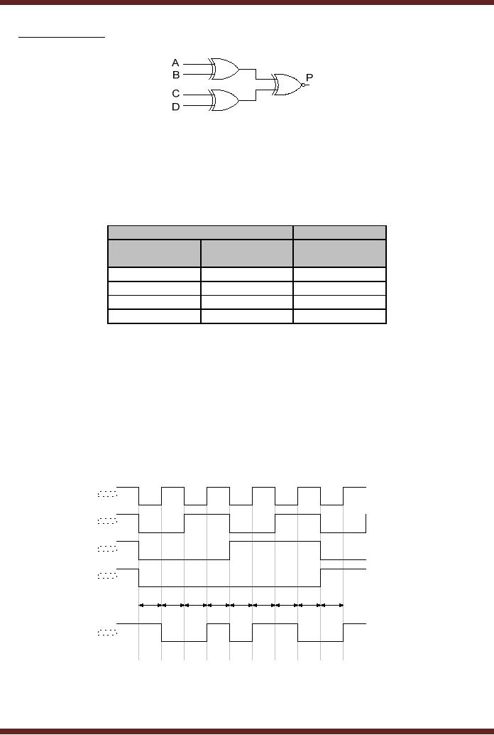
= (C ⊕ D)(A ⊕ B) + (C ⊕ D)(A ⊕ B)
131
CS302 -
Digital Logic & Design
= (A ⊕ B) ⊕ (C ⊕ D)
Figure
14.2
Odd-Parity
Generator Circuit
The
parity generator circuit
shown checks the 4-bit
number, generates a parity
bit
which
along with the 4-bit
data is transmitted. The
receiver calculates the
parity bit of the
received
4-bit data and compares it
with the parity sent. If
the received and calculated
parity
bits
are the same, then no
error has occurred. An XOR
gate is used to detect
parity errors.
Table
14.2
Input
Output
Received
Calculated
Error
Output
Parity
Bit
Parity
Bit
0
0
0
0
1
1
1
0
1
1
1
0
Table
14.2
Detecting
Error at Receiver End
Operation of
Odd-Parity Generator
Circuit
The
timing diagram shows the
operation of the Odd-Parity
generator circuit.
Figure
14.3.
The A, B, C and D timing
diagrams represent the
changing 4-bit data values.
During time
interval t0
the 4-bit data value is
0000, during time interval
t1, the data value
changes to 0001.
Similarly
during time intervals t2,
t3, t4 up to t8 the data
values change to 0010, 0011,
0100
and
1000 respectively. During
interval t0 the output of
the two XOR gates is 0
and 0, therefore
the
output of the XNOR gate is
1. At interval t1, the
outputs of the two XOR
gates is 1 and 0,
therefore
the output of the XNOR
gate is 0. The output P can
similarly be traced for
intervals t2
to
t8.
D
C
B
A
t0
t1
t2
t3
t4
t5
t6
t7
t8
P
Figure
14.3
Timing
Diagram of Odd-Parity Generator
Circuit
132
CS302 -
Digital Logic & Design
XOR
and XNOR Gates
XOR
and XNOR gates are
used to implement the
Odd-Parity Generator Circuit.
An
XNOR is
also used to check for
single bit errors at the
Receiver end. Both, the
XOR and
XNOR
gates perform simple
comparison functions. The
XOR gate detects dissimilar
inputs,
where as
the XNOR gate looks
for similar inputs. Both,
the gates can be considered
as
functional
devices as each gate
performs a simple specific
function.
The
XOR and XNOR gates
are implemented using a
combination of NOT, AND
and
OR gates.
Since the function performed
by the XOR and XNOR
gate is commonly used
in
digital
circuits therefore XOR and
XNOR gates are available in
Integrated circuit form
which
can be
readily used instead of
implementing an XOR and XNOR
circuit based on
NOT-AND-
OR combination
of gates.
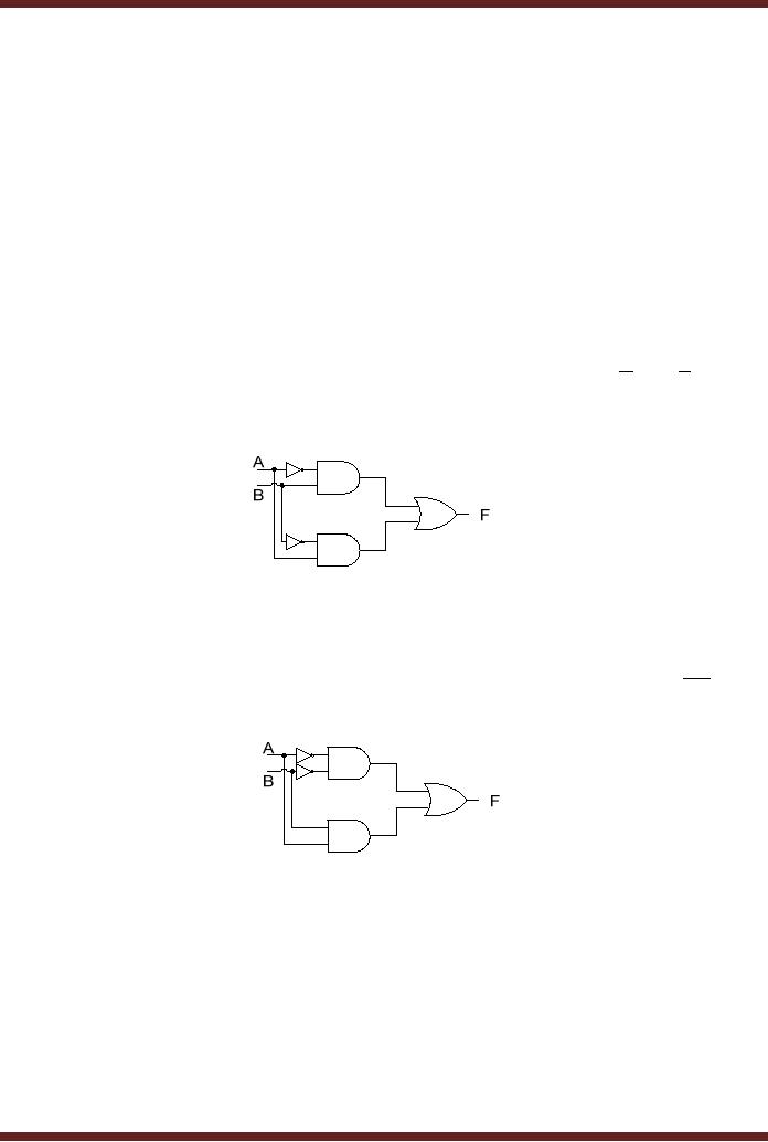
The
function table for the
Parity Error detector
circuit is identical to the
truth table of an
XOR
gate. Boolean expression
representing the function of an
XOR gate is AB + AB which is
implemented
using a combination NOT, AND
and OR gates.
Figure
14.3
Implementation
of XOR Gate
The
XNOR gate is also
implemented using a combination of
NOT, AND and OR
gates.
The
function of the XNOR gate is
represented in term of Boolean
expression as AB
+
AB .
Figure
14.4
Figure
14.4
Implementation
of XNOR Gate
Combinational
Function Devices
Digital
circuits are formed by the
combination of Logic Gates.
Most Combinational
circuits
perform standard and useful
functions such as addition,
comparison, decoding
and
encoding,
multiplexing and de-multiplexing,
selection and enabling of
devices and many
more
operations.
Implementation of these standard
functional devices through
combination of gates
takes up
considerable space, therefore
these functional devices are
implemented as MSI or
Medium
Scale Integrated
Chips.
133
CS302 -
Digital Logic & Design
The
simplest of these functional
devices can be considered to be
the NAND and NOR
gates
which perform the AND-NOT
and OR-NOT functions. The
XOR and XNOR Gates
are
also a
combination of NOT-AND-OR gates
which perform functions to
detect dissimilar and
similar
inputs.
Half
Adder and Full
Adder
A single
bit binary adder circuit
basically adds two bits
and a carry bit, generated
by the
addition of
the least significant bits.
The output of the single
bit adder circuit generates
a sum
bit
and a carry bit. A single
digit binary adder circuit
therefore has three inputs,
one
representing
single bit number A, the
other representing the
single bit number B and
the third
bit
represents the single bit
carry. The single bit
binary adder has two
bit output. One
bit
represents
the Sum between numbers A
and B. The other bit
represents the carry
bit
generated
due to addition.
In Digital
logic terminology the adder
which has been described is
known as a full
adder. An
adder circuit that only
has two bit input
representing the two single
bit numbers A
and B
and does not have
the carry bit input
from the least significant
digit is regarded as a
half-adder.
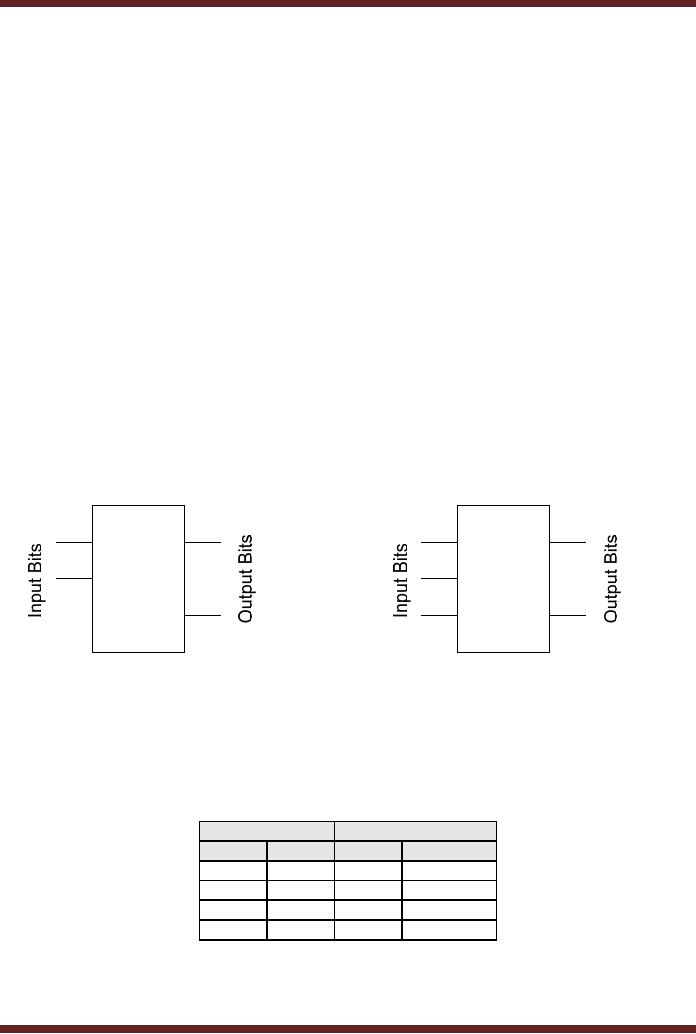
The block diagrams represent
a Half-Adder and a Full-Adder.
Figure 14.5.
1.
Half-Adder
A Half-Adder
can be fully described in
terms of its Function table,
its Sum and
Carry
Out
Boolean Expressions and the
circuit Implementation.
∑
∑
∑
∑
A
A
B
B
Cout
Cout
Cin
Half-Adder
Full-Adder
Figure
14.5
Block
diagrams of Half-Adder and
Full-Adder
Half-Adder
Function Table
The
Half-Adder has a 2-bit input
and a 2-bit output. The
function table of the
Half-Adder
has
two input columns
representing the two single
bit numbers A and B. The
function table
also
has two output columns
representing the Sum bit
and Carry Out bit.
Table 14.3
Input
Output
A
B
Sum
Carry
Out
0
0
0
0
0
1
1
0
1
0
1
0
1
1
0
1
Table
14.3
Half-Adder
Function Table
134
CS302 -
Digital Logic & Design
Half-Adder Sum
& Carry Out Boolean
Expressions
The
Sum and Carry Out
expressions of the Half-Adder
can be determined from
the
function
table. The Half-Adder Sum
and Carry Out outputs
are defined by the
expressions
Sum = AB + AB = A ⊕ B
CarryOut
=
AB
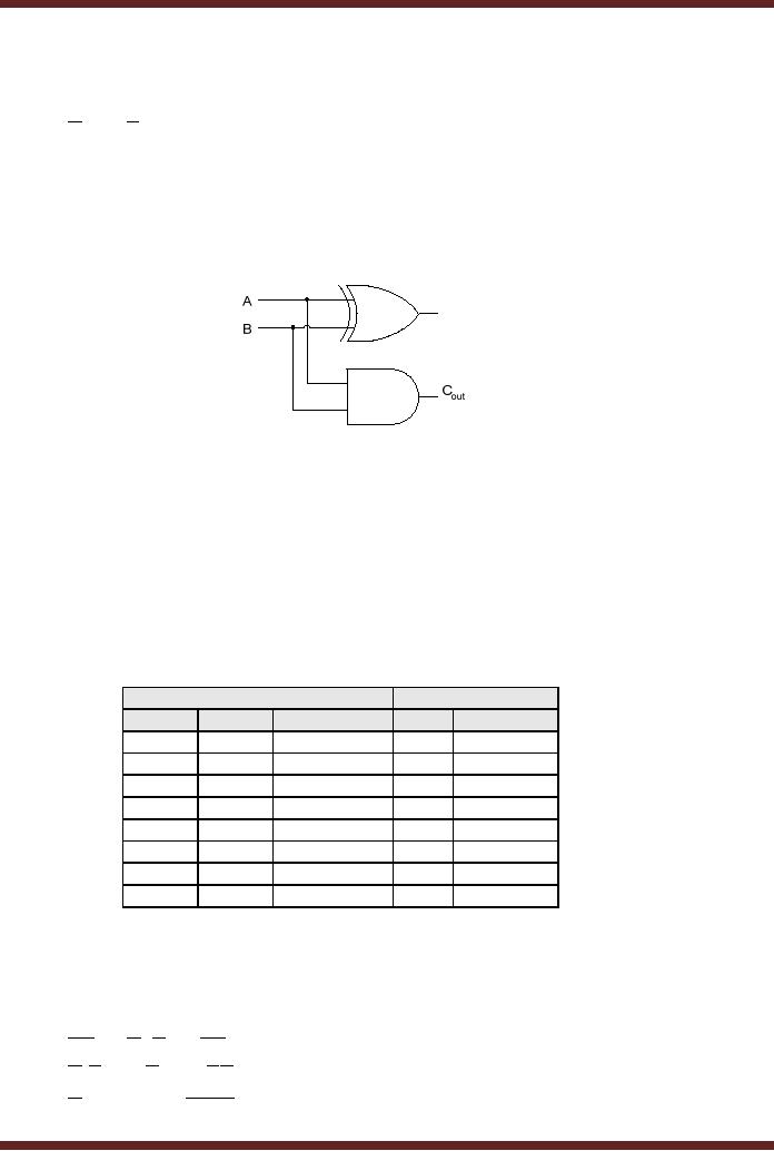
Half-Adder
Logic Circuit
The
Half-Adder Logic Circuit can
be directly implemented from
the Sum and Carry
Out
Boolean
expressions. Figure
14.6
∑
Figure
14.6
Half-Adder
Logic Circuit
2.
Full-Adder
A Full-Adder
can be fully described in
terms of its Function table,
its Sum and
Carry
Out
Boolean Expressions and the
circuit Implementation.
Full-Adder
Function Table
The
Full-Adder has a 3-bit input
and a 2-bit output. The
function table of the
Full-Adder
has
three input columns
representing the two single
bit numbers A, B and the
Carry In bit. The
function
table also has two
output columns representing
the Sum bit and
Carry Out bit.
Table
14.4
Input
Output
A
B
Carry
In(C)
Sum
Carry Out
0
0
0
0
0
0
0
1
1
0
0
1
0
1
0
0
1
1
0
1
1
0
0
1
0
1
0
1
0
1
1
1
0
0
1
1
1
1
1
1
Table
14.4
Full-Adder
Function Table
Full-Adder Sum
& Carry Out Boolean
Expressions
The
Sum and Carry Out
expressions of the Full-Adder
can be determined from
the
function
table. The Full-Adder Sum
and Carry Out outputs
are defined by the
expressions
Sum = ABC + ABC + ABC + ABC
Sum = A(BC + BC) + A(BC + BC)
Sum = A(B ⊕ C) + A(B ⊕ C)
135
CS302 -
Digital Logic & Design
Sum = A ⊕ B ⊕ C
CarryOut
=
ABC + ABC + ABC + ABC
CarryOut
=
C(AB + AB) + AB(C + C)
CarryOut
=
C(A ⊕ B) + AB
Full-Adder
Logic Circuit
The
Full-Adder Logic Circuit can
be directly implemented from
the Sum and Carry
Out
Boolean
expressions. Figure
14.7
A
B
∑
Cin
Cout
Figure
14.7
Full-Adder
Logic Circuit
Forming a
Full-Adder using
Half-Adders
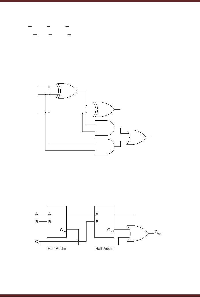
A 1-bit
Full-Adder cane be implemented by
combining together two
Half-Adders. Figure
14.8
∑
∑
∑
∑
∑
Figure14.8
Implementing a
Full-Adder using two
Half-Adders
The
Sum output of the first
Half-Adder is (A ⊕ B)
·
·
The
Carry Out of the first
Half-Adder is AB
The
Sum output of the second
Half-Adder is (A ⊕ B) ⊕ Cin = (A ⊕ B ⊕ Cin )
·
136
CS302 -
Digital Logic & Design
The
Carry Out of the second
Half-Adder is (A ⊕ B)Cin
·
The
output of the OR gate is AB + (A ⊕ B)Cin
·
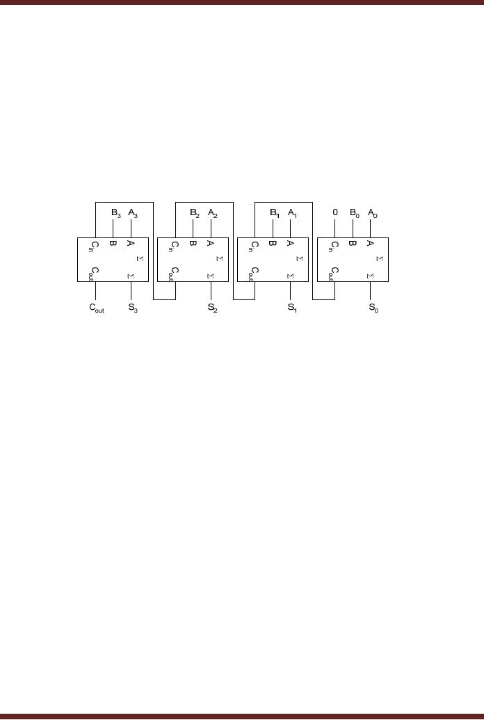
Parallel
Binary Adders
Single
bit Full or Half Adders do
not perform any useful
function. To add two
4-bit
numbers a
4-bit adder is required.
Four single bit Full-Adders
are connected together to
form a
4-bit
Parallel Adder capable of
adding two 4-bit binary
numbers. Figure 14.9.
The
two 4-bit numbers A and B
are applied at the circuit
inputs A0-3 and B0-3
respectively.
The 4-bit Sum output of
the Parallel Adder is
available at outputs S0-3. The
Carry
In to the
circuit is set to 0. (Cin=0). The Carry is
available at Cout.
Figure
14.9
4-bit
Parallel Binary Adder
Carry
Propagation
Parallel
Binary Adders can be
implemented by connecting the
required number of
1-bit
full
adders in a configuration represented in
figure 14.9. However, there
is a practical limitation
to the
number of 1-bit Full-Adders
that can be connected in
parallel. In the 4-bit
Parallel Adder,
the
Most significant bit adder
which adds bits A3, B3 and the
Carry bit C3, can
not proceed until
it receives
the Carry from the
next least significant 1-bit
adder which adds bits
A2, B2. The
A2
B2 bit adder can
not proceed unless it
receives the carry input
C2 from the
A1, B1 adder. The
A1, B1 adder in tern
depends on A0, B0 adder to provide the
carry input. Thus the
carry has to
propagate
through each Full-adder
before it reaches the last
or most significant full
adder.
Assume
that each gate has a
propagation delay of 10 nsec. A
1-bit Full Adder
generates a
Carry out after 30 nsec.
For a 4-bit Parallel Adder
Full-adder the Carry out
from
the
most significant adder would
be after 120 nsec. The
delay can increase to
prohibitive
levels if
8-bit, 16-bit or 64-bit
parallel adders are
implemented. 64-bit parallel
adders are used
by
computers.
Look-Ahead
Carry Circuits
To overcome
the problem of carry
propagation or carry ripple,
Look-Ahead carry
generator
circuits are used. These
circuits look at the bits to
be added and decide if a
higher
order
carry is to be generated. The
Look-Ahead Carry Circuits
although increase the
circuitry
but
they provide a practical
solution to the prohibitive
delays that are caused by
the ripple carry
in parallel
adders.
Consider
the Full-Adder Circuit.
14.10. The output (A ⊕ B) at output P of
the XOR gate
and
the output AB at
output G of the AND gate is
available simultaneously after
one gate
delay. If
the G output of the AND gate
is 1, the Carry Out has to
be a 1 no matter what is
the
137
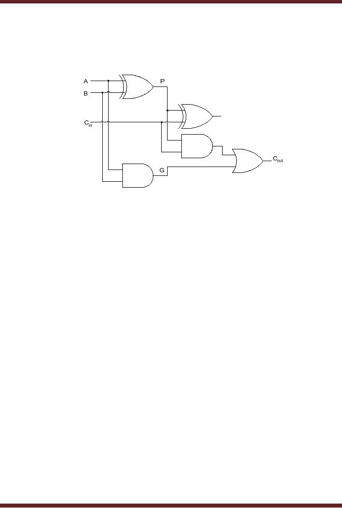
CS302 -
Digital Logic & Design
other
input of the Carry Out OR
gate. The Sum and
Carry Out can be expressed
in terms of P
and G
gate outputs.
· The P
output is called the Carry
Propagate.
· The G
output is called the Carry
Generate
∑
Figure
14.10 Full-Adder with Carry
Generate and Carry
Propagate
Carry
Outputs in terms of Carry
Propagate and Carry
Generate
The
Sum and Carry Out
Boolean expressions can be
rewritten in terms of P,
Carry
Propagate
and G, Carry Generate
terms.
Sum = P ⊕ C
CarryOut
=
CP + G
Writing
the expressions for the
four Carry Out terms
C1, C2, C3 and C4
in terms of
Carry
Propagate P
and Carry Generate G.
C1 = C 0P0 + G0
·
· C 2 = C1P1 + G1 = P1 (C 0P0 + G0 ) + G1 = G1 + P1G0 + P0P1C 0
· C3 = G 2 + P2G1 + P1P2G0 + P0P1P2C0
· C3 = C 2P2 + G 2 = P2 (G1 + P1G0 + P0P1C 0 ) + G 2 = G 2 + P2G1 + P1P2G0 + P0P1P2C 0
· C 4 = G3 + P3G 2 + P2P3G1 + P1P2P3G0 + P0P1P2P3C 0
where
Pn = A n ⊕ Bn and Gn = A nBn
The
Look-Ahead Carry Generator
Circuit is shown. Figure
14.11. The inputs to
the
Look-Ahead
Carry Generator Circuit are
the Carry Propagate terms
P0, P1, P2 and P3
and
Carry
Generate
terms G0, G1, G2 and G3.
The
Carry Propagate P0, P1, P2 and P3 and Carry Generate
terms G1, G2, G3 and G4
are
generated by the XOR and AND
gates after one gate
delay.
The
Outputs of the Look-Ahead
Carry Generator Circuit are
C1, C2, C3 and C4.
The
output
C1 is generated by
the circuit represented by
the expression C1 = C 0P0 + G0 which
138
CS302 -
Digital Logic & Design
requires an AND
gate to generate the product
term C 0P0 and a
second level two input
OR
gate to
sum the terms C 0P0 and G0
. Thus
C1 is available after
two gate delays.
C0
A0
P0
B0
P0
S0
G0
C0
A1
P1
B1
P1
S1
G1
Look-Ahead
C1
Carry
Generator
A2
P2
B2
P2
S2
G2
C2
A3
P3
B3
P3
S3
G3
C3
C4
Figure
14.11 Look-Ahead Carry
Generator
Similarly,
the output C2 is
generated by the circuit
represented by the
expression
C 2 = G1 + P1G0 + P0P1C 0 which
requires a 2-input and
3-input AND gates to generate
the
product
terms P1G0 and P0P1C 0 respectively. A
second level three input OR
gate is required to
sum
the three terms. Thus
C2 is also available
after two gate
delays.
The
output C3 is
generated
by the circuit
represented by
the
expression
C3 = G 2 + P2G1 + P1P2G0 + P0P1P2C0 . The
expression is implemented by a
combination of
three AND gates having 2, 3
and 4 inputs respectively
and a single 4-input
OR
gate.
Again two levels of gates is
used, C3
is available
after a gate delay of
two.
Finally,
the output C4 is generated by
the circuit represented
by the
expression
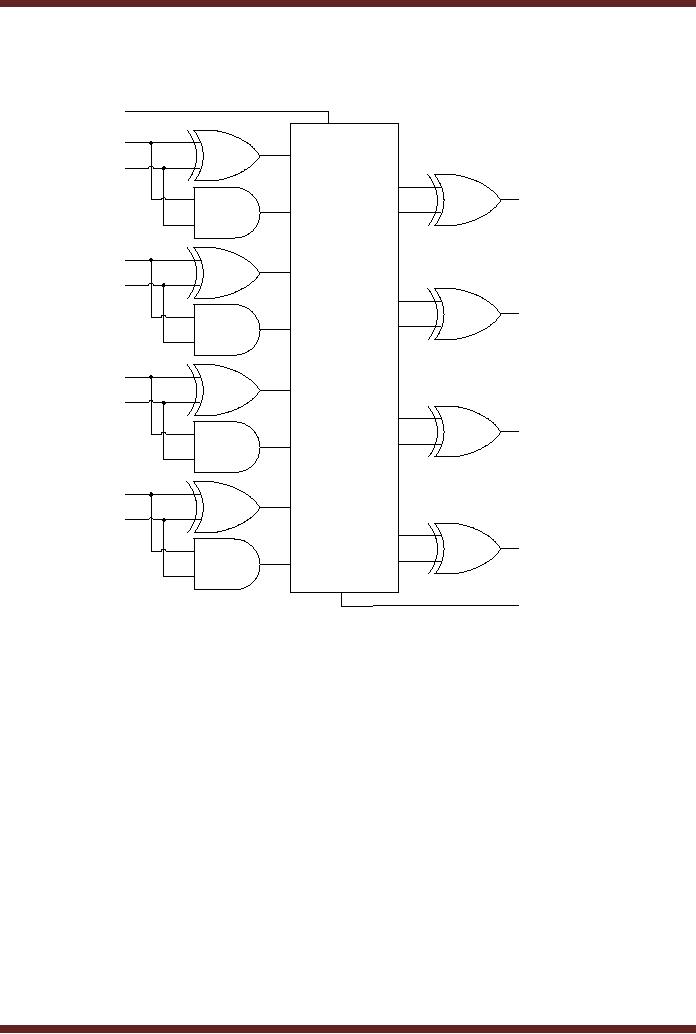
C 4 = G3 + P3G 2 + P2P3G1 + P1P2P3G0 + P0P1P2P3C 0 . To implement
the expression
two
levels of 2, 3, 4 and 5 input AND
gates and a single 5 input
OR gate is used. C4 is
available
after a gate delay of
two.
Thus
for Carry outputs C1, C2, C3 and
C4 the delay is of
the order of two after
the
Propagate
Carry and Generate Carry
terms become
available.
139
CS302 -
Digital Logic & Design
MSI
Adders
4-bit
parallel Adders are
available as Medium Scale
Integrated Circuits. These
circuits
use
the Look-Ahead Carry
Circuitry to remove the
carry ripple. The two
ICS are 74LS83A
and
74LS283.
Both the devices are
functionally identical, however
they are not pin
compatible.
These
devices are packaged as
16-pin devices. The division
of the 16 pins is
· 4 pins
for the 4-bit input
A
· 4 pins
for the 4-bit input
B
· 4 pins
for the 4-bit output
Sum
· 1 pin
for Carry In
· 1 pin
for Carry Out
· 1 pin
for Circuit Power
Supply
· 1 pin
for Circuit GND
The
74LS83A or the 74LS283 can
be cascaded together to form
8-bit, 12-bit or
16-bit
Parallel
Adders. Figure 14.12 The
Carry Out pin of one IC is
connected to the Carry In
pin of
the
other IC.
A
(4-7)
A
(0-3)
A
(8-11)
B
(8-11)
B
(4-7)
B
(0-3)
C12
C8
C4
C0=0
74LS283
74LS283
74LS283
Sum
(8-11)
Sum
(4-7)
Sum
(0-3)
Figure
14.12
12-bit
Parallel Adder using three
74LS283 ICs
140
Table of Contents:
- AN OVERVIEW & NUMBER SYSTEMS
- Binary to Decimal to Binary conversion, Binary Arithmetic, 1s & 2s complement
- Range of Numbers and Overflow, Floating-Point, Hexadecimal Numbers
- Octal Numbers, Octal to Binary Decimal to Octal Conversion
- LOGIC GATES: AND Gate, OR Gate, NOT Gate, NAND Gate
- AND OR NAND XOR XNOR Gate Implementation and Applications
- DC Supply Voltage, TTL Logic Levels, Noise Margin, Power Dissipation
- Boolean Addition, Multiplication, Commutative Law, Associative Law, Distributive Law, Demorgans Theorems
- Simplification of Boolean Expression, Standard POS form, Minterms and Maxterms
- KARNAUGH MAP, Mapping a non-standard SOP Expression
- Converting between POS and SOP using the K-map
- COMPARATOR: Quine-McCluskey Simplification Method
- ODD-PRIME NUMBER DETECTOR, Combinational Circuit Implementation
- IMPLEMENTATION OF AN ODD-PARITY GENERATOR CIRCUIT
- BCD ADDER: 2-digit BCD Adder, A 4-bit Adder Subtracter Unit
- 16-BIT ALU, MSI 4-bit Comparator, Decoders
- BCD to 7-Segment Decoder, Decimal-to-BCD Encoder
- 2-INPUT 4-BIT MULTIPLEXER, 8, 16-Input Multiplexer, Logic Function Generator
- Applications of Demultiplexer, PROM, PLA, PAL, GAL
- OLMC Combinational Mode, Tri-State Buffers, The GAL16V8, Introduction to ABEL
- OLMC for GAL16V8, Tri-state Buffer and OLMC output pin
- Implementation of Quad MUX, Latches and Flip-Flops
- APPLICATION OF S-R LATCH, Edge-Triggered D Flip-Flop, J-K Flip-flop
- Data Storage using D-flip-flop, Synchronizing Asynchronous inputs using D flip-flop
- Dual Positive-Edge triggered D flip-flop, J-K flip-flop, Master-Slave Flip-Flops
- THE 555 TIMER: Race Conditions, Asynchronous, Ripple Counters
- Down Counter with truncated sequence, 4-bit Synchronous Decade Counter
- Mod-n Synchronous Counter, Cascading Counters, Up-Down Counter
- Integrated Circuit Up Down Decade Counter Design and Applications
- DIGITAL CLOCK: Clocked Synchronous State Machines
- NEXT-STATE TABLE: Flip-flop Transition Table, Karnaugh Maps
- D FLIP-FLOP BASED IMPLEMENTATION
- Moore Machine State Diagram, Mealy Machine State Diagram, Karnaugh Maps
- SHIFT REGISTERS: Serial In/Shift Left,Right/Serial Out Operation
- APPLICATIONS OF SHIFT REGISTERS: Serial-to-Parallel Converter
- Elevator Control System: Elevator State Diagram, State Table, Input and Output Signals, Input Latches
- Traffic Signal Control System: Switching of Traffic Lights, Inputs and Outputs, State Machine
- Traffic Signal Control System: EQUATION DEFINITION
- Memory Organization, Capacity, Density, Signals and Basic Operations, Read, Write, Address, data Signals
- Memory Read, Write Cycle, Synchronous Burst SRAM, Dynamic RAM
- Burst, Distributed Refresh, Types of DRAMs, ROM Read-Only Memory, Mask ROM
- First In-First Out (FIFO) Memory
- LAST IN-FIRST OUT (LIFO) MEMORY
- THE LOGIC BLOCK: Analogue to Digital Conversion, Logic Element, Look-Up Table
- SUCCESSIVE APPROXIMATION ANALOGUE TO DIGITAL CONVERTER