 |
Advanced Computer
Architecture-CS501
________________________________________________________
Advanced
Computer Architecture
Lecture
No. 41
Reading
Material
Vincent
P. Heuring & Harry F. Jordan
Computer
Systems Design and Architecture
Summary
Numerical
Examples related to
·
DRAM
·
Pipelining,
Pre-charging and Parallelism
·
Cache
·
Hit Rate
and Miss Rate
·
Access
Time
Example
1
If a DRAM
has 512 rows and its refresh
time is 9ms, what should be
the frequency of
row
refresh operation on the
average?
Solution
Refresh
time= 9ms
Number of
rows=512
Therefore
we have to do 512 row refresh
operations in a 9 ms interval, in other
words
one row
refresh operation every
(9x10⁻³)/512
=1.76x10⁻⁵seconds.
Example
2
Consider
a DRAM with 1024 rows and a refresh
time of 10ms.
a. Find
the frequency of row refresh
operations.
b. What
fraction of the DRAM's time
is spent on refreshing if each refresh
takes 100ns.
Solution
Total
number of rows = 1024
Refresh
period = 10ms
One
row refresh takes place
after every
10ms/1024=9.7micro
seconds
Each row
refresh takes 100ns, so
fraction of the DRAM's time
taken by row refreshes
is,
100ns/9.7
micro sec= 1.03%
Page
358
Last
Modified: 01-Nov-06
Advanced Computer
Architecture-CS501
________________________________________________________
Example
3
Consider
a memory system having the
following specifications. Find
its total cost and
cost per
byte of memory.
Memory
type
Total
bytes
Cost per
byte
SRAM
256
KB
30$ per
MB
DRAM
128
MB
1$ per
MB
Disk
1
GB
10$ per
GB
Solution
Total
cost of system
256 KB( ¼
MB) of SRAM costs = 30 x ¼ =
$7.5
128 MB of DRAM costs=
1 x 128= $128
1 GB of
disk space costs= 10 x
1=$10
Total
cost of the memory
system
=
7.5+128+10=$145.5
Cost per
byte
Total
storage= 256 KB + 128 MB + 1 GB
= 256 KB +
128x1024KB + 1x1024x1024KB
=1,179,904
KB
Total
cost = $145.5
Cost per
byte=145.5/(1,179,904x1024)
=
$1.2x10⁻⁷$/B
Example
4
Find
the average access time of a
level of memory hierarchy if
the hit rate is 80%.
The
memory
access takes 12ns on a hit and 100ns on a
miss.
Solution
Hit rate
=80%
Miss
rate=20%
Thit=12 ns
Tmiss=100ns
Average
Taccess=(hit
rate*Thit)+(miss rate*Tmiss)
=(0.8*12ns)+(0.2*100ns)
=
29.6ns
Page
359
Last
Modified: 01-Nov-06
Advanced Computer
Architecture-CS501
________________________________________________________
Example
5
Consider
a memory system with a cache, a
main memory and a virtual
memory. The
access
times and hit rates are as
shown in table. Find the
average access time for
the
hierarchy.
Main
memory
cache
virtual
memory
Hit
rate
99%
80%
100%
Access
time
100ns
5ns
8ms
Solution
Average
access time for requests
that reach the main
memory
=
(100ns*0.99)+(8ms*0.01)
= 80,099
ns
Average
access time for requests
that reach the cache
=(5ns*0.8)+(80,099ns*0.2)
=16,023.8ns
Example
6
Given
the following memory
hierarchy, find the average
memory access time of
the
complete
system
Memory
type
Average
access time
Hit
rate
SRAM
5ns
80
%
DRAM
60ns
80%
Disk
10ms
100%
Solution
Page
360
Last
Modified: 01-Nov-06
Advanced Computer
Architecture-CS501
________________________________________________________
For
each level, average access
time=( hit rate x access
time for that level) +
((1-hit rate) x
average
access time for next
level)
Average
access time for the
complete system
=
(0.8x5ns) + 0.2 x((0.8x60ns) +
(0.2)(1x10ms))
= 4 +
0.2(48+2000000)
=4 +
400009.6
= 400013.6
ns
Example
7
Find
the bandwidth of a memory
system that has a latency of
25ns, a pre charge time of
5ns and
transfers 2 bytes of data per
access.
Solution
Time
between two memory
references
=latency
+ pre charge time
= 25 ns+
5ns
=
30ns
Throughput
= 1/30ns
=3.33x10⁷ operations/second
Bandwidth
= 2x 3.33x107
=
6.66x10⁷
bytes/s
Example
8
Consider
a cache with 128 byte cache
line or cache block size.
How many cycles does
it
take to
fetch a block from main
memory if it takes 20 cycles to
transfer two bytes of
data?
Solution
The
number of cycles required
for the complete transfer of
the block
=20 x
128/2
= 1280
cycles
Using
large cache lines decreases
the miss rate but it increases
the amount of time a
program
takes to execute as obvious
from the number of clock
cycles required to
transfer
a block
of data into the
cache.
Example
9
Find
the number of cycles
required to transfer the
same 128 byte cache line if
page-mode
DRAM with
a CAS-data delay of 8 cycles is
used for main memory.
Assume that the
cache
lines always lie within a
single row of the DRAM, and
each line lies in a
different
row
than the last line
fetched.
Solution
Page
361
Last
Modified: 01-Nov-06
Advanced Computer
Architecture-CS501
________________________________________________________
Memory
requests to fetch each cache
line=128/2= 64
Only
the first fetch require
the complete 20 cycles, and
the other 63 will take only 8
clock
cycles.
Hence the no. of cycles
required to fetch a cache
line
=20 + 8 x
63
=
524
Example
10
Consider
a 64KB direct-mapped cache
with a line length of 32
bytes.
a.
Determine the number of bits
in the address that refer to
the byte within a
cache
line.
b.
Determine the number of bits
in the address required to select
the cache line.
Solution
Address
breakdown
n=log2 of number of bytes in
line
m=log2 of number of lines in
cache
a. For
the given cache, the
number of bits in the
address to determine the
byte
within
the line= n = log232 = 5
b. There
are 64K/32= 2048 lines in
the given cache. The
number of bits required
to
select
the required line = m
=log22048 = 11
Hence
n=5 and m=11 for this
example.
Example
11
Consider
a 2-way set-associative cache with
64KB capacity and 16 byte
lines.
a.
How many sets are
there in the cache?
b.
How many bits of
address are required to select a
set in the cache?
c.
Repeat the above two
calculations for a 4-way set-associative
cache with
same
size.
Solution
a. A 64KB
cache with 16 byte lines
contains 4096 lines of data. In a
2-way set
associative cache,
each set contains 2 lines,
so there are 2048 sets in
the cache.
b.
Log2(2048)=11. Hence
11 bits of the address are
required to select the
set.
c. The
cache with 64KB capacity and
16 byte line has 4096 lines
of data. For a 4-
way
set associative cache, each
set contains 4 lines, so the
number of sets in the
Page
362
Last
Modified: 01-Nov-06
Advanced Computer
Architecture-CS501
________________________________________________________
cache
would be 1024 and Log 2 (1024) =10. Therefore 10
bits of the address
are
required
to select a set in the
cache.
Example
12
Consider
a processor with clock cycle
per instruction (CPI) = 1.0
when all memory
accesses
hit in the cache. The only
data accesses are loads and stores, and
these constitute
60% of
all the instructions. If the
miss penalty is 30 clock cycles and
the miss rate is
1.5%,
how much faster would
the processor be if all
instructions were cache
hits?
Solution
Without
any misses, the computer
performance is
CPU
execution time = (CPU clock
cycles + Memory stall
cycles) x Clock cycle
=(IC x
CPI+ 0)x Clock cycle = IC x
1.0 x Clock cycle
Now
for the computer with
the real cache, first we
compute the number of memory
stall
cycles:
Memory
accesses
= IC x
Instruction x Miss Rate x Miss
Penalty
Memory
stall cycles
= IC x (l +
0.6) x 0.015 x 30
= IC x
0.72
where
the middle term (1 + 0.6)
represents one instruction access and
0.6 data accesses
per
instruction. The total
performance is thus
CPU
execution time cache = (IC x
1.0 + IC x 0.72) x Clock
cycle
= 1.72 x
IC x Clock cycles
The
performance ratio is the
inverse of the execution
times
CPU
execution time cache = 1.72
x IC x clock cycle
CPU
execution time
1.0 x IC
x clock cycle
The
computer with no cache
misses is 1.72 times
faster
Example
13
Consider
the above example but this
time assume a miss rate of 20 per 1000
instructions.
What is
memory stall time in terms
of instruction count?
Solution
Re
computing the memory stall
cycles:
Memory
stall cycles=Number of misses x
Miss penalty
=IC *
Misses * Miss penalty
Page
363
Last
Modified: 01-Nov-06
Advanced Computer
Architecture-CS501
________________________________________________________
Instruction
=IC /
1000 * Misses * Miss penalty
Instruction
* 1000
=IC /
1000 * 20 * 30
= IC
/1000 * 600= IC * 0.6
Example
14
What
happens on a write
miss?
Solution
The
two options to handle a
write miss are as
follows:
Write
Allocate
The
block is allocated on a write miss,
followed by the write hit
actions. This is just
like
read
miss.
No-Write
Allocate
Here
write misses do not affect
the cache. The block is
modified only in the lower
level
memory.
Example
15
Assume a
fully associative write-back cache with
many cache entries that
starts empty.
Below is
a sequence of five memory
operations (the address is in
square brackets):
Write
Mem[300];
Write
Mem[300];
Read
Mem[400];
Write
Mem[400];
WriteMem[300];
What is
the number of hits and
misses when using no-write
allocate versus write
allocate?
Solution
For
no-write allocate, the
address 300 is not in the cache, and
there is no
allocation
on
write, so
the first two writes will
result in misses. Address 400 is also not
in the cache, so
the
read is also a miss. The subsequent
write to address 400 is a hit.
The last write to 300
is still
a miss. The result for
no-write allocate is four
misses and one hit.
For
write allocate, the first
accesses to 300 and 400 are misses, and
the rest are hits
since
300 and 400
are both found in the
cache. Thus, the result
for write allocate is two
misses
and three
hits.
Example
16
Page
364
Last
Modified: 01-Nov-06
Advanced Computer
Architecture-CS501
________________________________________________________
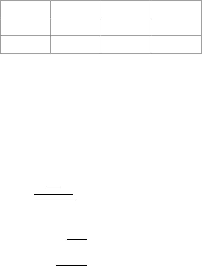
Which
has the lower miss
rate?
a 32 KB
instruction cache with a 32 KB
data cache or a 64 KB unified
cache?
Use the
following Miss per 1000
instructions.
size
Instruction
Data
cache
Unified
cache
cache
32 KB
1.5
40
42.2
64 KB
0.7
38.5
41.2
Assumptions
·
The
percentage of instruction references is
about 75%.
·
Assume
40% of the instructions are
data transfer
instructions.
·
Assume a
hit takes 1 clock
cycle.
·
The miss
penalty is 100 clock
cycles.
·
A load or
store hit takes 1 extra
clock cycle on a unified
cache if there is only
one
cache
port to satisfy two
simultaneous requests.
· Also
the unified cache might lead
to a structural hazard.
· Assume
write-through caches with a
write buffer and ignore
stalls due to the
write
buffer.
What is
the average memory access
time in each case?
Solution
First
let's convert misses per 1000
instructions into
miss
rates.
Misses
Miss rate
=
1000
Instructions
Memory
accesses
Instruction
Since
every instruction access has
exactly one memory access to
fetch the instruction,
the
instruction
miss rate is
Miss
rate32 KB instruction = 1.5/1000 =
0.0015
1.00
Since 40%
of the instructions are data
transfers, the data miss rate
is
Miss Rate
32 kb data = 40 /1000
=
0.1
0.4
Page
365
Last
Modified: 01-Nov-06
Advanced Computer
Architecture-CS501
________________________________________________________
The
unified miss rate needs to account
for instruction and data
accesses:
Miss Rate
64 kb unified = 42.2 /1000 =
0.031
1.00+
0.4
As stated
above, about 75% of the
memory accesses are
instruction references. Thus,
the
overall
miss rate for the split
caches is
(75% x
0.0015) + (25% x 0.1) =
0.026125
Thus, a
64 KB unified cache has a
slightly lower effective miss rate
than two 16 KB
caches.
The average memory access
time formula can be divided
into instruction and
data
accesses:
Average
memory access time
= %
instructions x (Hit time +
Instruction miss rate x Miss Penalty) + %
data x (Hit time
+ Data miss rate x
Miss Penalty)
Therefore,
the time for each
organization is:
Average
memory access time
split
= 75%x(l
+0.0015x 100) + 25%x(l
+0.1x100)
= (75% x
1.15) + (25% x 11)
=
0.8625+2.75= 3.61
Average
memory access time
unified
= 75% x
(1+0.031 x 100) +25% x (1 +
1+0.031 x 100)
= (75% x
4.1) + (25% x 5.1) =
3.075+1.275
=
4.35
Hence
split caches have a better
average memory access time
despite having a
worse
effective
miss rate. Split cache also
avoids the problem of
structural hazard present in a
unified
cache.
Page
366
Last
Modified: 01-Nov-06
Table of Contents:
- Computer Architecture, Organization and Design
- Foundations of Computer Architecture, RISC and CISC
- Measures of Performance SRC Features and Instruction Formats
- ISA, Instruction Formats, Coding and Hand Assembly
- Reverse Assembly, SRC in the form of RTL
- RTL to Describe the SRC, Register Transfer using Digital Logic Circuits
- Thinking Process for ISA Design
- Introduction to the ISA of the FALCON-A and Examples
- Behavioral Register Transfer Language for FALCON-A, The EAGLE
- The FALCON-E, Instruction Set Architecture Comparison
- CISC microprocessor:The Motorola MC68000, RISC Architecture:The SPARC
- Design Process, Uni-Bus implementation for the SRC, Structural RTL for the SRC instructions
- Structural RTL Description of the SRC and FALCON-A
- External FALCON-A CPU Interface
- Logic Design for the Uni-bus SRC, Control Signals Generation in SRC
- Control Unit, 2-Bus Implementation of the SRC Data Path
- 3-bus implementation for the SRC, Machine Exceptions, Reset
- SRC Exception Processing Mechanism, Pipelining, Pipeline Design
- Adapting SRC instructions for Pipelined, Control Signals
- SRC, RTL, Data Dependence Distance, Forwarding, Compiler Solution to Hazards
- Data Forwarding Hardware, Superscalar, VLIW Architecture
- Microprogramming, General Microcoded Controller, Horizontal and Vertical Schemes
- I/O Subsystems, Components, Memory Mapped vs Isolated, Serial and Parallel Transfers
- Designing Parallel Input Output Ports, SAD, NUXI, Address Decoder , Delay Interval
- Designing a Parallel Input Port, Memory Mapped Input Output Ports, wrap around, Data Bus Multiplexing
- Programmed Input Output for FALCON-A and SRC
- Programmed Input Output Driver for SRC, Input Output
- Comparison of Interrupt driven Input Output and Polling
- Preparing source files for FALSIM, FALCON-A assembly language techniques
- Nested Interrupts, Interrupt Mask, DMA
- Direct Memory Access - DMA
- Semiconductor Memory vs Hard Disk, Mechanical Delays and Flash Memory
- Hard Drive Technologies
- Arithmetic Logic Shift Unit - ALSU, Radix Conversion, Fixed Point Numbers
- Overflow, Implementations of the adder, Unsigned and Signed Multiplication
- NxN Crossbar Design for Barrel Rotator, IEEE Floating-Point, Addition, Subtraction, Multiplication, Division
- CPU to Memory Interface, Static RAM, One two Dimensional Memory Cells, Matrix and Tree Decoders
- Memory Modules, Read Only Memory, ROM, Cache
- Cache Organization and Functions, Cache Controller Logic, Cache Strategies
- Virtual Memory Organization
- DRAM, Pipelining, Pre-charging and Parallelism, Hit Rate and Miss Rate, Access Time, Cache
- Performance of I/O Subsystems, Server Utilization, Asynchronous I/O and operating system
- Difference between distributed computing and computer networks
- Physical Media, Shared Medium, Switched Medium, Network Topologies, Seven-layer OSI Model