 |
DIGITAL CLOCK: Clocked Synchronous State Machines |
| << Integrated Circuit Up Down Decade Counter Design and Applications |
| NEXT-STATE TABLE: Flip-flop Transition Table, Karnaugh Maps >> |
CS302 -
Digital Logic & Design
Lesson
No. 30
DIGITAL
CLOCK
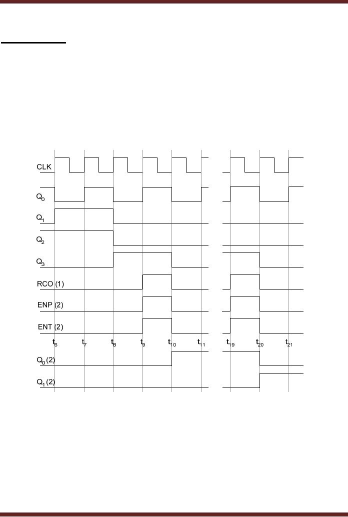
The
timing diagram figure 30.1a
shows the time interval
t6 to t11 and
t19 to t21. At
time
interval
t9 the units
counter counts to 1001 (9)
which is the terminal count
of the 74x160
decade
counter. The RCO signal is
set to logic 1 to indicate
the terminal count. The
RCO
signal is
connected to the ENP and
ENT enable signals of the
tens counter. At interval t10 the
tens
counter is incremented by 1, the
units counter recycles to
0000 (0) and the
RCO signal is
deactivated
inhibiting the tens counter
from incrementing. At interval
t19 the units
counter once
again
reaches its terminal count
activating the RCO signal
and enabling the tens
counter to
increment
its initial count 0001 to
0010. The counting sequence
continues until the
tens
counter
increments to 0101 (5) and
the units counter recycles
to 0000 and continues with
the
counting
sequence on each positive
clock transition.
Figure
30.1a Timing diagram of the
divide by 60 minutes/seconds
counter
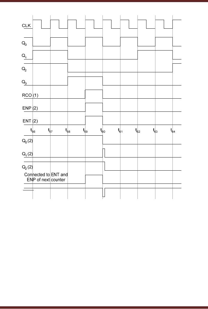
The
timing diagram fig 30.1b
shows the timing sequence
from interval t56 to t64. The unit
counter
reaches its terminal count
at interval t59. The
output of the 3-input AND
gate is set to
logic
high. The output of the AND
gate is connected to the ENP
and ENT enable inputs of
the
next
counter, thus enabling the
next counter. At interval t60, on a positive clock
transition the
units
counter recycles to 0000,
the tens counter increments
to 0110 (6) setting the
output of
the NAND
gate to logic 0 and the
next counter increments its
count. The NAND gate output
is
connected
tot the asynchronous active
low clear input of the
tens counter which is
asynchronously
cleared to 0000.
312
CS302 -
Digital Logic & Design
CLR
Figure
30.1b Timing diagram of the
divide by 60 counter at time
interval t56
to t64
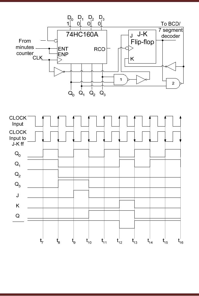
The
hours unit counter circuit
is configured as a decade counter,
counting from 0000 to
1001
when it is enabled by the
Minutes counter circuit. The
NOT gate connected to the
clock
input of
the J-K flip-flop allows
the negative-edge triggered
J-K flip-flop to trigger
when the
units
counter is triggered to count
from 0000 to 1001. The
terminal count 1001 is
detected by
the NAND
gate (1) at interval t9 which sets the J
input of the flip-flop to
logic 1. The K input
of
the
flip-flop is at Logic 0, therefore on a
clock transition at interval
t10 the JK
flip-flop output Q
is set to
logic 1, the units counter
recycles to 0000 resetting J
input to logic 0. The unit
counter
counts to
0001 and 0010 to represent
hours 11 and 12 in interval t11 and t12
respectively.
At
interval
t12 as the unit
counters count changes from
1011 (11) to 1100 (12),
Q1 output is set
to
logic 1,
which sets the output of
the NAND gate to logic 0 as
the other input of the NAND
is
already at
logic 1 (Q). The NAND gate
sets the K input to logic 1
and setting the
active-low
LOAD
signal to logic 0. At interval
t13, at the positive
clock transition the unit
counter is
reloaded
with the count 0001,
the J-K flip-flop output
toggles to logic 0 from
logic 1. As the
units
counter is reloaded with
count 0001, the K input is
set to logic 0. At intervals
t14, t15 and
t16 the hours unit
counter increments the hours
count by 1.
313
CS302 -
Digital Logic & Design
LD
Figure
30.2a Hours Counter
Circuit
LOAD
Figure
30.2b Hours Counter timing
diagram
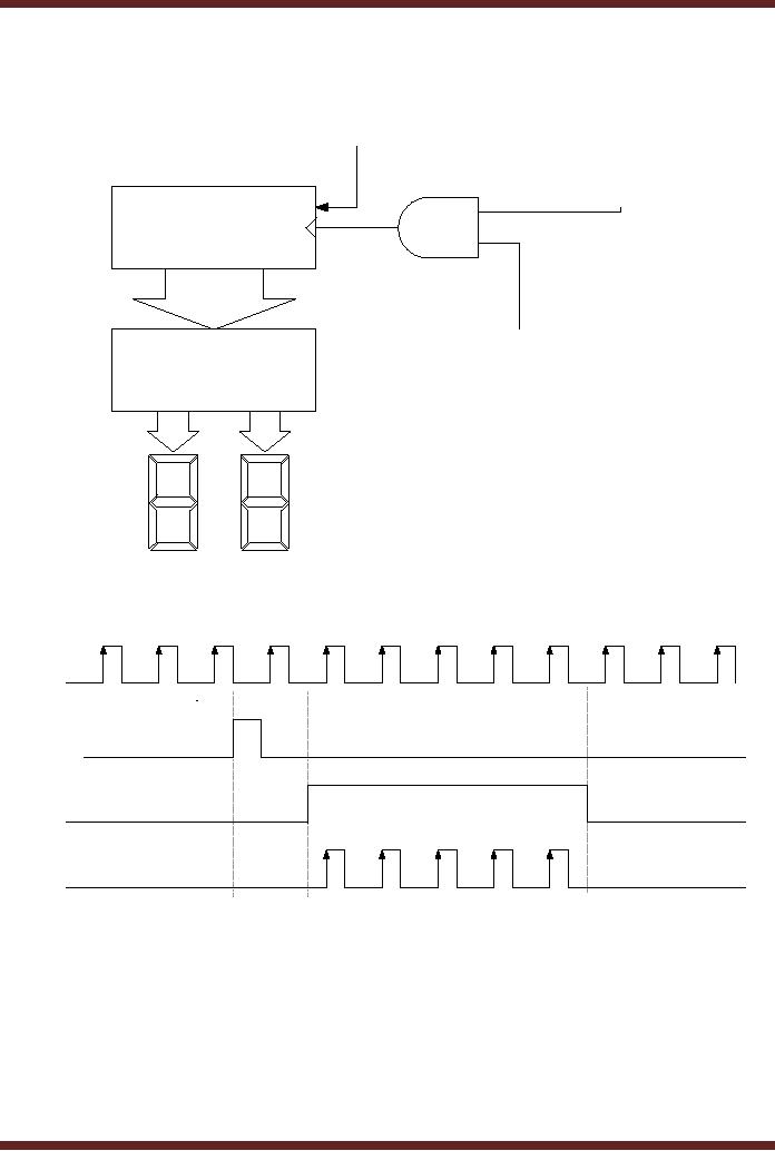
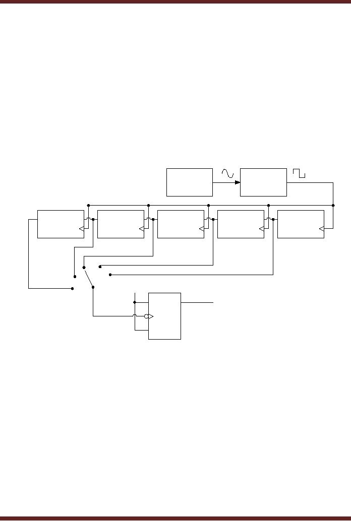
3. Frequency
Counter
A frequency
counter is used to measure
the frequency of an input
signal. The basis
for
the
operation of a frequency counter is
counting of the clock pulses
in a predetermined time
interval.
The frequency of periodic
signal is the number of
cycles in a time period of
one
second.
The frequency of the unknown
signal can be calculated by
counting the number
of
314
CS302 -
Digital Logic & Design
clock
pulses of the unknown signal
and dividing the count
number by the time interval
in which
the
clock pulses are counted,
Figure 30.3
Clear
Input
Signal with
unknown
frequency
Counter
Sampling
BCD &
Segment
Interval
Decoder
a
a
g
g
f
f
b
b
c
c
e
e
d
d
Figure
30.3a Frequency Counter
Circuit
Input
signal
Counter
reset
signal
Sampling
Interval
Counter
Input
t1
t2
t0
Figure
30.3b Timing diagram of the
Frequency Counter
Circuit
In the
circuit shown, the input
signal with unknown
frequency is applied at the
AND
gate
input. The second input of
the AND gate is connected to a
signal which determines
the
sampling
interval. The signal is set
to logic high at interval t1 to enable the AND gate
allowing
the
input signal to be connected to
the clock input of the
counter circuit. The
sampling interval
signal is
set to logic low at the
end of the sampling interval
t2 to disable the AND
gate and
inhibit
the counter from counting.
Before the counter counts
the clock pulses of the
input signal
315
CS302 -
Digital Logic & Design
it is reset by
activating the Asynchronous
input to clear the counter.
At the end of the
sampling
interval
the counter output is
displayed on 7-segment
displays.
The
accuracy of the frequency
counter depends on the
duration of the timing
sampling
interval,
which must be very accurate.
Consider that during a
sampling interval of 1
second
4573
clock pulses of the input
signal are measured. Thus,
the frequency of the unknown
signal
is 4573
Hz. If the same input
signal is sampled using a
0.1 second sampling interval
then
457.3
pulses are counted, which
means that either 457 or
458 will be counted
depending on
the
start of the sampling
interval at t1. Thus
the frequency is determined to be
either 4570 or
4580.
Similarly, if the sampling
interval is reduced to 0.01
seconds, the numbers of
clock
pulses
measured are 45.73, which
means that either 45 or 46
will be read indicating
a
frequency of
4500 or 4600.
100
100
KHz
KHz
Pulse
Crystal
Shaper
Oscillator
Div by
10
Div by
10
Div by
10
Div by
10
Div by
10
100
10
1
10
Hz
Hz
KHz
KHz
1
switch
1
Divide
by
J
Q
Hz
2
output
K
Figure
30.4
Cascaded
Counter circuit for
obtaining accurate sampling
intervals
Very
accurate sampling intervals
are implemented using
cascaded counter which
is
connected to a
very accurate timing signal
generated by a crystal controlled
oscillator (Astable
multi-vibrator).
The output timing signal of
each cascade section is
available at a switch
which
is used to
select the appropriate
timing signal for
controlling the sampling
interval. The output
of the
switch is connected to the
clock input of a negative
triggered J-K flip-flop,
which divides
the
input signal by 2. Thus,
when the 1 Hz sampling
interval is selected, the
signal at the
output of
the J-K flip-flop has a
time period of 2 seconds.
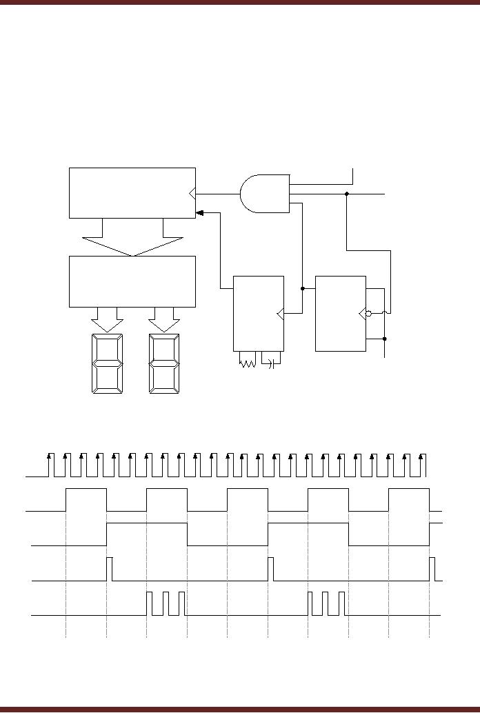
Figure 30.4.
The
detailed circuit diagram and
the timing diagram of the
frequency diagram are
shown in
figure 30.5. In the timing
diagram the Sampling
Interval pulse is obtained
from the
output of
the J-K flip-flop shown in
figure 30.4. The duration of
the Sampling interval pulse
can
be selected
through the switch. The
sampling interval signal is
connected to the input of
the 3-
input AND
gate and the clock
input of the second J-K
flip-flop which toggles its
output at each
negative
transition of the clock.
When the output of the
second flip-flop changes to
logic 1
(interval
t1) it triggers the
One-Shot which generates a
short output pulse which
clears the
316
CS302 -
Digital Logic & Design
Counter
circuit. At interval t2 during the positive
half of the sampling
interval when the output
of
the
second J-K flip-flop is high
the 3-input AND gate is
enabled and the input
signal with
unknown
frequency is applied at the
input of the counter, which
count the input signal
pulses.
At interval
t3 there is negative
transition of the sampling
signal, which triggers the
second flip-
flop
changing its output to logic
0. Logic 0 output of the
flip-flop disables the
3-input AND gate
inhibiting
the counter from counting.
The pulses counted by the
counter during interval t2 to t3
are
directly displayed.
Input
Signal with
unknown
frequency
Counter
Sampling
Clear
Interval
BCD &
Segment
Decoder
Q
Q
J
One
Flip-flop
Shot
2
a
a
K
g
g
f
f
b
b
1
c
c
e
e
d
d
Figure
30.5a Detailed circuit
diagram of a frequency
counter
Input
signal
Sampling
Interval
Output
of
flip-flop
2
Counter
reset
signal
Counter
Input
t0
t1
t2
t3
t4
t5
t6
t7
t8
t9
Figure
30.5b Timing diagram of the
frequency counter
circuit
317

CS302 -
Digital Logic & Design
Design of
Synchronous Counters
The
counters that have been
discussed are binary
counters that count in a
sequence
either
upwards or downwards. The
count start and end
sequence of a counter can
also be set
arbitrarily
and the counter can
then count up or down with
in the terminal count
limits.
Counters
can also be designed that do
not count in a sequence,
instead they sequence
through a
set of predefined arbitrary
values. Counters can also be
implemented using D
flip-
flops
instead of J-K flip-flops. No
formal method of designing
Counters has been
discussed;
however
during the study of
synchronous counters a general
procedure was discussed
which
helps in
the implementation of the
counters. The procedure
requires listing of the
binary
counting
sequence and then
determining the input
condition for each flip-flop
which promotes
a change in
their output state. The
input conditions are
dependent on the previous
start
outputs of
the flip-flops and are
implemented by using logic
gates. The method does
help in
implementing
counters but it is not a
comprehensive method for the
design and
implementation
of different types of
counters.
Clocked
Synchronous State
Machines
The
Synchronous Counters are the
simplest forms of Clocked
Synchronous State
Machines.
State Machine is a generic
name given to Sequential
circuits. The
Sequential
circuits
use a clock signal to change
from one state to the
other and all the
flip-flops are
connected to a
single clock signal,
therefore it is a Clocked Synchronous
State Machine.
A general
Sequential circuit consists of a
combinational circuit and a
memory element. The
memory
element is made of a set of n
flip-flops all connected to a a
common clock. The n
flip-
flops
store 2n
states.
The flip-flops change their
current state to the next
state on each clock
transition.
The next state is determined
by the current state and
the external input. The
output
of the
State Machine is determined by
the current state and
external input. The inputs
to the
memory
which allow the memory to
change its state on a clock
transition are known
as
excitation
inputs or excitation variables.
The present state of the
memory is represented by
state
variables. The state
variables and the inputs to
the sequential circuit
determine the
sequential
circuit output. The
Sequential circuit whose
output depends on the
current state and
the
input is known as Mealy
Machine. Figure
30.6a.
Sequential
circuits whose output
is
determined by
the current state only is
known as Moore Machine.
Figure 30.6b.
318
CS302 -
Digital Logic & Design
Figure
30.6a Clocked Sequential
State Machine (Mealy
Machine)
Figure
30.6b Clocked Sequential
State Machine (Moore
Machine)
Design
Procedure
The
design and implementation of
Synchronous Counters follows
an
established
set of steps and rules
which start from defining
the state diagram and
end at the
implementation
of State machine.
7. State
Diagram
319
CS302 -
Digital Logic & Design
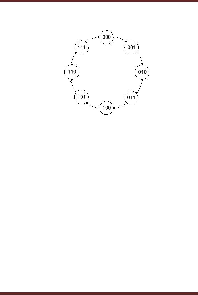
A sequential
circuit (state machine) is
described by a state diagram,
which shows the
sequence of
state through which the
sequential circuit progresses
when it is clocked. The
state
diagram of a
3-bit Synchronous Up-Counter
(sequential circuit) is shown in
the figure. 30.7
Figure
30.7
State
diagram of a 3-bit
Up-Counter
320
Table of Contents:
- AN OVERVIEW & NUMBER SYSTEMS
- Binary to Decimal to Binary conversion, Binary Arithmetic, 1s & 2s complement
- Range of Numbers and Overflow, Floating-Point, Hexadecimal Numbers
- Octal Numbers, Octal to Binary Decimal to Octal Conversion
- LOGIC GATES: AND Gate, OR Gate, NOT Gate, NAND Gate
- AND OR NAND XOR XNOR Gate Implementation and Applications
- DC Supply Voltage, TTL Logic Levels, Noise Margin, Power Dissipation
- Boolean Addition, Multiplication, Commutative Law, Associative Law, Distributive Law, Demorgans Theorems
- Simplification of Boolean Expression, Standard POS form, Minterms and Maxterms
- KARNAUGH MAP, Mapping a non-standard SOP Expression
- Converting between POS and SOP using the K-map
- COMPARATOR: Quine-McCluskey Simplification Method
- ODD-PRIME NUMBER DETECTOR, Combinational Circuit Implementation
- IMPLEMENTATION OF AN ODD-PARITY GENERATOR CIRCUIT
- BCD ADDER: 2-digit BCD Adder, A 4-bit Adder Subtracter Unit
- 16-BIT ALU, MSI 4-bit Comparator, Decoders
- BCD to 7-Segment Decoder, Decimal-to-BCD Encoder
- 2-INPUT 4-BIT MULTIPLEXER, 8, 16-Input Multiplexer, Logic Function Generator
- Applications of Demultiplexer, PROM, PLA, PAL, GAL
- OLMC Combinational Mode, Tri-State Buffers, The GAL16V8, Introduction to ABEL
- OLMC for GAL16V8, Tri-state Buffer and OLMC output pin
- Implementation of Quad MUX, Latches and Flip-Flops
- APPLICATION OF S-R LATCH, Edge-Triggered D Flip-Flop, J-K Flip-flop
- Data Storage using D-flip-flop, Synchronizing Asynchronous inputs using D flip-flop
- Dual Positive-Edge triggered D flip-flop, J-K flip-flop, Master-Slave Flip-Flops
- THE 555 TIMER: Race Conditions, Asynchronous, Ripple Counters
- Down Counter with truncated sequence, 4-bit Synchronous Decade Counter
- Mod-n Synchronous Counter, Cascading Counters, Up-Down Counter
- Integrated Circuit Up Down Decade Counter Design and Applications
- DIGITAL CLOCK: Clocked Synchronous State Machines
- NEXT-STATE TABLE: Flip-flop Transition Table, Karnaugh Maps
- D FLIP-FLOP BASED IMPLEMENTATION
- Moore Machine State Diagram, Mealy Machine State Diagram, Karnaugh Maps
- SHIFT REGISTERS: Serial In/Shift Left,Right/Serial Out Operation
- APPLICATIONS OF SHIFT REGISTERS: Serial-to-Parallel Converter
- Elevator Control System: Elevator State Diagram, State Table, Input and Output Signals, Input Latches
- Traffic Signal Control System: Switching of Traffic Lights, Inputs and Outputs, State Machine
- Traffic Signal Control System: EQUATION DEFINITION
- Memory Organization, Capacity, Density, Signals and Basic Operations, Read, Write, Address, data Signals
- Memory Read, Write Cycle, Synchronous Burst SRAM, Dynamic RAM
- Burst, Distributed Refresh, Types of DRAMs, ROM Read-Only Memory, Mask ROM
- First In-First Out (FIFO) Memory
- LAST IN-FIRST OUT (LIFO) MEMORY
- THE LOGIC BLOCK: Analogue to Digital Conversion, Logic Element, Look-Up Table
- SUCCESSIVE APPROXIMATION ANALOGUE TO DIGITAL CONVERTER