 |
Advanced Computer
Architecture-CS501
Lecture
Handouts
Computer
Architecture
Lecture
No. 12
Reading
Material
Vincent
P. Heuring&Harry F. Jordan
Chapter
4
Computer
Systems Design and Architecture
4.1,
4.2, 4.3
Summary
7) The
design process
8) A
Uni-Bus implementation for
the SRC
9)
Structural RTL for the SRC
instructions
Central
Processing Unit
Design
This
module will explore the
design of the central
processing
unit
from the logic designer's view. A unibus
implementation
of the
SRC is discussed in detail along
with the Data
Path
Design
and
the Control
Unit Design.
The
topics covered in this
module are outlined
below:
1. The
Design Process
2. Unibus
Implementation of the SRC
3.
Structural RTL for the
SRC
4. Logic
Design for one bus SRC
5. The
Control Unit
6. 2-bus
and 3-bus designs
7. The
machine reset
8. The
machine exceptions
As we
progress through this list
of topics, we will learn how to
convert the earlier
specified
behavioral RTL into a concrete
structural RTL. We will also learn
how to
interconnect
various programmer visible registers to
get a complete data path and
how to
incorporate
various control signals into
it. Finally, we will add the
machine reset and
exception
capability to our processor.
The
design process
The
design process of a processor starts with
the specification of the
behavioral RTL for
its
instruction set. This abstract
description is then converted
into structural RTL
which
shows
the actual implementation
details. Since the processor can be
divided into two
main
sub-systems, the data path
and the control unit, we can
split the design
procedure
into
two phases.
Page
150
Last
Modified: 01-Nov-06
Advanced Computer
Architecture-CS501
1. The
data path design
2. The
control unit design
It is
important that the design
activity of these
important
components of the processor be
carried
out
with the pros and cons of adopting
different
approaches
in mind.
As we
know, the execution time is
dependent on
the
following three
factors.
ET = IC x
CPI x T
During
the design procedure we specify
the
implementation
details at an advanced level.
These
details can affect the clock
cycle per
instruction
and the clock cycle time.
Hence
following
things should be kept in
mind during the design
phase.
� Effect
on overall performance
� Amount
of control hardware
� Development
time
Processor
Design
Let us
take a look at the steps
involved in the processor design
procedure.
1.
ISA Design
The
first step in designing a
processor is the specification of
the instruction set
of
the
processor. ISA design includes decisions
involving number and size of
instructions,
formats, addressing modes,
memory organization and
the
programmer's
view of the CPU i.e.
the number and size of general and
special
purpose
registers.
2.
Behavioral RTL Description
In this
step, the behavior of
processor in response to the
specific instructions is
described
in register transfer language.
This abstract description is not
bound to
any
specific implementation of the processor.
It presents only those
static
(registers)
and dynamic aspects (operations) of
the machine that are
necessary to
understand
its functionality. The unit
of activity here is the instruction
execution
unlike
the clock cycle in actual
case. The functionality of
all the instructions
is
described
here in special register transfer
notation.
3.
Implementation of the Data
Path
The
data path design involves decisions
like the placement and
interconnection of
various
registers, the type of flip-flops to be
used and the number and kind
of the
interconnection
buses. All these decisions affect
the number and speed of
register
transfers
during an operation. The
structure of the ALU and the design of
the
memory-to-CPU
interface also need to be decided at
this stage. Then there
are the
control
signals that form the
interface between the data
path and the control
unit.
These
control signals move data
onto buses, enable and disable
flip-flops, specify
the ALU
functions and control the
buses and memory operations.
Hence an
integral
part of the data path design
is the seamless embedding of
the control
signals
into it.
4.
Structural RTL Description
Page
151
Last
Modified: 01-Nov-06
Advanced Computer
Architecture-CS501
In
accordance with the chosen
data path implementation,
the structural RTL for
every
instruction
is described in this step.
The structural RTL is formed
according to the
proposed
micro-architecture which includes
many hidden temporary
registers
necessary
for instruction execution. Since
the structural RTL shows the
actual
implementation
steps, it should satisfy the
time and space requirements of
the CPU as
specified
by the clocking interval and
the number of registers and buses in
the data
path.
5.
Control Unit
Design
The
control unit design is a rather
tricky process as it involves
timing and
synchronization
issues besides the usual
combinational logic used in
the data path
design.
Additionally, there are two
different approaches to the
control unit design;
it
can be
either hard-wired or micro-programmed.
However, the task can be
made
simpler
by dividing the design procedure
into smaller steps as
follows.
a.
Analyze the structural RTL and
prepare a list of control
signals to be
activated
during the execution of each
RTL statement.
b.
Develop logic circuits
necessary to generate the
control signals
c. Tie
everything together to complete
the design of the control
unit.
Processor
Design
A
Uni-bus Data Path
Implementation for the
SRC
In this
section, we will discuss the
uni-bus implementation of the
data path for the
SRC.
But
before we go onto the design
phase, we will discuss what a
data path is. After
the
discussion
of the data path design, we will
discuss the timing step
generation, which
makes
possible the synchronization of the
data path functions.
The
Data Path
The
data path is the arithmetic
portion of the Von Neumann
architecture. It consists of
registers,
internal buses, arithmetic
units and shifters. We have
already discussed the
decisions
involved in designing the
data path. Now we shall
have an overview of the
1-
Bus SRC
data path design. As the name
suggests, this implementation
employs a single
bus for
data flow. After that we
develop each of its blocks
in greater detail and present
the
gate level
implementation.
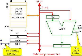
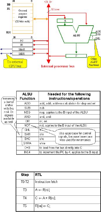
Overview
of the Unibus SRC Data
Path
The
1-bus implementation of the
SRC
data
path is shown in the figure
given.
The
control signals are omitted
here
for
the sake of simplicity.
Following
units
are present in the SRC data
path.
1.
The Register File
The
general-purpose register
file
includes 32 registers R0 to
R31
each 32 bit wide.
These
registers
communicate with
other
components via the internal
processor bus.
2.
MAR
Page
152
Last
Modified: 01-Nov-06
Advanced Computer
Architecture-CS501
The
Memory Address Register takes
input from the ALSU as
the address of the
memory
location to be accessed and transfers
the memory contents on
that
location
onto the memory
sub-system.
3.
MBR
The
Memory Buffer Register has a
bi-directional connection with
both the
memory
sub-system and the registers and ALSU. It
holds the data during
its
transmission
to and from memory.
4.
PC
The
Program Counter holds the
address of the next
instruction to be executed.
Its
value is
incremented after loading of
each instruction. The value
in PC can also be
changed
based on a branch decision in
ALSU. Therefore, it has a
bi-directional
connection
with the internal processor
bus.
5.
IR
The
Instruction Register holds
the instruction that is
being executed. The
instruction
fields are extracted from
the IR and transferred to the
appropriate
registers
according to the external
circuitry (not shown in this
diagram).
6.
Registers A and C
The
registers A and C are required to hold an
operand or result value while
the
bus is
busy transmitting some other
value. Both these registers
are programmer
invisible.
7.
ALSU
There is
a 32-bit Arithmetic Logic
Shift Unit, as shown in the
diagram. It takes
input
from memory or registers via
the bus, computes the
result according to
the
control
signals applied to it, and
places it in the register C,
from where it is
finally
transferred
to its destination.
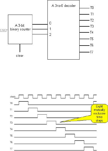
Timing
Step Generator
To ensure
the correct and
controlled
execution of instructions
in a
program, and all the
related
operations,
a timing device is
required.
This is to ensure that
the
operations
of essentially different
instructions
do not mix up in
time.
There
exists a `timing step
generator'
that provides
mutually
exclusive
and sequential timing
intervals.
This is analogous to
the
clock
cycles in the actual processor. A
possible implementation of the timing
step
generator
is shown in the
figure.
Each
mutually exclusive step is
carried out in one timing
interval. The timing
intervals
can be named
T0, T1...T7. The given
figure is helpful in understanding
the `mutual
exclusiveness
in time' of these timing
intervals.
Processor
design
Structural
RTL descriptions of
selected
SRC
instructions
Structural
RTL for the SRC
Page
153
Last
Modified: 01-Nov-06
Advanced Computer
Architecture-CS501
The
structural RTL describes how a
particular operation is performed
using a specific
hardware
implementation. In order to present the
structural RTL we assume that
there
exists a
"timing step generator",
which provides mutually
exclusive and sequential
timing
intervals,
analogous to the clock
cycles in actual processor.
Structural
RTL for Instruction
Fetch
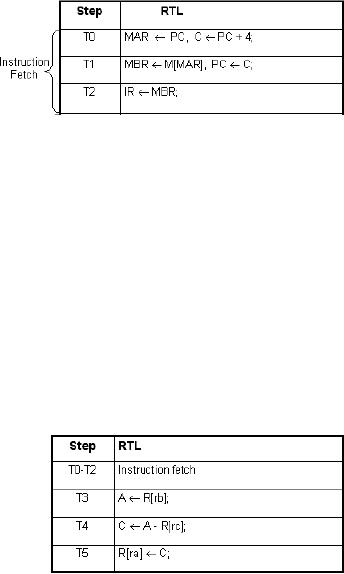
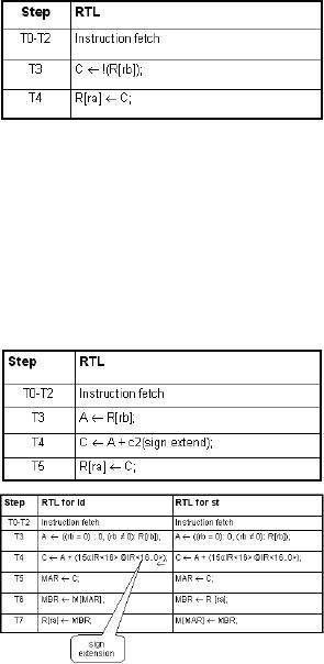
The
instruction fetch procedure
takes three time steps as
shown in the table. During
the
first
time step, T0, address of
the
instruction
is moved to the
Memory
Address
Register (MAR) and value
of
PC is
incremented. In T1 the
instruction
is brought from the
memory
into the Memory
Buffer
Register(MBR),
and the incremented
PC is updated. In
the third and final
time-step of the instruction
fetch phase, the
instruction
from the memory buffer
register is written into the
IR for execution.What
follows
the instruction fetch phase,
is the instruction execution
phase. The number of
timing
steps taken by the execution
phase generally depends on
the type and function
of
instruction.
The more complex the
instruction and its implementation,
the more timing
steps it
will require to complete execution. In
the following discussion, we will take
a
look at
various types of instructions,
related timing steps
requirements and data
path
implementations
of these in terms of the
structural RTL.
Structural
RTL for Arithmetic/Logic
Instructions
The
arithmetic/logic instructions come in two
formats, one with the
immediate operand
and the
other with register operand.
Examples of both are shown
in the following tables.
Register-to-Register
sub
Register-to-register
subtract (or sub) will take
three timing steps to
complete execution,
as shown
in the table. Here we have
assumed
that
the instruction given
is:
sub
ra, rb, rc
Here we
assume that the instruction
fetch
process
has taken up the first
three timing
steps. In
step T3 the internal
register A
receives
the contents of the register
rb. In the next timing
step, the value of register
rc is
subtracted
(since the op-code is sub)
from A. In the final step,
this result is
transferred
into
the destination register ra.
This concludes the
instruction fetch-execute cycle and
at
the end
of it, the timing step
generator is initialized to
T0.
Page
154
Last
Modified: 01-Nov-06
Advanced Computer
Architecture-CS501
The
given figure refreshes
our
knowledge
of the data path. Notice
that
we can
visualize how the steps
that we
have
just outlined can be carried
out, if
appropriate
control signals are
applied
at the
appropriate timing.
As will be
obvious, control signals
need to be applied to the
ALSU, based on the
decoding
of the op-code field of an instruction.
The given table lists
these control
signals:
Note
that we have used
uppercase
alphabets
for naming the
ALSU
functions.
This is to differentiate
these
control
signals from the
actual
operation-code
mnemonics we have
been
using for the
instructions.
The
SHL, SHR, SHC and the
SHRA
functions
are listed assuming that
a
barrel
shifter is available to
the
processor
with signals to
differentiate
between
the various types of shifts
that
are to be
performed.
Structural
RTL for Register-to-Register
add
To enhance
our understanding of the
instruction execution phase
implementation, we will
now take
a look at some more
instructions of
the
SRC. The structural RTL for
a simple add
instruction
add
ra, rb, rc is given
in table.
The
first three instruction
fetch steps are
common to
all instructions. Execution
of
instruction
starts from step T3 where
the first
operand is
moved to register A. The
second
step
involves computation of the
sum and
result is
transferred to the destination in
step T5. Hence the
complete execution of the
add
instruction
takes 6 time steps. Other
arithmetic/logic instructions having
the similar
structural
RTL are "sub",
"and" and "or".
The
only difference is in the T4
step where
the
sign changes to (-), (^), or
(~) according to the
opcode.
Structural
RTL for the not instruction
The
first three steps T0 to T2
are used up in fetching the
instruction as usual. In step
T3,
the
value of the operand specified by
the register is brought into
the ALSU, which will
use
the control function NOT,
negate the value (i.e.
invert it), and the result
moves to the
register
C. In the time step R4,
this result is assigned to
the destination register
through
the
internal bus. Note that we
need control signals to
coordinate all of this; a
control
signal to
allow reading of the
instruction-specified source register in
T3, control signal
for
the selection of appropriate function to
be carried out at the ALSU,
and control signal
Page
155
Last
Modified: 01-Nov-06
Advanced Computer
Architecture-CS501
to allow
only the
instruction-specified
destination
register to read the result
value
from
the data bus.
The
table shown outlines these
steps for the
instruction:
not
ra, rb
Structural
RTL for the addi
instruction
Again,
the first three time
steps are for
the
instruction
fetch. Next, the first
operand is brought into ALSU in
step T3 through
register
A. The
step T4 is of interest here as the
second operand c2 is extracted from
the
instruction
in IR register, sign extended to 32
bits, added to the first
operand and written
into
the result register C. The
execution of instruction completes in
step T5 when the
result is
written into the destination
register. The sign extension
is assumed to be carried
out in
the ALSU as no separate
extension unit is
provided.
Sign
extension for 17-bit c2 is the
same as:(15αIR<16>
�IR<16..0>)
Sign
extension for 22-bit c1 is the
same as:(10αIR<21>
�IR<21..0>)
The
given table outlines the
time steps for the
instruction addi:
Other
instructions that have the
same
structural
RTL are subi, andi
and
ori.
RTL
for the load (ld) and store
(st)
instructions
The
syntax of load instructions
is:
ld
ra, c2(rb)
And
the syntax of store instructions
is:
st
ra, c2(rb)
The
given table outlines the
time steps in
fetching
and executing a load and a store
instruction.
Note that the first 6
time steps (T0
to T5)
for both the instructions
are the same.
The
first three steps are those
of instruction
fetch.
Next, the register A gets
the value of
register
rb, in case it is not zero.
In time step T4, the
constant is sign-extended, and
added
to the
value of register A using
the ALSU. The result is
assigned to register C. Note
that
in the
RTL outlined above, we are sign
extending a field of the
Instruction Register(32-
bit). It
is so because this field is
the constant field in the
instruction, and the
Instruction
Register
holds the instruction in
execution. In step T5, the
value in C is transferred to
the
Memory
Address Register (MAR). This
completes the effective
address calculation of
the
memory
location to be accessed for
the load/ store operation.If it is a
load instruction in
time
step T6, the corresponding
memory location is accessed and
result is stored in
Memory
Buffer Register (MBR). In
step T7, the result is
transferred to the
destination
register
ra using the data bus.If
the instruction is to store the
value of a register, the
time
step T6
is used to store the value of
the register to the MBR. In
the next and final step,
the
value
stored in MBR is stored in the memory
location indexed by the
MAR.We can look
at the
data-path figure and visualize
how all these steps can take
place by applying
appropriate
control signals. Note that,
if more time steps are
required, then a counter
with
more
bits and a larger decoder can be
used, e.g., a 4-bit counter
along with a 4-to-16
decoder
can produce up to 16 time
steps.
Page
156
Last
Modified: 01-Nov-06
Advanced Computer
Architecture-CS501
Page
157
Last
Modified: 01-Nov-06
Table of Contents:
- Computer Architecture, Organization and Design
- Foundations of Computer Architecture, RISC and CISC
- Measures of Performance SRC Features and Instruction Formats
- ISA, Instruction Formats, Coding and Hand Assembly
- Reverse Assembly, SRC in the form of RTL
- RTL to Describe the SRC, Register Transfer using Digital Logic Circuits
- Thinking Process for ISA Design
- Introduction to the ISA of the FALCON-A and Examples
- Behavioral Register Transfer Language for FALCON-A, The EAGLE
- The FALCON-E, Instruction Set Architecture Comparison
- CISC microprocessor:The Motorola MC68000, RISC Architecture:The SPARC
- Design Process, Uni-Bus implementation for the SRC, Structural RTL for the SRC instructions
- Structural RTL Description of the SRC and FALCON-A
- External FALCON-A CPU Interface
- Logic Design for the Uni-bus SRC, Control Signals Generation in SRC
- Control Unit, 2-Bus Implementation of the SRC Data Path
- 3-bus implementation for the SRC, Machine Exceptions, Reset
- SRC Exception Processing Mechanism, Pipelining, Pipeline Design
- Adapting SRC instructions for Pipelined, Control Signals
- SRC, RTL, Data Dependence Distance, Forwarding, Compiler Solution to Hazards
- Data Forwarding Hardware, Superscalar, VLIW Architecture
- Microprogramming, General Microcoded Controller, Horizontal and Vertical Schemes
- I/O Subsystems, Components, Memory Mapped vs Isolated, Serial and Parallel Transfers
- Designing Parallel Input Output Ports, SAD, NUXI, Address Decoder , Delay Interval
- Designing a Parallel Input Port, Memory Mapped Input Output Ports, wrap around, Data Bus Multiplexing
- Programmed Input Output for FALCON-A and SRC
- Programmed Input Output Driver for SRC, Input Output
- Comparison of Interrupt driven Input Output and Polling
- Preparing source files for FALSIM, FALCON-A assembly language techniques
- Nested Interrupts, Interrupt Mask, DMA
- Direct Memory Access - DMA
- Semiconductor Memory vs Hard Disk, Mechanical Delays and Flash Memory
- Hard Drive Technologies
- Arithmetic Logic Shift Unit - ALSU, Radix Conversion, Fixed Point Numbers
- Overflow, Implementations of the adder, Unsigned and Signed Multiplication
- NxN Crossbar Design for Barrel Rotator, IEEE Floating-Point, Addition, Subtraction, Multiplication, Division
- CPU to Memory Interface, Static RAM, One two Dimensional Memory Cells, Matrix and Tree Decoders
- Memory Modules, Read Only Memory, ROM, Cache
- Cache Organization and Functions, Cache Controller Logic, Cache Strategies
- Virtual Memory Organization
- DRAM, Pipelining, Pre-charging and Parallelism, Hit Rate and Miss Rate, Access Time, Cache
- Performance of I/O Subsystems, Server Utilization, Asynchronous I/O and operating system
- Difference between distributed computing and computer networks
- Physical Media, Shared Medium, Switched Medium, Network Topologies, Seven-layer OSI Model