 |
BCD to 7-Segment Decoder, Decimal-to-BCD Encoder |
| << 16-BIT ALU, MSI 4-bit Comparator, Decoders |
| 2-INPUT 4-BIT MULTIPLEXER, 8, 16-Input Multiplexer, Logic Function Generator >> |
CS302 -
Digital Logic & Design
Lesson
No. 17
THE
74XX138 3-TO-8
DECODER
The
3-to-8, 74XX138 Decoder is
also commonly used in
logical circuits. Similar, to
the
2-to-4
Decoder, the 3-to-8 Decoder
has active-low outputs and
three extra NOT
gates
connected at
the three inputs to reduce
the four unit load to a
single unit load. The
3-to-8
Decoder
has three enable inputs,
one of the three enable
inputs is active-high and
the
remaining
two are active-low. All
three enable inputs have to
be activated for the Decoder
to
work.
The function table of the
3-to-8 decoder is presented.
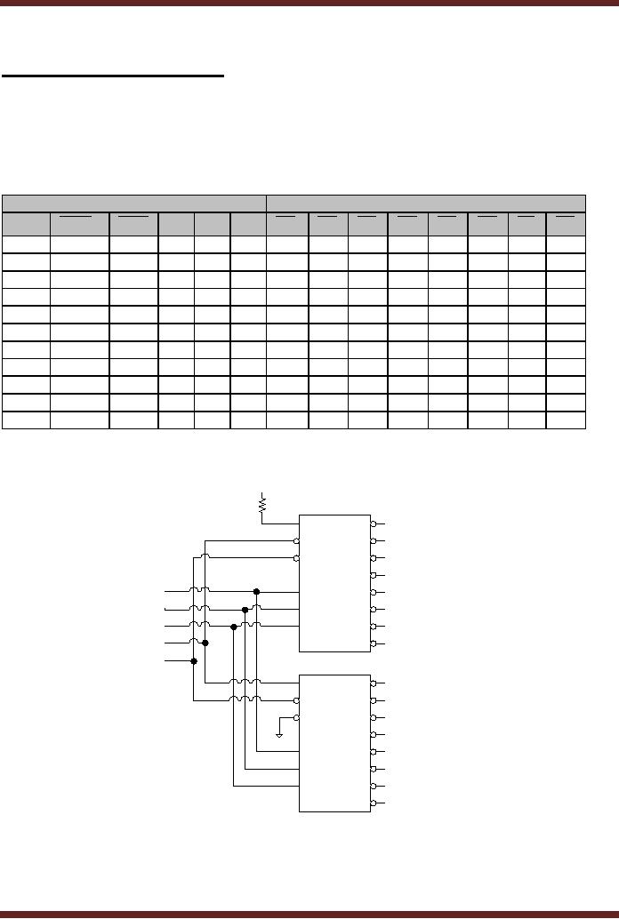
Table 17.1
Inputs
Outputs
G1
C
B
A
G2A
G2B
Y7
Y6
Y5
Y3
Y0
Y4
Y2
Y1
0
X
X
X
X
X
1
1
1
1
1
1
1
1
X
1
X
X
X
X
1
1
1
1
1
1
1
1
X
X
1
X
X
X
1
1
1
1
1
1
1
1
1
0
0
0
0
0
1
1
1
1
1
1
1
0
1
0
0
0
0
1
1
1
1
1
1
1
0
1
1
0
0
0
1
0
1
1
1
1
1
0
1
1
1
0
0
0
1
1
1
1
1
1
0
1
1
1
1
0
0
1
0
0
1
1
1
0
1
1
1
1
1
0
0
1
0
1
1
1
0
1
1
1
1
1
1
0
0
1
1
0
1
0
1
1
1
1
1
1
1
0
0
1
1
1
0
1
1
1
1
1
1
1
Table
17.1
Function
Table of 74LS138, 3-to-8
Decoder
+5V
15
6
Y0
G1
14
4
Y1
G2A
5
13
G2B
Y2
12
Y3
1
11
A
Y4
A
2
10
B
B
Y5
3
9
C
C
Y6
7
D
Y7
enable
6
15
G1
Y0
4
14
G2A
Y1
5
13
G2B
Y2
12
Y3
1
11
A
Y4
2
10
B
Y5
3
9
C
Y6
7
Y7
Figure
17.1
4-to-16
Decoder using two 74LS139,
3-to-8 Decoder
160
CS302 -
Digital Logic & Design
The
three enable inputs serve to
implement to larger Decoders
such as 4-to-16 and 5-to-32
by
cascading
two or four 3-to-8 Decoders
respectively. The connection of
two 3-to-8 Decoders
is
shown.
Figure 17.1
The A, B
and C inputs are connected
directly to the A, B and C
inputs of the two
3-to-8
Decoders.
The D input is connected to
the active-low and
active-high enable inputs G2A
and
G1 of the
two decoders respectively.
The enable input
selects/deselects bothe the
decoders
simultaneously.
G1 and G2B enable inputs of
the two Decoders are
connected to +5v and
Ground
respectively. When the D
input is 0, the upper
decoder is selected and when
D input is
1, the
lower decoder is selected.
The A, B and C inputs serve
to select the appropriate
output
of either
the upper or lower
decoder.
Implementing
Standard SOP and POS
Boolean expressions
The
function table of 3-to-8
Decoder is a table of maxterms.
For example, when
the
input A, B, C is
0, 0 and 0 the Y0 output is
activated indicating the sum
term or maxterm
A + B + C . Similarly, the
A, B and C inputs 1, 0 and 1
activate the Y5 output
indicating the
presence of
A + B + C sum term.
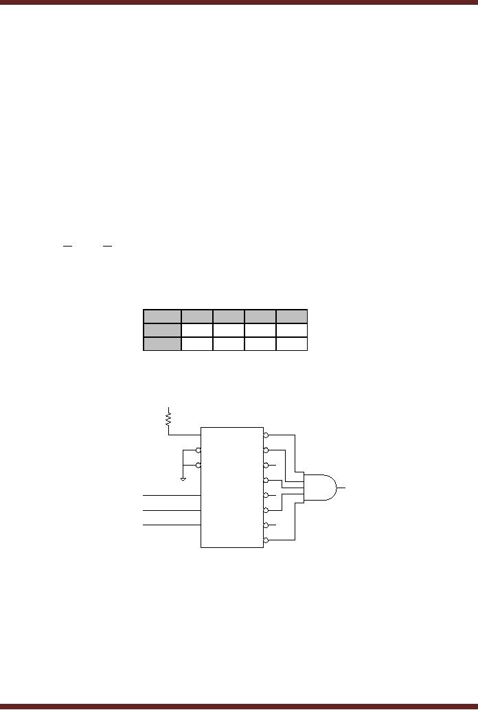
The POS Boolean expression
represented by the
3-variable
Karnaugh
Map, figure 17.2, can be
implemented by the 3-to-8
Decoder which uses an
AND
gate to
implement the product of sum
terms. Figure 17.3
A\BC
00
01
11
10
0
0
0
0
1
1
1
0
0
1
Karnaugh Map of
Boolean expression ∏ ABC
(0,1,3,5,7)
Figure
17.2
+5V
6
15
G1
Y0
4
14
G2A
Y1
5
13
G2B
Y2
12
Y3
1
11
A
A
Y4
2
10
B
B
Y5
3
9
C
C
Y6
7
Y7
Implementation
of Boolean expression ∏ ABC
(0,1,3,5,7)
Figure
17.3
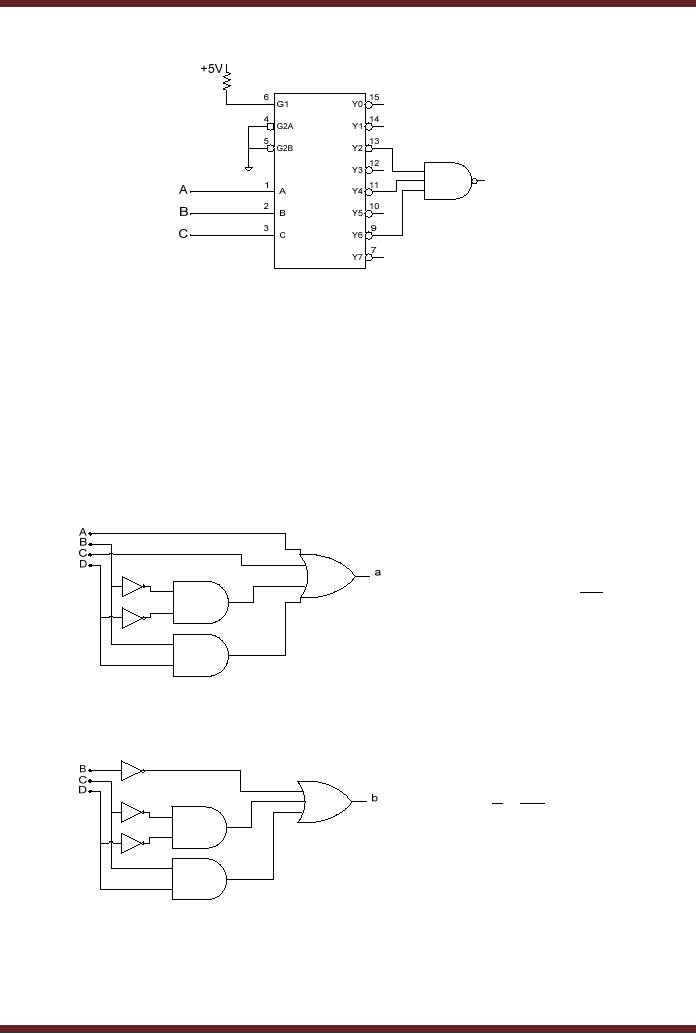
The
3-to-8 Decoder can also be
used to Implement SOP
expression by connecting
the
outputs of
the Decoder to the input of
a NAND gate. Figure 17.4.
The alternate symbol for
the
three
input NAND gate is the three
input OR gate with bubbles
at the inputs. The
three
bubbles
cancel out the three
bubbles connected at the
outputs Y2, Y4 and Y6
representing the
three
minterms or product
terms.
161
CS302 -
Digital Logic & Design
Implementation
of Boolean expression ∑ ABC
(2,4,6)
Figure
17.4
BCD to
7-Segment Decoder
BCD to
7-Segmnet Decoder is a specific
type of decoder that is used
to convert a 4-bit
BCD
Code to a 7-Segment Code.
The BCD to 7-Segment Decoder
unlike the Binary
Decoders
activates
multiple but unique set of
outputs for each 4-bit
BCD input
combination.
Earlier,
the seven expressions for
activating each of the seven
segments were
defined.
Each of
the seven Boolean
expressions can be implemented
using a combination of
NOT-
AND-OR
gates. The implementations
for segments a, b and g are
shown. Figure 17.5a-c
a = A + C + BD + BD
Figure
17.5a Implementation of Segment a
output
b = B + CD + CD
Figure
17.5b Implementation of Segment b
output
162
CS302 -
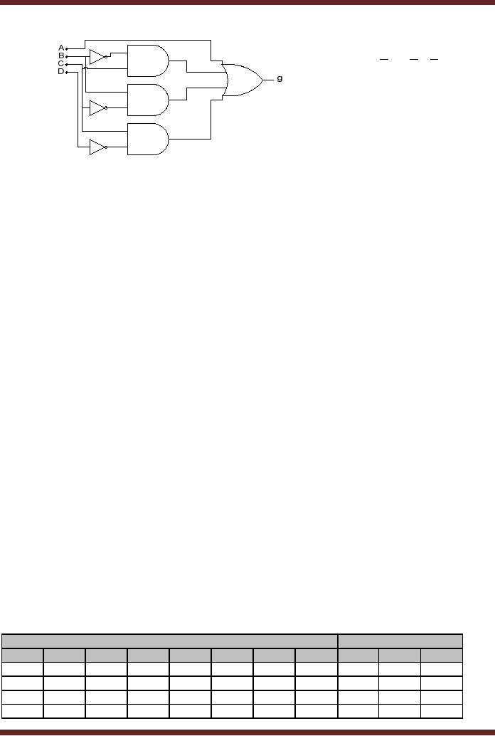
Digital Logic & Design
g = A + BC + CD + BC
Figure
17.5c Implementation of Segment g
output
MSI
Seven-Segment Decoder
The
7-Segment Decoder circuit is
available in MSI form, 74LS47.
The IC has 4-bit
BCD
input
ABCD and 7-bit active-low
outputs for segments a, b, c, d, e, f
and g. The Decoder
also
has
three extra active-low
inputs.
· LT:
Lamp test
· RBI:
Ripple Blanking Input
· BI/RBO:
Blanking Input/Ripple Blanking
Output
When a
low is applied to the LT
input and the BI/RBO is
high, all of the
seven
segments in
the display are turned on to
test that no segments are
burned out. The
Ripple
Blanking
Input and The Blanking
Input/Ripple Blanking Outputs
are used to prevent display
of
leading
and trailing zeros.
BCD-to-Decimal
Decoder
The
operation of the BCD-to-Decimal
Decoder is the same as a
Binary 4-to-16
decoder,
the only difference being
that the BCD-to-Decimal
Decoder has ten output
pins
instead of
sixteen and the input is a
valid BCD number. Thus
invalid BCD codes 1010,
1011,
1100,
1101, 1110 and 1111
applied at the input of the
Decoder do not activate any
of the ten
outputs.
The commercially available
MSI, BCD-to-Decimal Decoder is
the 74LS42, which
has
active-high
inputs and active-low
outputs.
Encoder
An Encoder
functional device performs an
operation which is the
opposite of the
Decoder
function. The Encoder
accepts an active level at
one of its inputs and at
its output
generates a
BCD or Binary output
representing the selected
input. There are various
types of
Encoders
that are used in
Combinational Logic
Circuits.
Binary
Encoder
The
simplest of the Encoders are
the 2n-to-n Encoders.
The functional table and
the
circuit
diagram of an 8-to-3 Binary
Encoder are shown in table
17.2 and figure
17.6
respectively.
Input
Output
I0
I1
I2
I3
I4
I5
I6
I7
O2
O1
O0
X
0
0
0
0
0
0
0
0
0
0
X
1
0
0
0
0
0
0
0
0
1
X
0
1
0
0
0
0
0
0
1
0
X
0
0
1
0
0
0
0
0
1
1
163
CS302 -
Digital Logic & Design
X
0
0
0
1
0
0
0
1
0
0
X
0
0
0
0
1
0
0
1
0
1
X
0
0
0
0
0
1
0
1
1
0
X
0
0
0
0
0
0
1
1
1
1
Table
17.2
Function
Table of an 8-to-3
Encoder
I0
O0
I1
I2
I3
O1
I4
I5
I6
I7
O2
Figure
17.6
8-to-3
Encoder
The
inputs and the outputs of
the 8-to-3 Encoder are
shown to be active-high. The
I0 is
shown to be
unconnected to any gate or
output. Thus, if all inputs
are inactive low, or the
I0
input is
high the output is 000.
The appropriate 3-bit output
combination is activated for
every
input
that is asserted by connecting it to
logic high. The Binary
encoder has a drawback
when
more
than one input is activated.
Consider that the inputs
I3 and I6 are activated
simultaneously
by applying logic 1 at the
two inputs. This results in
the outputs 011 and
110
for
the two inputs respectively.
Thus all three output
pins are at logic 1.
Priority
Encoders
Priority
Encoders remove the problem
highlighted earlier with
simple Binary
Encoders.
Priority
Encoders have necessary
logic to activate the
outputs corresponding to the
highest
Priority
input when multiple inputs
are asserted
simultaneously.
Boolean
expressions for the three
outputs O2, O1 and O0
of an 8-to-3
Priority Encoder
are
can be written in terms of
variables.
O2 = A 7 + A 6 + A 5 + A 4
O1 = A 7 + A 6 + A 3 + A 2
O0 = A 7 + A 5 + A 3 + A1
where
A 7 = I7
164
CS302 -
Digital Logic & Design
A 6 = I7I6
A 5 = I7 I6I5
A 4 = I7 I6 I5I4
A 0 = I7 I6 I5 I4 I3 I2 I1I0
O 2 = I7 + I7I6 + I7 I6I5 + I7 I6 I5I4
= I7 + I7 (I6 + I6I5 + I6 I5I4 ) = I7 + I6 + I6I5 + I6 I5I4 = I7 + I6 + I6 (I5 + I5I4 ) = I7 + I6 + I5 + I5I4
= I7 + I6 + I5 + I4
O1 = I7 + I7I6 + I7 I6 I5 I4I3 + I7 I6 I5 I4 I3I2
= I7 + I7 (I6 + I6 I5 I4I3 + I6 I5 I4 I3I2 ) = I7 + I6 + I6 I5 I4I3 + I6 I5 I4 I3I2 = I7 + I6 + I6 (I5 I4I3 + I5 I4 I3I2 )
= I7 + I6 + I5 I4I3 + I5 I4 I3I2 = I7 + I6 + I5 I4 (I3 + I3I2 ) = I7 + I6 + I5 I4 (I3 + I2 ) = I7 + I6 + I5 I4I3 + I5 I4I2
O 0 = I7 + I7 I6I5 + I7 I6 I5 I4I3 + I7 I6 I5 I4 I3 I2I1
= I7 + I7 (I6I5 + I6 I5 I4I3 + I6 I5 I4 I3 I2I1 ) = I7 + I6I5 + I6 I5 I4I3 + I6 I5 I4 I3 I2I1
= I7 + I6 (I5 + I5 I4I3 + I5 I4 I3 I2I1 ) = I7 + I6 (I5 + I5 (I4I3 + I4 I3 I2I1 )) = I7 + I6 (I5 + I4I3 + I4 I3 I2I1 )
= I7 + I6 (I5 + I4 (I3 + I3 I2I1 )) = I7 + I6 (I5 + I4 (I3 + I2I1 )) = I7 + I6I5 + I6 I4I3 + I6 I4 I2I1
The
MSI, 74XX148 8-input
Priority has a circuit
implemented based on the
Boolean
expression
for outputs O0, O1 and O2.
The function table of the
8-inpuy Priority Encoder
is
presented.
Table 17.3
Inputs
Outputs
E1
I1
I2
I4
A2
A1
I0
I3
I5
I6
I7
A0
GS
EO
1
X
X
X
X
X
X
X
X
1
1
1
1
1
0
X
X
X
X
X
X
X
0
0
0
0
0
1
0
X
X
X
X
X
X
0
1
0
0
1
0
1
0
X
X
X
X
X
0
1
1
0
1
0
0
1
0
X
X
X
X
0
1
1
1
0
1
1
0
1
0
X
X
X
0
1
1
1
1
1
0
0
0
1
0
X
X
0
1
1
1
1
1
1
0
1
0
1
0
X
0
1
1
1
1
1
1
1
1
0
0
1
0
0
1
1
1
1
1
1
1
1
1
1
0
1
0
1
1
1
1
1
1
1
1
1
1
1
1
0
Table
17.3
Function
Table of an 8-Input Priority
Encoder
Cascading
Priority Encoders
The
74XX148 Priority Encoder has
active-low inputs and
active-low outputs.
The
Encoder
also has an active-low
enable input E1 which
enables or disables the
outputs. The
Group
Select GS active-low output is
asserted when any one of
the inputs is asserted.
The
165
CS302 -
Digital Logic & Design
Enable
output EO signal is used to
cascade multiple Encoders to
form larger Encoders.
The
EO output is
connected to the EI input of
the Encoder which handles
lower priority inputs.
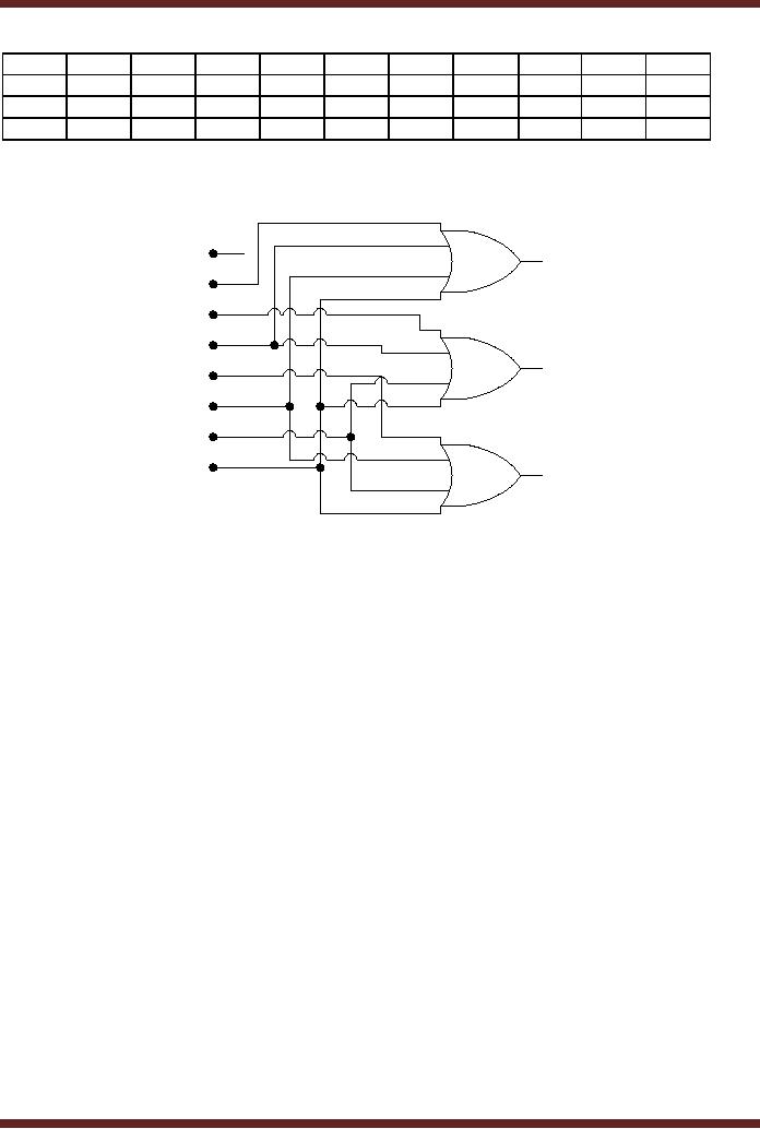
Two
8-input
are shown connected together
to form a 16-input Priority
Encoder. Figure 17.7
Figure
17.7
8-input
Priority Encoders connected to
form a 16-input Priority
Encoder
Decimal-to-BCD
Encoder
The
Decimal-to-BCD Encoder has
ten inputs, for the
decimal digits 0 to 9 and
four
outputs
corresponding to the 4-bit
BCD output. The 74LS147 is a
Decimal-to-BCD Priority
Encoder
which has active-low input
and outputs. The
Decimal-to-BCD Priority Encoder is
used
as a keypad
encoder. A telephone keypad
has digits 0 to 9. The
keypad is connected to
the
encoder
through pull-up resistors
that ensure that the
inputs to the encoder are
logic high
when
none of the keypad keys is
pressed. When ever a key is
pressed the appropriate
input of
the
encoder is connected to logic
low and at the output
the corresponding BCD code
is
generated.
Figure 17.8
166
CS302 -
Digital Logic & Design
Figure
17.8
Keypad
Encoder
Multiplexer
Multiplexer is a
digital switch that has
several inputs and a single
output. The
Multiplexer
also has select inputs
that allow any one of
the multiple inputs can be
selected to
be connected to
the output. Multiplexers are
also known as Data
Selectors. The main use
of
the
Multiplexer is to select data
from multiple sources and to
route it to a single Destination.
In
a computer,
the ALU combinational circuit
has two inputs to allow
arithmetic operations to be
performed on
two quantities. The two
quantities are usually
stored in different set of
registers.
The
inputs of the two
multiplexers are connected to
the output of each of the
multiple registers.
The
outputs of the two
multiplexers are connected to
the two inputs of the
ALUs. The
Multiplexers
are used to route the
contents of any two
registers to the ALU
inputs.
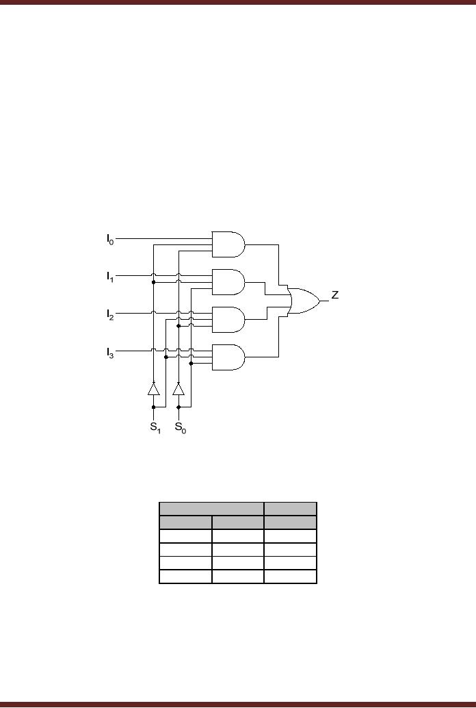
Multiplexers
are available in different
configurations. The 4-to-1
Multiplexer circuit is
shown.
Figure 17.9, the function
table of the Multiplexer is
presented. Table 17.4
Figure
17.9
4-to-1
Multiplexer
Select
Inputs
Output
S1
S0
Z
0
0
I0
0
1
I1
1
0
I2
1
1
I3
Table
17.4
Function
table of 1-to-4
Multiplexer
When
the Select input are
set to 00, the first AND
gate at the top is enabled
allowing
the
logic high or low applied at
input I0
to be routed
through the OR gate to the
output Z.
Similarly,
when the Select input is
set to 10 the third gate is
enabled allowing the logic
value
applied at
the input I2 to be
routed through the OR gate
to the output Z.
167
CS302 -
Digital Logic & Design
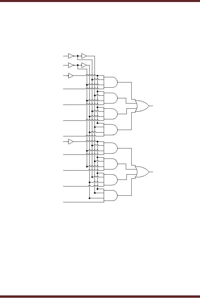
1. Dual
4-Input Multiplexer
Commercial
available 4-input Multiplexer is
the 74XX153 IC which has
two 4-input
multiplexers.
The two select inputs of
the two 4-input multiplexers
are common, however
each
multiplexer
has a separate enable input
which allows the two
multiplexers to be separately
controlled.
The circuit diagram of the
dual 4-input multiplexers is
shown. Figure 17.10
A
B
1G
1C0
1C1
1Y
1C2
1C3
2G
2C0
2C1
2Y
2C2
2C3
Figure
17.10 Dual, 4-input
Multiplexer
Both
the 4-input Multiplexers
have active-high inputs and
outputs. The first
Multiplexer
has
the inputs 1C0, 1C1,
1C2 and 1C3 and
the output 1Y. The
multiplexer has an
active-low
enable
signal defined by 1G. The
select inputs are defined by
A and B which are both
active-
high.
Two extra NOT gates
are connected at the select
inputs to reduce the unit
load from 5
each to
one. Similar to the 4-input
Multiplexer discussed earlier,
the select input lines
enable
one of
the four AND gates and
allow the corresponding
input logic value to be
routed to the
output
through the OR gate. The
second 4-input Multiplexer is
identical it has
active-high
inputs
defined by 2C0, 2C1, 2C2
and 2C3 and an active-high
output defined by 2Y.
The
multiplexer
has an independent active-low
enable signal that
enables/disables the four
AND
gates.
The select inputs A and B
controlling the first
multiplexer also control the
second
multiplexer.
168
Table of Contents:
- AN OVERVIEW & NUMBER SYSTEMS
- Binary to Decimal to Binary conversion, Binary Arithmetic, 1s & 2s complement
- Range of Numbers and Overflow, Floating-Point, Hexadecimal Numbers
- Octal Numbers, Octal to Binary Decimal to Octal Conversion
- LOGIC GATES: AND Gate, OR Gate, NOT Gate, NAND Gate
- AND OR NAND XOR XNOR Gate Implementation and Applications
- DC Supply Voltage, TTL Logic Levels, Noise Margin, Power Dissipation
- Boolean Addition, Multiplication, Commutative Law, Associative Law, Distributive Law, Demorgans Theorems
- Simplification of Boolean Expression, Standard POS form, Minterms and Maxterms
- KARNAUGH MAP, Mapping a non-standard SOP Expression
- Converting between POS and SOP using the K-map
- COMPARATOR: Quine-McCluskey Simplification Method
- ODD-PRIME NUMBER DETECTOR, Combinational Circuit Implementation
- IMPLEMENTATION OF AN ODD-PARITY GENERATOR CIRCUIT
- BCD ADDER: 2-digit BCD Adder, A 4-bit Adder Subtracter Unit
- 16-BIT ALU, MSI 4-bit Comparator, Decoders
- BCD to 7-Segment Decoder, Decimal-to-BCD Encoder
- 2-INPUT 4-BIT MULTIPLEXER, 8, 16-Input Multiplexer, Logic Function Generator
- Applications of Demultiplexer, PROM, PLA, PAL, GAL
- OLMC Combinational Mode, Tri-State Buffers, The GAL16V8, Introduction to ABEL
- OLMC for GAL16V8, Tri-state Buffer and OLMC output pin
- Implementation of Quad MUX, Latches and Flip-Flops
- APPLICATION OF S-R LATCH, Edge-Triggered D Flip-Flop, J-K Flip-flop
- Data Storage using D-flip-flop, Synchronizing Asynchronous inputs using D flip-flop
- Dual Positive-Edge triggered D flip-flop, J-K flip-flop, Master-Slave Flip-Flops
- THE 555 TIMER: Race Conditions, Asynchronous, Ripple Counters
- Down Counter with truncated sequence, 4-bit Synchronous Decade Counter
- Mod-n Synchronous Counter, Cascading Counters, Up-Down Counter
- Integrated Circuit Up Down Decade Counter Design and Applications
- DIGITAL CLOCK: Clocked Synchronous State Machines
- NEXT-STATE TABLE: Flip-flop Transition Table, Karnaugh Maps
- D FLIP-FLOP BASED IMPLEMENTATION
- Moore Machine State Diagram, Mealy Machine State Diagram, Karnaugh Maps
- SHIFT REGISTERS: Serial In/Shift Left,Right/Serial Out Operation
- APPLICATIONS OF SHIFT REGISTERS: Serial-to-Parallel Converter
- Elevator Control System: Elevator State Diagram, State Table, Input and Output Signals, Input Latches
- Traffic Signal Control System: Switching of Traffic Lights, Inputs and Outputs, State Machine
- Traffic Signal Control System: EQUATION DEFINITION
- Memory Organization, Capacity, Density, Signals and Basic Operations, Read, Write, Address, data Signals
- Memory Read, Write Cycle, Synchronous Burst SRAM, Dynamic RAM
- Burst, Distributed Refresh, Types of DRAMs, ROM Read-Only Memory, Mask ROM
- First In-First Out (FIFO) Memory
- LAST IN-FIRST OUT (LIFO) MEMORY
- THE LOGIC BLOCK: Analogue to Digital Conversion, Logic Element, Look-Up Table
- SUCCESSIVE APPROXIMATION ANALOGUE TO DIGITAL CONVERTER