 |

Chapter
Six
OPTICAL
RECEIVER CIRCUITS
The
overall task of the optical
receiver is to extract the
information that has been
placed on the
modulated
light carrier by the distant
transmitter and restores the
information to its original
form.
The
typical through-the-air communications
receiver can be broken down
into five separate
sections.
These are: light collector (lens),
light detector (PIN),
current to voltage converter,
signal
amplifier
and pulse discriminator. There
may also be additional circuits
depending on the kind
of
the
signal being received. As an
example, a receiver that is
extracting voice information will
need a
frequency
to voltage converter and an audio
amplifier to reproduce the
original voice
signal.
Computer
data receivers will also need
some decoding circuits that
would configure the
transmitted
serial
data bits into 8 bit
words. However, this section
will concentrate on the circuits
needed for
processing
voice information. Volume II of
this book will contain
additional circuits for
digital data
receivers.
Light
Collector
For
long-range applications it is essential to
collect the weak modulated
light from the
distant
transmitter
with a glass or plastic lens
and focus it onto a silicon
PIN photodiode. Although
mirrors
could
also be used to collect the
light, glass or plastic
lenses are easier to use and
cost less. Plastic
lenses
measuring from a fraction of an
inch to six inches are
available. For a system that
demands a
large
lens, the flat "Fresnel"
lens is much less expensive
than a solid lens. Forming
special
concentric
bumps in a clear plastic
sheet makes Fresnel lenses.
The bumps bend the light
just as a
conventional
thick lens would. Fresnel
lenses are available with
diameters of several feet.
For
certain short-range applications it
may also be possible to use a naked light
detector without any
lens.
Distances up to several hundred feet
are possible with systems that
don't rely on lenses
at
either
the transmitter or the
receiver. Lens-less systems are
especially useful when very
wide
acceptance
angles are required. Many cordless IR
stereo headsets use two or
more naked detectors
to
provide acceptance angles approaching 360
degrees.
The
lens chosen should be as large as
possible but not too large.
A lens that is too large can
produce
a
half angle acceptance angle
that is too small.
Acceptance angles less than
about 0.3 degrees
will
result
in alignment difficulties. Building
sway and atmospheric disturbances can
cause signal
disruption
with narrow acceptance angles. A
rough rule-of-thumb might be
that the lens
diameter
should
not be more than 100 times
larger than diameter of the
active area of the PIN
detector. Also,
the
receiver should never be
positioned so sunlight could be
focused onto the light
detector. Even a
brief
instant of focused sunlight will
destroy the sensor. A north/south
alignment for the
transmitter
and
the receiver will usually
prevent an optical system
from going blind from
focused sunlight.
Light
Detector
As
discussed in the section on
light detectors, the silicon
PIN photodiode is the
recommended
detector
for most all through-the-air
communications. Such a detector
works best when
reversed
Page
43
of 68
Optical
Through-the-Air Communications Handbook
-David A. Johnson, PE
biased.
In the reversed biased mode it becomes a
diode that leaks current in response to
the light
striking
it. The current is directly
proportional to the incident
light power level (light
intensity).
When
detecting light at its peak
spectrum response wavelength of 900
nanometers, the silicon
PIN
photodiode
will leak about 0.5 micro
amps of current for each
microwatt of light striking
it. This
relationship
is independent to the size of the
detector. The PIN photodiode
size should be chosen
based
on the required frequency
response and the desired
acceptance angle with the
lens being used.
Large
PIN photodiodes will have
slower response times than
smaller devices. For example, 1 cm
X
1
cm diodes should not be used
for modulation frequencies
beyond 200KHz, while 2.5 mm
X 2.5
mm
diodes will work beyond
50MHz. If a long range is desired, the
largest photodiode possible
that
will
handle the modulation
frequency should be
used.
Stray
Light Filters
Some
systems can benefit from the
placement of an optical filter
between the lens and
the
photodiode.
The filter can reduce the
effects of sunlight and some
stray light from distant
street
lamps.
Filters can be especially effective if
the light detector is going
to be processing light from a
diode
laser. Since laser light has a
very narrow bandwidth, an
optical band pass filter
that perfectly
matches
the laser light can make a light
receiver nearly blind to
stray sunlight.
If
light emitting diode light
sources are used, optical
filters with a much broader
bandwidth are
needed.
Such a filter may be needed
for some situations where
man-made light is severe.
Many
electronically
controlled fluorescent and metal
vapor lamps can produce
unwanted modulated
light
that
could interfere with the
light from the distant
transmitter.
But,
in all but a few rare
exceptions, band pass filters
produce few overall
improvements if the
correct
detector circuit is used. Since no
optical filter is perfectly
transparent, the noise
reduction
benefits
of the filter usually do not
out weigh the loss of light
through the filter. Also, if
the detector
is
going to process mostly
visible light, no optical
filter should be
used.
Current
to Voltage Converter Circuits
The
current from the PIN
detector is usually converted to a
voltage before the signal is
amplified.
The
current to voltage converter is
perhaps the most important
section of any optical
receiver
circuit.
An improperly designed circuit will
often suffer from excessive noise
associated with
ambient
light focused onto the
detector. Many published
magazine circuits and even
many
commercially
made optical communications systems
fall short of achievable goals
from poorly
designed
front-end circuits. Many of
these circuits are greatly
influenced by ambient light
and
therefore
suffer from poor sensitivity
and shorter operating ranges
when used in bright
light
conditions.
To get the most from your
optical through-the-air system
you need to use the
right front-
end
circuit.
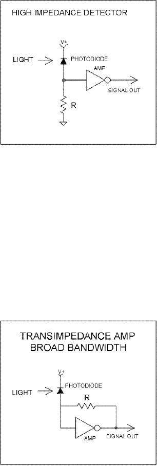
High
Impedance Detector
Circuit
One
method that is often shown
in many published circuits, to
convert the leakage current
into a
voltage,
is illustrated in figure
6a.
This simple "high impedance"
technique uses a resistor
to
develop
a voltage proportional to the
light detector current.
However, the circuit suffers
from
several
weaknesses. If the resistance of
the high impedance circuit is
too high, the leakage
current,
caused
by ambient light, could saturate
the PIN diode, preventing
the modulated signal from
ever
being
detected. Saturation occurs when
the voltage drop across
the resistor, from the
photodiode
Page
44
of 68
Optical
Through-the-Air Communications Handbook
-David A. Johnson, PE
leakage
current, approaches the
voltage used to
bias
the PIN device. To prevent
saturation, the PIN
must
maintain a bias voltage of at least a
few volts.
Consider
the following example. Under
certain
bright
background conditions a PIN
photodiode
leakage
current of a few milliamps
may be
possible.
If a 12v bias voltage were
used, the
detector
resistance would have to be
less than
10,000
ohms to avoid saturation.
With a 10K
resistor,
the conversion would then be
about 10
millivolts
for each microamp of PIN
leakage
current.
But, to extract the weak
signal of interest
that
may be a million times
weaker than the
ambient
light level, the resistance
should to be as
Figure
6a
high
as possible to get the best current to
voltage
conversion.
These two needs conflict
with each other in the
high impedance technique and will
always
yield a less than desirable
compromise.
In
addition to a low current to
voltage conversion, there is also a
frequency response penalty
paid
when
using a simple high impedance
detector circuit. The
capacitance of the PIN diode and
the
circuit
wiring capacitance all tend
to act as frequency filters and will
cause the circuit to have
a
lower
impedance when used with the
high frequencies associated
with light pulses. Furthermore,
the
high
impedance technique also does not
discriminate between low or
high frequency light
signals.
Flickering
streetlights, lightning flashes or
even reflections off distant
car windshields could be
picked
up along with the weak
signal of interest. The high
impedance circuit is therefore
not
recommended
for long-range optical
communications.
Transimpedance
Amplifier Detector Circuit
With Resistor
Feedback
An
improvement over the high
impedance method
is
the "transimpedance amplifier" as
shown in
figure
6b. The
resistor that converts the
current to a
voltage
is connected from the output
to the input of
an
inverting amplifier. The
amplifier acts as a
buffer
and produces an output voltage
proportional
to
the photodiode current. The
most important
improvement
the transimpedance amplifier
has
over
the simple high impedance
circuit is its
canceling
effect of the circuit wiring
and diode
capacitance.
The effective lower capacitance
allows
the
circuit to work at much
higher frequencies.
However,
as in the high impedance method,
the
circuit
still uses a fixed resistor
to convert the
current
to a voltage and is thus prone to
saturation
Figure
6b
and
interference from ambient
light.
Page
45
of 68
Optical
Through-the-Air Communications Handbook
-David A. Johnson, PE
Transimpedance
Amplifier Detector Circuit
With Inductor
Feedback
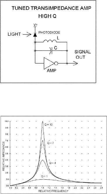
A
dramatic improvement of the
transimpedance
amplifier
with a resistor feedback load is
shown
in
figure
6c. This
technique is borrowed
from
similar
circuits used in radio
receivers. The
circuit
replaces the resistor with
an inductor. A
student
in electronics may remember
that an
inductor
will pass DC unaffected but
will
exhibit
a resistance effect or reactance to
AC
signals.
The higher the frequency of
the AC
signals
the higher the reactance.
This reactance
circuit
is exactly what is needed to
help extract
the
sometimes small modulated AC light
signal
from
the large DC component
caused by
unmodulated
ambient light. DC signals
from
ambient
light will yield a low
current to voltage
conversion
while high frequency AC
signals
Figure
6c
will
experience a high current to
voltage
conversion.
With the right circuit, an
AC vs. DC conversion ratio of
several million is possible.
Such
techniques are used
throughout radio receiver
circuits to process weak
signals.
In
addition, as the Q increases so
does the
impedance
of the LC circuit. Such high
Q
circuits
can also be used in
a
transimpedance
amplifier designed
for
optical
communications. To obtain
the
highest
possible overall impedance, the
inductance
value should be as large
as
possible
and the capacitance should be
as
small
as possible. Since every inductor
contains
some finite parallel
capacitance
within
its assembly, the highest
practical
impedance
occurs when only
the
capacitance
associated with the
inductor
assembly
is used to form the LC
network.
In
radio, connecting a capacitor in
parallel
Figure
6d
with
the inductor often produces
high impedances and allowing
the LC tuned circuit to
resonant at a
specific
frequency. Such a circuit can be
very frequency selective and can
yield impedances of
several
mega ohms. The degree of
rejection to frequencies outside
the center resonant
frequency is
defined
as the "Q" of the circuit.
As figure
6d
depicts, a
high Q will produce a narrower
acceptance
band
of frequencies than lower Q
circuits.
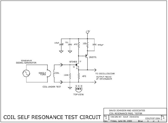
You
can calculate the equivalent
parallel capacitance of an inductor based
on the published
"self-
resonance"
frequency or you can use a
simple test circuit to actually
measure the resonance
frequency
(see
figure 6e on page 54) of
a coil. Figure
6f lists
the characteristics of some
typical
coils.
Page
46
of 68
Optical
Through-the-Air Communications Handbook
-David A. Johnson, PE
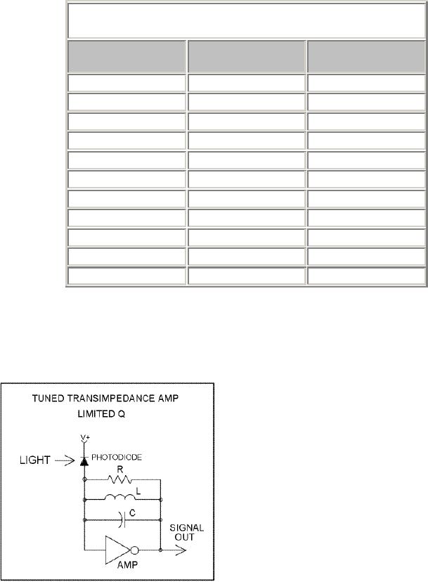
Typical
Inductor
Self
Resonance Frequencies
Reactance
at
Inductance
Frequency
Res.
Frequency
4H
200KHz
500K
Ohms
100mH
200KHz
100K
Ohms
47mH
250KHz
75K
Ohms
27mH
300KHz
50K
Ohms
15mH
500HKz
50K
Ohms
10mH
700KHz
40K
Ohms
4.7mH
800KHz
22K
Ohms
2.2mH
1MHz
14K
Ohms
1mH
2HMz
12K
Ohms
470uH
3MHz
9K
Ohms
100uH
7MHz
4.4K
Ohms
Figure
6f
Transimpedance
Amplifier Detector Circuit
with Limited Q
The
use of a LC tuned circuit in a
transimpedance amplifier circuit does
improve the current
to
voltage
conversion and does reject
much of the
signals
associated with ambient
light. But, high Q
circuits
are prone to unwanted
oscillations. As
shown
in figure
6g, to keep
the circuit from
misbehaving,
a resistor should be wired in
parallel
with
the inductor. The effect of
the resistor is to
lower
the circuit's Q. For pulse
stream applications
with
low duty cycles (short
pulses with lots of
time
between
pulses), it is best to keep
the Q near 1. A Q
of
one exists when the
reactance of the coil is
equal
to
the parallel resistance at
the desired frequency.
If
higher
Qs were used, with low
duty cycle pulse
streams,
the transimpedance amplifier
would
produce
excessive ringing with each
pulse and
would
be prone to self-oscillation.
Figure
6g
Page
47
of 68
Optical
Through-the-Air Communications Handbook
-David A. Johnson, PE
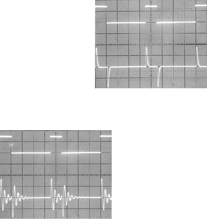
Figure
6h and
6i
illustrate
what happens
in
a circuit with a low Q and
high Q when
processing
single pulses. If higher
duty
cycle
pulse trains are being
transmitted,
higher
Qs can be used. In near 50%
duty
cycle
transmission systems, Qs in excess
of
50 are possible with a careful
design.
Table
6f
lists
the typical
self-resonant
frequency
of some inductors. If you
don't
know
the self-resonant frequency of a
coil
you
can use the schematic shown
in figure
6e
on page 52 to measure
it.
In
low duty cycle light
pulse applications,
the
inductor value should be chosen
based
Figure
6h
on
the width of the light
pulse being sent
by
the transmitter. The
self-resonant period (1/frequency) of
the coil should equal
2W, where W is
the
width of the light pulse.
Since the circuit layout,
the amplifier circuit and
the PIN diode will
all
add
to the overall circuit capacitance,
some experimentation will be necessary to
determine the best
inductor
value for the particular
application. The equation
2pFL should be used to
calculate the
value
of the resistor wired in
parallel to the inductor to
limit the Q to 1.
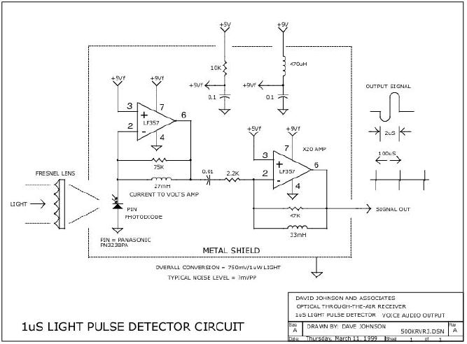
Figure
6j on page 53 is an
example of a
complete
transimpedance amplifier circuit
with
inductive feedback. The
amplifier
circuit
shown in figure
6j on page 53 has
a
light
power to voltage conversion of
about
23
millivolts per milliwatt (assuming
50%
PIN
conversion) when used with
1
microsecond
light pulses. Such
an
amplifier
should be able to detect light
pulses
as weak as one nanowatt
during
dark
nighttime conditions.
Post
Signal Amplifier
As
discussed above, the
transimpedance
amplifier
converts the PIN current to
a
Figure
6i
voltage.
However, it may be too much
to
expect
one amplifier stage to boost the
signal of interest to a useful
level. Typically, one or
more
voltage
amplifier stages after the
front end circuit are
needed. Often the post
amplifiers will include
some
additional signal filters so
only the desired signals
are amplified, rejecting
more of the
undesired
noise. A general purpose post amplifier
is shown in figure
6j on page 53.
The
circuit uses a quality
operational amplifier in conjunction
with some filter circuits
designed to
process
light pulses lasting about 1
micro second. The circuit
boosts the signal by a
factor of X20.
Signal
Pulse Discriminators
Page
48
of 68
Optical
Through-the-Air Communications Handbook
-David A. Johnson, PE
Once
the signal has been
sufficiently amplified and filtered, it
often needs to be
separated
completely
from any background noise.
Since most systems use pulse
frequency modulation
techniques
to transmit the information,
the most common method to
separate the signal from
noise
is
with the use of a voltage
comparator. The comparator can
produce an output signal
that is
thousands
of times higher in amplitude
than the input signal. As an
example, a properly
designed
comparator
circuit can produce a 5 volt
peak to peak TTL logic
output signal from a input
of only a
few
millivolts.
But,
to insure that the
comparator can faithfully extract
the signal of interest, the
signal must be
greater
in amplitude than any noise by a sizeable
margin. For most
applications, I recommend
that
the
signal to noise ratio exceed a
factor of at least 10:1 (20db).
Then, with a properly
designed
comparator
circuit, the comparator
output would change state
(toggle) only when a signal
is present
and
will not be effected by
noise.
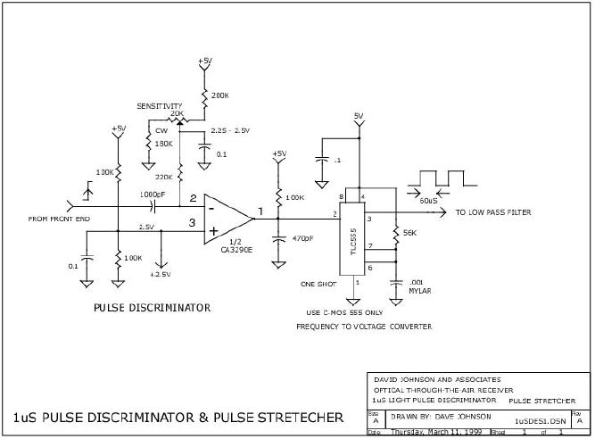
A
complete signal discriminator
circuit is shown in figure
6k on page 54. The
circuit is designed so
a
positive input pulse needs
to exceed a threshold voltage
before the comparator produces
a
negative
output pulse. A variable
resistor network allows the
threshold voltage to be adjustable.
The
adjustment
thereby provides a means to
set the sensitivity of the
circuit. The adjustment
should be
made
under the worst case
bright background conditions so
the noise produced by the
bright
background
light does not toggle
the comparator.
Frequency
to Voltage Converters
If
the light pulses being
transmitted are frequency
modulated to carry the
information, then the
reverse
must be done to restore the original
information. The pulse
frequency must therefore
be
converted
back into the original
amplitude changing signal. A
simple but very effective
frequency
to
voltage converter circuit is
shown in figure
6k on page 54.
Each
pulse from the
pulse
discriminator
circuit is converted into a
well defined logic level
pulse that lasts for a
specific time.
As
the frequency increases and
decreases, the time between
the pulses will change. The
changing
frequency
will therefore cause the
average voltage level of the
signal produced by the
converter to
change
by the same proportion. To
remove the unwanted carrier
frequency from the
desired
modulation
frequency, the output of the
converter must be
filtered.
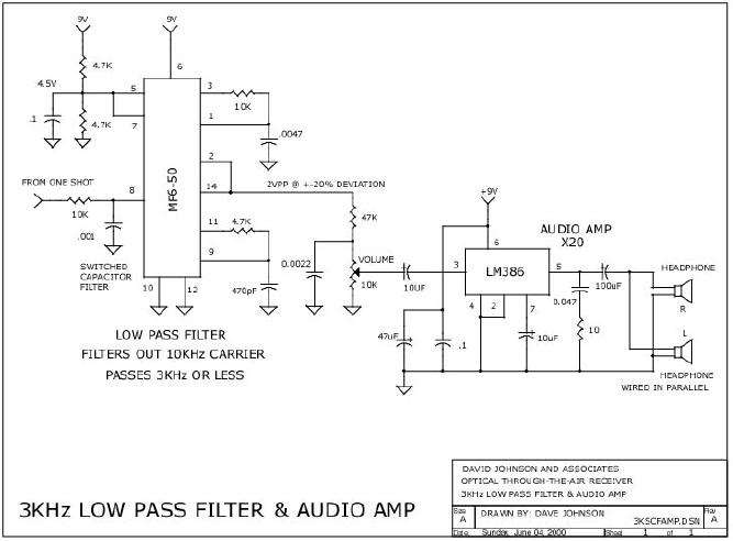
Modulation
Frequency Filters
A
complete filter circuit is
shown in figure
6l on page 55. The
circuit uses a switched
capacitor
filter
(SCF) integrated circuit
from National Semiconductor.
With the values chosen, the
circuit
removes
the majority of a 10KHz
carrier signal, leaving the
wanted voice audio
frequencies. The
filter's
cutoff frequency is set at
about 3KHz that is the
minimum upper frequency
needed for voice
audio.
Audio
Power Amplifiers
The
final circuit needed to
complete a voice grade light
pulse receiver is an audio
power amplifier.
The
circuit shown in figure
6l on page 55 uses a
single inexpensive LM386 IC.
The circuit is
designed
to drive a pair of audio headphones.
The variable resistor shown
is used to adjust the
audio
volume.
Since the voice audio system
described above does not
transmit stereo audio, the
left and
right
headphones are wired in
parallel so both ears
receive the same audio
signal.
Light
Receiver Noise
Considerations
Page
49
of 68
Optical
Through-the-Air Communications Handbook
-David A. Johnson, PE
One
of the most difficult
problems to overcome in an optical
through the air
communications
system
is ambient light. Any stray
sunlight or bright background
light that is collected by
the
receiver
optics and focused onto the
light detector will produce a
large steady state DC
level
through
the detector circuit.
Although much of the DC is
ignored with the use of an
inductive
feedback
amplifier method in the
front-end circuit, the large
DC component in the light
detector
will
produce some unwanted broadband
noise. The noise is very
much like the background
static
you
may hear on an AM radio when
tuning the dial between
stations. As discussed in the
section on
light
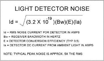
detectors, the amount of noise produced
by the detector is
predictable.
The
equation shown in
figure
6m
describes
how the detector noise
varies
with
ambient light. The
relationship
follows
a square root function. That
means
if
the ambient light level
increases by a
factor
of four, the noise produced at
the
detector
only doubles. This
characteristic
both
helps and hurts a light
receiver
circuit,
depending on whether the
system
is
being used during the
light of day or
during
the dark of night. The
equation
Figure
6m
predicts
that for high ambient
daytime
conditions,
you will have to dramatically reduce
the amount of ambient light
striking the detector
in
order
to see an significant reduction in
the amount of noise produced at
the detector circuit.
The
equation
also describes that under
dark nighttime conditions,
the stray light has to
dramatically
increase
in order to produce a sizable
elevation in noise. If the
system must work during
both day
and
night, it will have to contend
with the worst daytime noise
conditions. Conversely, some
light
receivers
could take advantage of the low
stray light conditions found
at night and produce a
communications
system with a much longer
range than would be otherwise possible if
it were used
during
daylight.
As
mentioned above, inserting an
optical filter between the
lens and the light detector
can reduce
the
effects of ambient light.
But, as shown by the noise
equation, the amount of
light hitting the
detector
needs to be dramatically reduced to
produce a sizable reduction in
the induced noise.
Since
most
sunlight contains a sizable
amount of infrared light,
such filters do not reduce
the noise level
very
much. However, very narrow
band filters that can be selected to
match the wavelength of
a
laser
diode light source, are effective in
reducing ambient light and
therefore noise.
Other
Receiver Circuits
The
circuits described above were
designed for a voice audio
communications system that
received
narrow
1uS light pulses. An experimenter may
wish to use other modulation
frequencies. In
addition,
untuned broad band receiver circuits
are handy when monitoring
modulated light
signals
where
the frequency is not known.
I have included some
additional circuits below
that you may
find
helpful.
A
very simple and inexpensive broad band
light receiver circuit is
shown in figure
6n on page 56.
The
circuit uses a CD4069UB
C-MOS logic integrated
circuit. Make sure to use
the unbuffered UB
version
of this popular device. The
first section of the circuit
performs the current to
voltage
conversion.
The other section provides
voltage gain. The overall
conversion is about 2 volts
per
Page
50
of 68
Optical
Through-the-Air Communications Handbook
-David A. Johnson, PE
microwatt.
With the values shown,
the circuit will work with
light modulation frequencies
between
1KHz
and 200KHz.
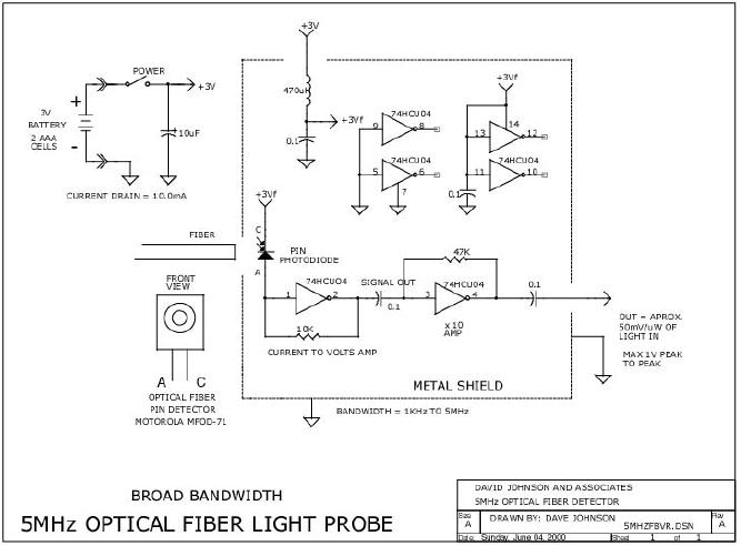
A
similar circuit is shown in
figure
6o on page 57. It uses a
much faster 74HCU04 device
instead
of
the CD4069UB. The circuit
should be operated from a 3v
supply. For real
flexibility, I have
shown
how a Motorola MFOD-71
optical fiber photodiode
module can be used. The
circuit's 2MHz
bandwidth
is great when monitoring light pulses
with fast edges. A section
of inexpensive plastic
optical
fiber can be attached to the detector and
used as a light probe to inspect
the output from
various
modulated light sources. Keep in mind,
that since both broad band circuits do
not use an
inductor
in the feedback circuit, they
should only be operated in
low ambient light
conditions.
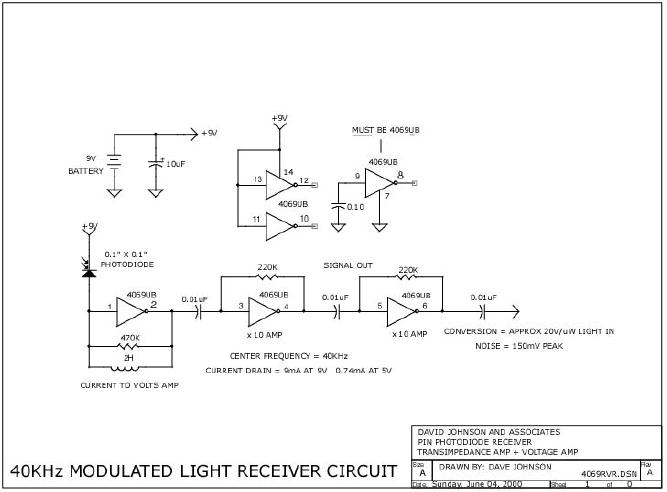
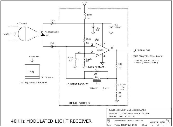
A
very sensitive light
receiver circuit, designed
for detecting the 40KHz
signal used by many
optical
remote control devices, is shown in
figure
6p on page 58. The
circuit shown uses a one
inch
plastic
lens in conjunction with a
large 10mm X 10mm
photodiode. With the values
chosen, the
circuit
will detect light from a typical
optical remote from several
hundred feet away. If the
remote
control
circuit also used a small
lens the separation distance could
extend to several
miles.
Page
51
of 68
Optical
Through-the-Air Communications Handbook
-David A. Johnson, PE
Figure
6e
Page
52
of 68
Optical
Through-the-Air Communications Handbook
-David A. Johnson, PE
Figure
6j
Page
53
of 68
Optical
Through-the-Air Communications Handbook
-David A. Johnson, PE
Figure
6k
Page
54
of 68
Optical
Through-the-Air Communications Handbook
-David A. Johnson, PE
Figure
6l
Page
55
of 68
Optical
Through-the-Air Communications Handbook
-David A. Johnson, PE
Figure
6n
Page
56
of 68
Optical
Through-the-Air Communications Handbook
-David A. Johnson, PE
Figure
6o
Page
57
of 68
Optical
Through-the-Air Communications Handbook
-David A. Johnson, PE
Figure
6p
Page
58
of 68
Optical
Through-the-Air Communications Handbook
-David A. Johnson,
PE
Table of Contents:
- LIGHT THEORY:The Spectrum, Human Eye Response, Silicon Detector Response
- LIGHT DETECTORS:The Silicon PIN Photodiode, Active Area, Response Time
- LIGHT EMITTERS:Light Emitting Diodes (LEDs), Solid State Semiconductor Lasers
- LIGHT SYSTEMS CONFIGURATIONS:Opposed Configuration, Diffuse Reflective Configuration
- LIGHT PROCESSING THEORY:Lenses as Antennas, Light Collimators and Collectors
- OPTICAL RECEIVER CIRCUITS:Current to Voltage Converter Circuits, Post Signal Amplifiers
- OPTICAL TRANSMITTER CIRCUITS:Audio Amplifier with Filters, Pulsed Light Emitters